

Page 1

PCA9536
4-bit I2C-bus and SMBus I/O port
Rev. 6 — 7 November 2017 Product data sheet
1. General description
The PCA9536 is an 8-pin CMOS device that provides 4 bits of General Purpose paralle l
Input/Output (GPIO) expansion for I
enhance the NXP Semiconductors family of I
provide a simple solution when additional I/O is needed for ACPI power switches,
sensors, push buttons, LEDs, fans, etc.
The PCA9536 consists of a 4-bit Configuration register (input or output selection), 4-bit
Input Port register, 4-bit Output Port register and a 4-bit Polarity Inversion register
(active HIGH or active LOW operation). The system master can enable the I/Os as either
inputs or outputs by writing to the I/O configuration bits. The data for each input or output
is kept in the corresponding Input Port or Output Port register. The polarity of the read
register can be inverted with the Polarity Inversion register. All registers can be read by
the system master.
The power-on reset sets the registers to their default values and initializes the device state
machine.
2
C-bus address is fixed and allows only one device on the same I2C-bus/SMBus.
The I
2. Features and benefits
4-bit I2C-bus GPIO
Operating power supply voltage range of 2.3 V to 5.5 V
5 V tolerant I/Os
Polarity Inversion register
Low standby current
Noise filter on SCL/SDA inputs
No glitch on power-up
Internal power-on reset
4 I/O pins which default to 4 inputs with 100 k internal pull-up resistor
0 Hz to 400 kHz clock frequency
ESD protection exceeds 2000 V HBM per JESD22-A114, 200 V MM per
JESD22-A115 and 1000 V CDM per JESD22-C101
Latch-up testing is done to JEDEC Standard JESD78 which exceeds 100 mA
Packages offered: SO8, TSSOP8 (MSOP8), HVSON8
2
C-bus/SMBus applications and was developed to
2
C-bus I/O expanders. I/O expanders
Page 2
NXP Semiconductors
3. Ordering information
PCA9536
4-bit I2C-bus and SMBus I/O port
Table 1. Ordering information
=40C to +85C
T
amb
Type
number
Topside
mark
Package
Name Description Version
PCA9536D PCA9536 SO8 plastic small outline package; 8 leads; body width 3.9 mm SOT96-1
[1]
PCA9536DP 9536 TSSOP8
PCA9536TK 9536 HVSON8 plastic thermal enhanced very thin small outline package; no leads;
plastic thin shrink small outline package; 8 leads; body width 3 m m SOT505-1
SOT908-1
8 terminals; bo dy 3 3 0.85 mm
[1] Also known as MSOP8.
3.1 Ordering options
Table 2. Ordering options
Type number Orderable
PCA9536D PCA9536D,112 SO8 ST ANDARD
PCA9536DP PCA9536DP,118 TSSOP8
PCA9536TK PCA9536TK,118 HVSON8 REEL 13" Q1/T1
Package Packing method Minimum
part number
MARKING * IC'S
TUBE - DSC BULK
PACK
PCA9536D,118 SO8 REEL 13" Q1/T1
*STANDARD MARK
SMD
[1]
REEL 13" Q1/T1
*STANDARD MARK
SMD
*STANDARD MARK
SMD
order quantity
2000 T
2500 T
2500 T
6000 T
Temperature
= 40 C to +85 C
amb
= 40 C to +85 C
amb
= 40 C to +85 C
amb
= 40 C to +85 C
amb
PCA9536 All information provided in this document is subject to legal disclaimers. © NXP Semiconductors N.V. 2017. All rights reserved.
Product data sheet Rev. 6 — 7 November 2017 2 of 24
Page 3
NXP Semiconductors
PCA9536
POWER-ON
RESET
002aab851
I2C-BUS/SMBus
CONTROL
INPUT
FILTER
SCL
SDA
V
DD
INPUT/
OUTPUT
PORTS
IO0
V
SS
4-bit
write pulse
read pulse
IO1
IO2
IO3
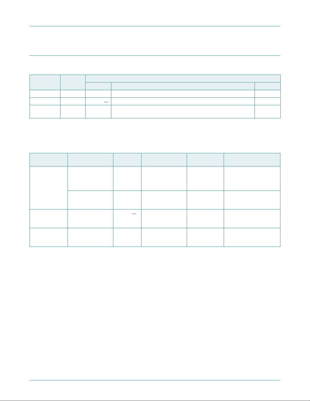
4. Block diagram
Fig 1. Block diagram of PCA9536
PCA9536
4-bit I2C-bus and SMBus I/O port
All I/Os are set to inputs at reset.
PCA9536 All information provided in this document is subject to legal disclaimers. © NXP Semiconductors N.V. 2017. All rights reserved.
Product data sheet Rev. 6 — 7 November 2017 3 of 24
Page 4
NXP Semiconductors
PCA9536D
IO0 V
DD
IO1 SDA
IO2
SCL
V
SS
IO3
002aab849
1
2
3
4
6
5
8
7
PCA9536DP
IO0 V
DD
IO1 SDA
IO2 SCL
V
SS
IO3
002aab850
1
2
3
4
6
5
8
7
002aac459
IO3
SCLIO2
SDAIO1
V
DD
IO0
Transparent top view
54
63
72
81
terminal 1
index area
PCA9536TK
V
SS
5. Pinning information
5.1 Pinning
Fig 2. Pin configuration for SO8 Fig 3. Pin configuration for TSSOP8
PCA9536
4-bit I2C-bus and SMBus I/O port
PCA9536 All information provided in this document is subject to legal disclaimers. © NXP Semiconductors N.V. 2017. All rights reserved.
Product data sheet Rev. 6 — 7 November 2017 4 of 24
Fig 4. Pin configuration for HVSON8
5.2 Pin description
Table 3. Pin description
Symbol Pin Description
IO0 1 input/output 0
IO1 2 input/output 1
IO2 3 input/output 2
V
SS
IO3 5 input/output 3
SCL 6 serial clock line
SDA 7 serial data line
V
DD
4 supply ground
8 supply voltage
Page 5
NXP Semiconductors
6. Functional description
Refer to Figure 1 “Block diagram of PCA9536”.
6.1 Registers
6.1.1 Command byte
Table 4. Command byte
Command Protocol Function
0 read byte Input Port register
1 read/write byte Output Port register
2 read/write byte Polarity Inversion register
3 read/write byte Configuration register
The command byte is the first byte to follow the address byte during a write transmission.
It is used as a pointer to determine which of the following registers will be written or read.
PCA9536
4-bit I2C-bus and SMBus I/O port
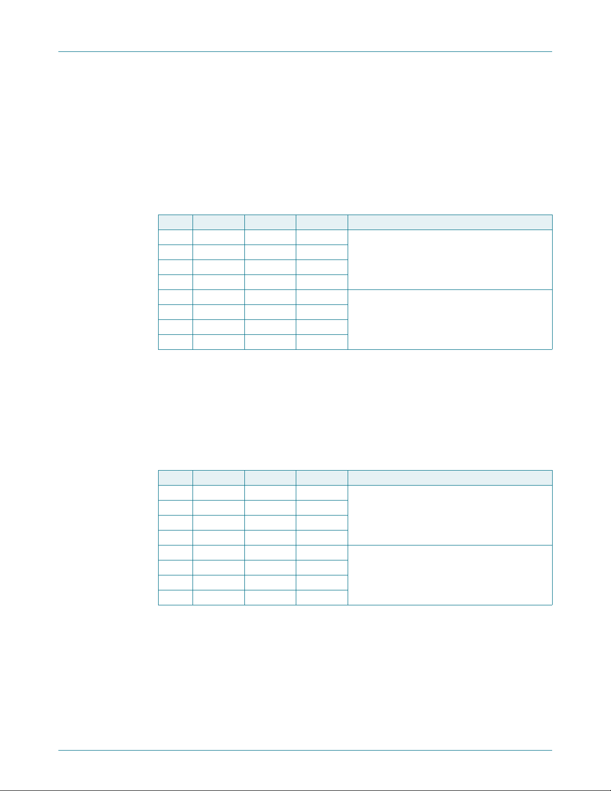
6.1.2 Register 0 - Input Port register
This register is a read-only port. It reflects the incoming logic levels of the pins, regardless
of whether the pin is defined as an input or an output by Register 3. Writes to this register
have no effect.
The default ‘X’ is determined by the externally applied logic level, normally logic 1 when
no external signal externally applied because of the internal pull-up resistors.
Table 5. Register 0 - Input Port register bit description
Legend: * default value
Bit Symbol Access Value Description
7 I7 read only 1* not used
6 I6 read only 1*
5 I5 read only 1*
4 I4 read only 1*
3 I3 read only X determined by external ly applied logic level
2 I2 read only X
1 I1 read only X
0 I0 read only X
PCA9536 All information provided in this document is subject to legal disclaimers. © NXP Semiconductors N.V. 2017. All rights reserved.
Product data sheet Rev. 6 — 7 November 2017 5 of 24
Page 6
NXP Semiconductors
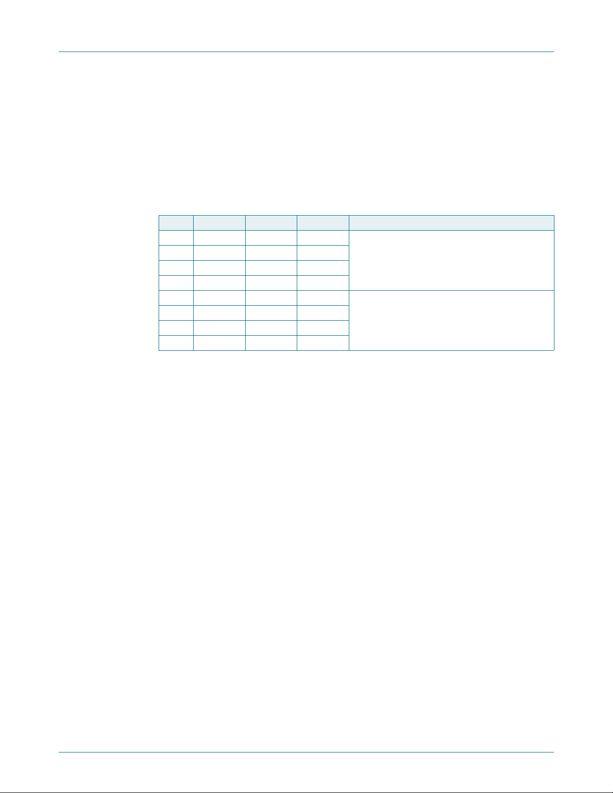
6.1.3 Register 1 - Output Port register
This register reflects the outgoing logic levels of the p ins defined as outpu ts by Register 3.
Bit values in this register have no effect on pins defined as input s. Reads from this register
return the value that is in the flip-flop controlling the output selection, not the actual pin
value.
‘Not used’ bits can be programmed with either logic 0 or logic 1.
Table 6. Register 1 - Output Port register bit description
Legend: * default value
Bit Symbol Access Value Description
7 O7 R 1* not used
6O6 R 1*
5O5 R 1*
4O4 R 1*
3 O3 R 1* reflects outgoing logic levels of pins defined as
2O2 R 1*
1O1 R 1*
0O0 R 1*
PCA9536
4-bit I2C-bus and SMBus I/O port
outputs by Register 3
6.1.4 Register 2 - Polarity Inversion register
This register allows the user to invert the polarity of the Input Port register data. If a bit in
this register is set (written with ‘1’), the corresponding Input Port data is inverted. If a bit in
this register is cleared (written with a ‘0’), the Input Port data polarity is retained.
‘Not used’ bits can be programmed with either logic 0 or logic 1.
Table 7. Register 2 - Polarity Inversion register bit description
Legend: * default value
Bit Symbol Access Value Description
7 N7 R/W 0* not used
6N6 R/W 0*
5N5 R/W 0*
4N4 R/W 0*
3 N3 R/W 0* inverts polarity of Input Port register data
2N2 R/W 0*
1N1 R/W 0*
0N0 R/W 0*
0 = Input Port register data retained (default
value)
1 = Input Port register data inverted
PCA9536 All information provided in this document is subject to legal disclaimers. © NXP Semiconductors N.V. 2017. All rights reserved.
Product data sheet Rev. 6 — 7 November 2017 6 of 24
Page 7
NXP Semiconductors
6.1.5 Register 3 - Configuration register
This register configures the directions of the I/O pins. If a bit in this register is set, the
corresponding port pin is enabled as an input with high-impedance output driver. If a bit in
this register is cleared, the corresponding port pin is enabled as an output. At reset, the
I/Os are configured as inputs with a weak pull-up to V
‘Not used’ bits can be programmed with either logic 0 or logic 1.
Table 8. Register 3 - Configuration register bit description
Legend: * default value
Bit Symbol Access Value Description
7 C7 R/W 1* not used
6C6 R/W 1*
5C5 R/W 1*
4C4 R/W 1*
3 C3 R/W 1* configures the directions of the I/O pins
2C2 R/W 1*
1C1 R/W 1*
0C0 R/W 1*
PCA9536
4-bit I2C-bus and SMBus I/O port
.
DD
0 = corresponding port pin enabled as an output
1 = corresponding port pin configured as input
(default value)
6.2 Power-on reset
When power is applied to VDD, an internal Power-On Reset (POR) holds the PCA9536 in
a reset condition until V
has reached V
DD
. At that point, the reset condition is released
POR
and the PCA9536 registers and state machine will initialize to their default states.
Thereafter, V
For a power reset cycle, V
must be lowered below 0.2 V to reset the device.
DD
must be lowered below 0.2 V and then restored to the
DD
operating voltage.
6.3 I/O port
When an I/O is configured as an input, FETs Q1 and Q2 are off, creating a
high-impedance input with a weak pull-up (100 k typical) to V
be raised above V
to a maximum of 5.5 V.
DD
If the I/O is configured as an output, then either Q1 or Q2 is enabled, depending on the
state of the Output Port register . Ca re should be exercised if an external volt age is app lied
to an I/O configured as an output because of the low-impedance paths that exist between
the pin and either V
or VSS.
DD
. The input voltage may
DD
PCA9536 All information provided in this document is subject to legal disclaimers. © NXP Semiconductors N.V. 2017. All rights reserved.
Product data sheet Rev. 6 — 7 November 2017 7 of 24
Page 8

NXP Semiconductors
V
DD
IO0 to IO3
output port
register data
configuration
register
DQ
CK Q
data from
shift register
write configuration
pulse
output port
register
DQ
CK
write pulse
polarity inversion
register
DQ
CK
data from
shift register
write polarity
pulse
input port
register
DQ
CK
read pulse
input port
register data
polarity inversion
register data
002aab852
FF
data from
shift register
FF
FF
FF
Q1
100 kΩ
Q2
V
SS
R/W
002aab853
1 0 0 0 0 0 1
fixed
slave address
PCA9536
4-bit I2C-bus and SMBus I/O port
Remark: At power-on reset, all registers return to default values.
Fig 5. Simplified schematic of IO0 to IO3
6.4 Device address
Fig 6. PCA9536 device address
6.5 Bus transactions
Data is transmitted to the PCA9536 registers using the Write mode as shown in Figure 7
and Figure 8
Figure 9
once a command byte has been sent, the register which was addressed will continue to
be accessed by reads until a new command byte has been sent.
. Data is read from the PCA953 6 reg isters usin g the Read mode a s shown in
and Figure 10. These devices do not implement an auto-increment function, so
PCA9536 All information provided in this document is subject to legal disclaimers. © NXP Semiconductors N.V. 2017. All rights reserved.
Product data sheet Rev. 6 — 7 November 2017 8 of 24
Page 9

NXP Semiconductors
0000010AS1
START condition R/W
acknowledge
from slave
002aab854
A
acknowledge
from slave
SCL
SDA
A
write to port
data out
from port
P
t
v(Q)
987654321
command byte
acknowledge
from slave
data to port
DATA 1
slave address
00000010
STOP
condition
data 1 valid
0000010AS1
START condition R/W
acknowledge
from slave
002aab855
A
acknowledge
from slave
SCL
SDA
A
data to
register
P
987654321
command byte
acknowledge
from slave
data to register
DATA
slave address
0000001/00
STOP
condition
0000010AS1
START condition R/W
acknowledge
from slave
002aab856
A
acknowledge
from slave
SDA
A P
command byte
acknowledge
from master
data from register
DATA (first byte)
slave address
STOP
condition
S
(repeated)
START condition
(cont.)
(cont.)
0000011A1
R/W
acknowledge
from slave
slave address
at this moment master-transmitter becomes master-receiver
and slave-receiver becomes slave-transmitter
NA
no acknowledge
from master
data from register
DATA (last byte)
Fig 7. Write to Output Port reg is ter
PCA9536
4-bit I2C-bus and SMBus I/O port
Fig 8. Write to Configuration register or Polarity Inversion register
Fig 9. Read from register
PCA9536 All information provided in this document is subject to legal disclaimers. © NXP Semiconductors N.V. 2017. All rights reserved.
Product data sheet Rev. 6 — 7 November 2017 9 of 24
Page 10

NXP Semiconductors
0000011AS1
START condition R/W
acknowledge
from slave
002aab857
A
acknowledge
from master
SCL
SDA
NA
read from
port
data into
port
P
t
h(D)
987654321
data from port
no acknowledge
from master
data from port
DATA 4
slave address
DATA 1
STOP
condition
DATA 2 DATA 3 DATA 4
t
su(D)
PCA9536
IO0
IO1
SDA
SCL
V
DD
002aab858
SDA
SCL
10 kΩ 10 kΩ
IO2
IO3
V
DD
V
SS
MASTER
CONTROLLER
V
SS
V
DD
2 kΩ
SUBSYSTEM 1
(e.g. temp. sensor)
INT
SUBSYSTEM 2
(e.g. counter)
RESET
controlled switch
(e.g. CBT device)
A
B
enable
This figure assumes the command byte has previously been programmed with 00h.
Transfer of data can be stopped at any moment by a STOP condition.
Fig 10. Read Input Port register
PCA9536
4-bit I2C-bus and SMBus I/O port
7. Application design-in information
PCA9536 All information provided in this document is subject to legal disclaimers. © NXP Semiconductors N.V. 2017. All rights reserved.
Product data sheet Rev. 6 — 7 November 2017 10 of 24
Device address is 1000 001X; IO0, IO2, IO3 configured as outputs; IO1 configured as input.
Fig 11. Typical application
Page 11

NXP Semiconductors
8. Limiting values
Table 9. Limiting values
In accordance with the Absolute Maximum Rating System (IEC 60134).
Symbol Parameter Conditions Min Max Unit
V
DD
I
I
V
I/O
I
O(IOn)
I
DD
I
SS
P
tot
T
stg
T
amb
T
j(max)
PCA9536
4-bit I2C-bus and SMBus I/O port
supply voltage 0.5 +6.0 V
input current - 20 mA
voltage on an input/output pin VSS 0.5 5.5 V
output current on pin IOn - 50 mA
supply current - 85 mA
ground supply current - 100 mA
total power dissipation - 200 mW
storage temperature 65 +150 C
ambient temperature 40 +85 C
maximum junction temperature - +125 C
PCA9536 All information provided in this document is subject to legal disclaimers. © NXP Semiconductors N.V. 2017. All rights reserved.
Product data sheet Rev. 6 — 7 November 2017 11 of 24
Page 12

NXP Semiconductors
9. Static characteristics
PCA9536
4-bit I2C-bus and SMBus I/O port
Table 10. Static characteristics
= 2.3 V to 5.5 V; VSS=0V; T
V
DD
=40C to +85C; unless otherwise specified.
amb
Symbol Parameter Conditions Min Typ Max Unit
Supplies
V
I
I
V
DD
DD
stb
POR
supply voltage 2.3 - 5.5 V
supply current operating mode; VDD=5.5V;
no load ; f
= 100 kHz
SCL
standby current Standby mode; VDD= 5.5 V; no load;
; f
V
I=VSS
Standby mode; V
VI=VDD; f
= 0 kHz; I/O = inputs
SCL
= 5.5 V; no load;
DD
= 0 kHz; I/O = inputs
SCL
power-on reset voltage
- 290 400 A
- 225 350 A
-0.251 A
[1]
-1.72.2V
Input SCL; input/output SDA
V
IL
V
IH
I
OL
I
L
C
i
LOW-level input voltage 0.5 - +0.3V
HIGH-level input voltage 0.7V
-5.5V
DD
LOW-level output current VOL=0.4V 3 6 - mA
leakage current VI=VDD=V
input capacitance VI=V
SS
SS
1- +1 A
- 6 10 pF
DD
V
I/Os
V
V
I
V
I
IL
IH
OL
OH
LIH
LOW-level input voltage 0.5 - +0.8 V
HIGH-level input voltage 2.0 - 5.5 V
LOW-level output current VOL=0.5V; VDD=2.3V
=0.7V; VDD=2.3V
V
OL
=0.5V; VDD=3.0V
V
OL
=0.7V; VDD=3.0V
V
OL
=0.5V; VDD=4.5V
V
OL
=0.7V; VDD=4.5V
V
OL
HIGH-level output voltage IOH= 8mA; VDD=2.3V
= 10 mA; VDD=2.3V
I
OH
= 8mA; VDD=3.0V
I
OH
= 10 mA; VDD=3.0V
I
OH
= 8mA; VDD=4.75V
I
OH
= 10 mA; VDD=4.75V
I
OH
HIGH-level input leakage
VDD=3.6V; VI=V
DD
[2]
810- mA
[2]
10 13 - mA
[2]
814- mA
[2]
10 19 - mA
[2]
817- mA
[2]
10 24 - mA
[3]
1.8 - - V
[3]
1.7 - - V
[3]
2.6 - - V
[3]
2.5 - - V
[3]
4.1 - - V
[3]
4.0 - - V
--1 A
current
I
LIL
LOW-level input leakage
VDD=5.5V; VI=V
SS
--100 A
current
C
i
C
o
input capacitance - 3.7 5 pF
output capacitance - 3.7 5 pF
[1] VDD must be lowered to 0.2 V in order to reset part.
[2] Each I/O must be externally limited to a maximum of 25 mA and the device must be limited to a maximum current of 100 mA.
[3] The total current sourced by all I/Os must be limited to 85 mA.
PCA9536 All information provided in this document is subject to legal disclaimers. © NXP Semiconductors N.V. 2017. All rights reserved.
Product data sheet Rev. 6 — 7 November 2017 12 of 24
Page 13

NXP Semiconductors
10. Dynamic characteristics
PCA9536
4-bit I2C-bus and SMBus I/O port
Table 11. Dynamic characteristics
Symbol Parameter Conditions Standard-mode
2
C-bus
I
Min Max Min Max
f
SCL
t
BUF
SCL clock frequency 0 100 0 400 kHz
bus free time between a STOP and
4.7 - 1.3 - s
START condition
t
HD;STA
t
SU;STA
hold time (repeated) START condition 4.0 - 0.6 - s
set-up time for a repeated START
4.7 - 0.6 - s
condition
t
SU;STO
t
HD;DAT
t
VD;ACK
t
VD;DAT
t
SU;DAT
t
LOW
t
HIGH
t
r
t
f
t
SP
set-up time for STOP condition 4.0 - 0.6 - s
data hold time 0 - 0 - s
data valid acknowledge time
data valid time
[1]
0.3 3.45 0.1 0.9 s
[2]
300 - 50 - ns
data set-up time 250 - 100 - ns
LOW period of the SCL clock 4.7 - 1.3 - s
HIGH period of the SCL clock 4.0 - 0.6 - s
rise time of both SDA and SCL signals - 1000 20 + 0.1C
fall time of both SDA and SCL signals - 300 20 + 0.1C
pulse width of spikes that must be
- 50 - 50 ns
suppressed by the input filter
Port timing
t
v(Q)
t
su(D)
t
h(D)
data output valid time - 200 - 200 ns
data input set-up time 100 - 100 - ns
data input hold time 1 - 1 - s
Fast-mode I2C-bus Unit
[3]
300 ns
b
[3]
300 ns
b
[1] t
[2] t
[3] C
SDA
SCL
= time for Acknowledgement signal from SCL LOW to SDA (out) LOW.
VD;ACK
= minimum time for SDA data output to be valid following SCL LOW.
VD;DAT
= total capacitance of one bus line in pF.
b
t
BUF
t
LOW
t
HD;STA
t
r
t
HD;DAT
t
HIGH
t
f
t
SU;DAT
0.7 × V
DD
0.3 × V
DD
t
HD;STA
t
SU;STA
Sr
t
SP
t
SU;STO
0.7 × V
DD
0.3 × V
DD
PP S
002aaa986
Fig 12. Definition of timing
PCA9536 All information provided in this document is subject to legal disclaimers. © NXP Semiconductors N.V. 2017. All rights reserved.
Product data sheet Rev. 6 — 7 November 2017 13 of 24
Page 14

NXP Semiconductors
002aab175
protocol
START
condition
(S)
bit 7
MSB
(A7)
bit 6
(A6)
bit 0
(R/W)
acknowledge
(A)
STOP
condition
(P)
SCL
SDA
t
HD;STA
t
SU;DAT
t
HD;DAT
t
f
t
BUF
t
SU;STA
t
LOWtHIGH
t
VD;ACK
t
SU;STO
1 / f
SCL
t
r
t
VD;DAT
0.3 × V
DD
0.7 × V
DD
0.3 × V
DD
0.7 × V
DD
PULSE
GENERATOR
V
O
C
L
50 pF
R
L
500 Ω
002aab880
R
T
V
I
V
DD
DUT
V
DD
open
V
SS
C
L
50 pF
500 Ω
002aab881
2V
DD
open
V
SS
S1
from output
under test
500 Ω
PCA9536
4-bit I2C-bus and SMBus I/O port
Fig 13. I2C-bus timing diagram
11. Test information
Fig 14. Test circuitry for switching times
Rise and fall times refer to VIL and V
IH
RL = load resistor.
C
= load capacitance includes jig and probe capacitance.
L
= termination resistance should be equal to the output impedance Zo of the pulse generators.
R
T
Fig 15. Test circuit
PCA9536 All information provided in this document is subject to legal disclaimers. © NXP Semiconductors N.V. 2017. All rights reserved.
Product data sheet Rev. 6 — 7 November 2017 14 of 24
Table 12. Test data
Test Load Switch
t
v(Q)
C
L
R
L
50 pF 500 2V
DD
Page 15

NXP Semiconductors
UNIT
A
max.
A1A2A3b
p
cD
(1)E(2)
(1)
eHELLpQZywv θ
REFERENCES
OUTLINE
VERSION
EUROPEAN
PROJECTION
ISSUE DATE
IEC JEDEC JEITA
mm
inches
1.75
0.25
0.10
1.45
1.25
0.25
0.49
0.36
0.25
0.19
5.0
4.8
4.0
3.8
1.27
6.2
5.8
1.05
0.7
0.6
0.7
0.3
8
0
o
o
0.25 0.10.25
DIMENSIONS (inch dimensions are derived from the original mm dimensions)
Notes
1. Plastic or metal protrusions of 0.15 mm (0.006 inch) maximum per side are not included.
2. Plastic or metal protrusions of 0.25 mm (0.01 inch) maximum per side are not included.
1.0
0.4
SOT96-1
X
w M
θ
A
A
1
A
2
b
p
D
H
E
L
p
Q
detail X
E
Z
e
c
L
v M
A
(A )
3
A
4
5
pin 1 index
1
8
y
076E03 MS-012
0.069
0.010
0.004
0.057
0.049
0.01
0.019
0.014
0.0100
0.0075
0.20
0.19
0.16
0.15
0.05
0.244
0.228
0.028
0.024
0.028
0.012
0.010.010.041 0.004
0.039
0.016
0 2.5 5 mm
scale
SO8: plastic small outline package; 8 leads; body width 3.9 mm
SOT96-1
99-12-27
03-02-18
12. Package outline
PCA9536
4-bit I2C-bus and SMBus I/O port
Fig 16. Package outline SOT96-1 (SO8)
PCA9536 All information provided in this document is subject to legal disclaimers. © NXP Semiconductors N.V. 2017. All rights reserved.
Product data sheet Rev. 6 — 7 November 2017 15 of 24
Page 16

NXP Semiconductors
UNIT
A
1
A
max.
A2A3b
p
LH
E
L
p
wyv
ceD
(1)E(2)
Z
(1)
θ
REFERENCES
OUTLINE
VERSION
EUROPEAN
PROJECTION
ISSUE DATE
IEC JEDEC JEITA
mm
0.15
0.05
0.95
0.80
0.45
0.25
0.28
0.15
3.1
2.9
3.1
2.9
0.65
5.1
4.7
0.70
0.35
6°
0°
0.1 0.10.10.94
DIMENSIONS (mm are the original dimensions)
Notes
1. Plastic or metal protrusions of 0.15 mm maximum per side are not included.
2. Plastic or metal protrusions of 0.25 mm maximum per side are not included.
0.7
0.4
SOT505-1
99-04-09
03-02-18
w M
b
p
D
Z
e
0.25
14
8
5
θ
A
A
2
A
1
L
p
(A3)
detail X
L
H
E
E
c
v M
A
X
A
y
2.5 5 mm0
scale
TSSOP8: plastic thin shrink small outline package; 8 leads; body width 3 mm
SOT505-1
1.1
pin 1 index
PCA9536
4-bit I2C-bus and SMBus I/O port
Fig 17. Package outline SOT505-1 (TSSOP8)
PCA9536 All information provided in this document is subject to legal disclaimers. © NXP Semiconductors N.V. 2017. All rights reserved.
Product data sheet Rev. 6 — 7 November 2017 16 of 24
Page 17

NXP Semiconductors
0.50.21
0.05
0.00
A
1
E
h
b
UNIT
D
(1)
ye
1.5
e
1
REFERENCES
OUTLINE
VERSION
EUROPEAN
PROJECTION
ISSUE DATE
IEC JEDEC JEITA
mm
3.1
2.9
cD
h
1.65
1.35
y
1
3.1
2.9
2.25
1.95
0.3
0.2
0.05 0.1
DIMENSIONS (mm are the original dimensions)
SOT908-1 MO-229
E
(1)
0.5
0.3
L
0.1v0.05
w
SOT908-1
HVSON8: plastic thermal enhanced very thin small outline package; no leads;
8 terminals; body 3 x 3 x 0.85 mm
A
(1)
max.
05-09-26
05-10-05
Note
1. Plastic or metal protrusions of 0.075 mm maximum per side are not included.
X
terminal 1
index area
B A
D
E
detail X
A
A
1
c
C
y
C
y
1
exposed tie bar (4×)
exposed tie bar (4×)
b
terminal 1
index area
e
1
e
AC
B
v
M
C w
M
E
h
D
h
L
14
58
0 1 2 mm
scale
PCA9536
4-bit I2C-bus and SMBus I/O port
Fig 18. Package outline SOT908-1 (HVSON8)
PCA9536 All information provided in this document is subject to legal disclaimers. © NXP Semiconductors N.V. 2017. All rights reserved.
Product data sheet Rev. 6 — 7 November 2017 17 of 24
Page 18

NXP Semiconductors
13. Handling information
All input and output pins are protected against ElectroStatic Discharge (ESD) under
normal handling. When handling ensure that the appropriate precautions are taken as
described in JESD625-A or equivalent standards.
14. Soldering of SMD packages
This text provides a very brief insight into a complex technology. A more in-depth account
of soldering ICs can be found in Application Note AN10365 “Surface mount reflow
soldering description”.
14.1 Introduction to soldering
Soldering is one of the most common methods through which packages are attached to
Printed Circuit Boards (PCBs), to form electrical circuits. The soldered joint provides both
the mechanical and the electrical connection. There is no single soldering method that is
ideal for all IC packages. Wave soldering is often preferred when through-hole and
Surface Mount Devices (SMDs) are mixed on one printed wiring board; however, it is not
suitable for fine pitch SMDs. Reflow soldering is ideal for the small pitches and high
densities that come with increased miniaturization.
PCA9536
4-bit I2C-bus and SMBus I/O port
14.2 Wave and reflow soldering
Wave soldering is a joining technology in which the joints are made by so lder coming from
a standing wave of liquid solder. The wave soldering process is suitable for the following:
• Through-hole components
• Leaded or leadless SMDs, which are glued to the surface of the printed circuit board
Not all SMDs can be wave soldered. Packages with solder balls, and some leadless
packages which have solder lands underneath the body, cannot be wave soldered. Also,
leaded SMDs with leads having a pitch smaller than ~0.6 mm cannot be wave soldered,
due to an increased probability of bridging.
The reflow soldering process involves applying solder paste to a board, followed by
component placement and exposure to a temperature profile. Leade d packages,
packages with solder balls, and leadless packages are all reflow solderable.
Key characteristics in both wave and reflow soldering are:
• Board specifications, including the board finish, solder masks and vias
• Package footprints, including solder thieves and orientation
• The moisture sensitivity level of the packages
• Package placement
• Inspection and repair
• Lead-free soldering versus SnPb soldering
14.3 Wave soldering
Key characteristics in wave soldering are:
PCA9536 All information provided in this document is subject to legal disclaimers. © NXP Semiconductors N.V. 2017. All rights reserved.
Product data sheet Rev. 6 — 7 November 2017 18 of 24
Page 19

NXP Semiconductors
• Process issues, such as application of adhesive and flux, clinching of leads, board
• Solder bath specifications, including temperature and impurities
14.4 Reflow soldering
Key characteristics in reflow soldering are:
• L ead-free versus SnPb sold ering; note that a lea d-free reflow process usually leads to
• Solder paste printing issues including smearing, release, and adjusting the process
• Reflow temperature profile; this profile includes preheat, reflow (in which the board is
Table 13. SnPb eutectic process (from J-STD-020D)
Package thickness (mm) Package reflow temperature (C)
< 2.5 235 220
2.5 220 220
PCA9536
4-bit I2C-bus and SMBus I/O port
transport, the solder wave parameters, and the time during which components are
exposed to the wave
higher minimum peak temperatures (see Figure 19
reducing the process window
window for a mix of large and small components on one board
heated to the peak temperature) and cooling down. It is imperative that the peak
temperature is high enough for the solder to make reliable solder joint s (a solder paste
characteristic). In addition, the peak temperature must be low enough that the
packages and/or boards are not damaged. The peak temperature of the package
depends on package thickness and volume and is classified in accordance with
Table 13
and 14
Volume (mm3)
< 350 350
) than a SnPb process, thus
Table 14. Lead-free process (from J-STD-020D)
Package thickness (mm) Package reflow temperature (C)
Volume (mm3)
< 350 350 to 2000 > 2000
< 1.6 260 260 260
1.6 to 2.5 260 250 245
> 2.5 250 245 245
Moisture sensitivity precautions, as indicated on the packing, must be respected at all
times.
Studies have shown that small packages reach higher temperatures during reflow
soldering, see Figure 19
PCA9536 All information provided in this document is subject to legal disclaimers. © NXP Semiconductors N.V. 2017. All rights reserved.
Product data sheet Rev. 6 — 7 November 2017 19 of 24
.
Page 20

NXP Semiconductors
001aac844
temperature
time
minimum peak temperature
= minimum soldering temperature
maximum peak temperature
= MSL limit, damage level
peak
temperature
Fig 19. Temperature profiles for large and small components
PCA9536
4-bit I2C-bus and SMBus I/O port
MSL: Moisture Sensitivity Level
For further information on temperature profiles, refer to Application Note AN10365
“Surface mount reflow soldering description”.
15. Abbreviations
Table 15. Abbreviations
Acronym Description
ACPI Advanced Configuration and Power Interface
CDM Charged Device Model
DUT Device Under Test
ESD ElectroStatic Discharge
FET Field-Effect Transistor
GPIO General Purpose Input/Output
HBM Human Body Model
2
C-bus Inter-Integrated Circuit bus
I
I/O Input/Output
LED Light-Emitting Diode
MM Machine Model
POR Power-On Reset
SMBus System Management Bus
PCA9536 All information provided in this document is subject to legal disclaimers. © NXP Semiconductors N.V. 2017. All rights reserved.
Product data sheet Rev. 6 — 7 November 2017 20 of 24
Page 21

NXP Semiconductors
PCA9536
4-bit I2C-bus and SMBus I/O port
16. Revision history
Table 16. Revision history
Document ID Release date Data sheet status Change notice Supersedes
PCA9536 v.6 20171107 Product data sheet 201710002I PCA9536_5
Modifications: • Table 10 “Static characteristics”: Corrected V
• Added Section 3.1 “Ordering options”
PCA9536_5 20100125 Product data sheet - PCA9536_4
Modifications:
• Table 10 “Static characteristics”, sub-section “Supplies”:
– I
Typical value changed from “104 A” to “290 A”
DD
– IDD Maximum value changed from “175 A” to “400 A”
• Table 11 “Dynamic characteristics”: Unit for “t
changed from “s” to “ns”
Remark: The changes made in this revision are to correct typographical errors only. There is
no change in the performance of the device.
PCA9536_4 20070911 Product data sheet - PCA9536_3
PCA9536_3 20061009 Product data sheet - PCA9536_2
PCA9536_2
(9397 750 14124)
PCA9536_1
(9397 750 12895)
20040930 Objective data sheet - PCA9536_1
20040820 Objective data sheet - -
typ and max limit
POR
, fall time of both SDA and SCL signals”
f
PCA9536 All information provided in this document is subject to legal disclaimers. © NXP Semiconductors N.V. 2017. All rights reserved.
Product data sheet Rev. 6 — 7 November 2017 21 of 24
Page 22

NXP Semiconductors
PCA9536
4-bit I2C-bus and SMBus I/O port
17. Legal information
17.1 Data sheet status
Document status
Objective [short] data sheet Development This document contains data from the objective specification for product development.
Preliminary [short] data sheet Qualification This document contains data from the preliminary specification.
Product [short] data sheet Production This document contains the product specification.
[1] Please consult the most recently issued document before initiating or completing a design.
[2] The term ‘short data sheet’ is explained in section “Definitions”.
[3] The product status of device(s) d escribed i n this docume nt may have changed since this docume nt was publis hed and ma y dif fer in case of multiple devices. The latest product statu s
information is available on the Internet at URL http://www.nxp.com.
[1][2]
Product status
[3]
Definition
17.2 Definitions
Draft — The document is a draft version only. The content is still under
internal review and subject to formal approval, which may result in
modifications or additions. NXP Semiconductors does not give any
representations or warranties as to the accuracy or completeness of
information included herein and shall have no liability for the consequences of
use of such information.
Short data sheet — A short data sheet is an extract from a full data sheet
with the same product type number(s) and title. A short data sheet is intended
for quick reference only and should not be relied u pon to cont ain det ailed and
full information. For detailed and full information see the relevant full data
sheet, which is available on request via the local NXP Semiconductors sales
office. In case of any inconsistency or conflict with the short data sheet, the
full data sheet shall prevail.
Product specification — The information and data provided in a Product
data sheet shall define the specification of the product as agreed between
NXP Semiconductors and its customer, unless NXP Semiconductors and
customer have explicitly agreed otherwise in writing. In no event however,
shall an agreement be valid in which the NXP Semiconductors product is
deemed to offer functions and qualities beyond those described in the
Product data sheet.
17.3 Disclaimers
Limited warranty and liability — Information in this document is believed to
be accurate and reliable. However, NXP Semiconductors does not give any
representations or warranties, expressed or implied, as to the accuracy or
completeness of such information and shall have no liability for the
consequences of use of such information. NXP Semiconductors takes no
responsibility for the content in this document if provided by an information
source outside of NXP Semiconductors.
In no event shall NXP Semiconductors be liable for any indirect, incidental,
punitive, special or consequential damages (including - without limitation - lost
profits, lost savings, business interruption, costs related to the removal or
replacement of any products or rework charges) whether or not such
damages are based on tort (including negligence), warranty, breach of
contract or any other legal theory.
Notwithstanding any damages that customer might incur for any reason
whatsoever, NXP Semi conductors’ aggregat e and cumulative liabil ity towards
customer for the products described herein shall be limited in accordance
with the Terms and conditions of commercial sale of NXP Semiconductors.
Right to make changes — NXP Semiconductors reserves the right to make
changes to information published in this document, including without
limitation specifications and product descriptions, at any time and without
notice. This document supersedes and replaces all information supplied prior
to the publication hereof.
PCA9536 All information provided in this document is subject to legal disclaimers. © NXP Semiconductors N.V. 2017. All rights reserved.
Suitability for use — NXP Semiconductors products are not designed,
authorized or warranted to be suitable for use in life support, life-critical or
safety-critical systems or equipment, nor in applications where failure or
malfunction of an NXP Semiconductors product can reasonabl y be expected
to result in personal injury, death or severe property or environmental
damage. NXP Semiconductors and its suppliers accept no liability for
inclusion and/or use of NXP Semiconductors products in such equipment or
applications and therefore such inclusion and/or use is at the cu stomer’s own
risk.
Applications — Applications that are described herein for any of these
products are for illustrative purposes only. NXP Semiconductors makes no
representation or warranty that such applications will be suitable for the
specified use without further testing or modification.
Customers are responsible for the design and operation of their applications
and products using NXP Semiconductors products, and NXP Semiconductors
accepts no liability for any assistance with applications or customer product
design. It is customer’s sole responsibility to determine whether the NXP
Semiconductors product is suitable and fit for the customer’s applications and
products planned, as well as for the planned application and use of
customer’s third party customer(s). Customers should provide appropriate
design and operating safeguards to minimize the risks associated with their
applications and products.
NXP Semiconductors does not accept any liability related to any default ,
damage, costs or problem which is based on any weakness or default in the
customer’s applications or products, or the application or use by customer’s
third party customer(s). Customer is responsible for doing all necessary
testing for the customer’s applications and products using NXP
Semiconductors products in order to avoid a default of the applications and
the products or of the application or use by customer’s third part y
customer(s). NXP does not accept any liability in this respect.
Limiting values — Stress above one or more limiting values (as defined in
the Absolute Maximum Ratings System of IEC 60134) will cause permanent
damage to the device. Limiting values are stress ratings only and (proper)
operation of the device at these or any other conditions above those given in
the Recommended operating conditions section (if present) or the
Characteristics sections of this document is not warranted. Constant or
repeated exposure to limiting values will permanently and irreversibly affect
the quality and reliability of the device.
Terms and conditions of commercial sale — NXP Semiconductors
products are sold subject to the general terms and conditions of commercial
sale, as published at http://www.nxp.com/profile/terms
agreed in a valid written individual agreement. In case an individual
agreement is concluded only the terms and conditions of the respective
agreement shall apply. NXP Semiconductors hereby expressly objects to
applying the customer’s general terms and conditions with regard to the
purchase of NXP Semiconductors products by customer.
No offer to sell or license — Nothing in this document may be interpreted or
construed as an offer to sell product s that is ope n for accept ance or the gr ant,
conveyance or implication of any license under any copyrights, patents or
other industrial or intellectual property rights.
, unless otherwise
Product data sheet Rev. 6 — 7 November 2017 22 of 24
Page 23

NXP Semiconductors
PCA9536
4-bit I2C-bus and SMBus I/O port
Export control — This document as well as the item(s) described herein
may be subject to export control regulations. Export might require a prior
authorization from competent authorities.
Quick reference data — The Quick reference data is an extract of the
product data given in the Limiting values and Characteristics sections of this
document, and as such is not complete, exhaustive or legally binding.
Non-automotive qualified products — Unless this data sheet expressly
states that this specific NXP Semiconductors product is automotive qualified,
the product is not suitable for automotive use. It i s neither qua lif ied nor test ed
in accordance with automotive testing or application requirements. NXP
Semiconductors accepts no liability for inclusion and/or use of
non-automotive qualified products in automotive equ ipment or applications.
In the event that customer uses the product for design-in and use in
automotive applications to automotive specifications and standards, customer
(a) shall use the product without NXP Semiconductors’ warranty of the
product for such automotive applications, use and specifications, and (b)
whenever customer uses the product for automotive applications beyond
NXP Semiconductors’ specifications such use shall be solely at customer’s
own risk, and (c) customer fully indemnifies NXP Semiconductors for any
liability, da mages or failed produ ct cl aims resulting from custome r design and
use of the product for automotive applications beyond NXP Semiconductors’
standard warranty and NXP Semiconductors’ product specifications.
Translations — A non-English (t ranslated) version of a document is for
reference only. The English version shall prevail in case of any discrepancy
between the translated and English versions.
17.4 Trademarks
Notice: All referenced brands, prod uct names, service names and trad emarks
are the property of their respective owners.
2
I
C-bus — logo is a trademark of NXP Semiconductors N.V.
18. Contact information
For more information, please visit: http://www.nxp.com
For sales office addresses, please send an email to: salesaddresses@nxp.com
PCA9536 All information provided in this document is subject to legal disclaimers. © NXP Semiconductors N.V. 2017. All rights reserved.
Product data sheet Rev. 6 — 7 November 2017 23 of 24
Page 24

NXP Semiconductors
19. Contents
1 General description. . . . . . . . . . . . . . . . . . . . . . 1
2 Features and benefits . . . . . . . . . . . . . . . . . . . . 1
3 Ordering information. . . . . . . . . . . . . . . . . . . . . 2
3.1 Ordering options. . . . . . . . . . . . . . . . . . . . . . . . 2
4 Block diagram . . . . . . . . . . . . . . . . . . . . . . . . . . 3
5 Pinning information. . . . . . . . . . . . . . . . . . . . . . 4
5.1 Pinning . . . . . . . . . . . . . . . . . . . . . . . . . . . . . . . 4
5.2 Pin description . . . . . . . . . . . . . . . . . . . . . . . . . 4
6 Functional description . . . . . . . . . . . . . . . . . . . 5
6.1 Registers . . . . . . . . . . . . . . . . . . . . . . . . . . . . . 5
6.1.1 Command byte. . . . . . . . . . . . . . . . . . . . . . . . . 5
6.1.2 Register 0 - Input Port register . . . . . . . . . . . . . 5
6.1.3 Register 1 - Output Port register. . . . . . . . . . . . 6
6.1.4 Register 2 - Polarity Inversion register . . . . . . . 6
6.1.5 Register 3 - Configuration register . . . . . . . . . . 7
6.2 Power-on reset . . . . . . . . . . . . . . . . . . . . . . . . . 7
6.3 I/O port . . . . . . . . . . . . . . . . . . . . . . . . . . . . . . . 7
6.4 Device address. . . . . . . . . . . . . . . . . . . . . . . . . 8
6.5 Bus transactions. . . . . . . . . . . . . . . . . . . . . . . . 8
7 Application design-in information . . . . . . . . . 10
8 Limiting values. . . . . . . . . . . . . . . . . . . . . . . . . 11
9 Static characteristics. . . . . . . . . . . . . . . . . . . . 12
10 Dynamic characteristics . . . . . . . . . . . . . . . . . 13
11 Test information. . . . . . . . . . . . . . . . . . . . . . . . 14
12 Package outline . . . . . . . . . . . . . . . . . . . . . . . . 15
13 Handling information. . . . . . . . . . . . . . . . . . . . 18
14 Soldering of SMD packages . . . . . . . . . . . . . . 18
14.1 Introduction to soldering . . . . . . . . . . . . . . . . . 18
14.2 Wave and reflow soldering . . . . . . . . . . . . . . . 18
14.3 Wave soldering. . . . . . . . . . . . . . . . . . . . . . . . 18
14.4 Reflow soldering. . . . . . . . . . . . . . . . . . . . . . . 19
15 Abbreviations. . . . . . . . . . . . . . . . . . . . . . . . . . 20
16 Revision history. . . . . . . . . . . . . . . . . . . . . . . . 21
17 Legal information. . . . . . . . . . . . . . . . . . . . . . . 22
17.1 Data sheet status . . . . . . . . . . . . . . . . . . . . . . 22
17.2 Definitions. . . . . . . . . . . . . . . . . . . . . . . . . . . . 22
17.3 Disclaimers. . . . . . . . . . . . . . . . . . . . . . . . . . . 22
17.4 Trademarks. . . . . . . . . . . . . . . . . . . . . . . . . . . 23
18 Contact information. . . . . . . . . . . . . . . . . . . . . 23
19 Contents . . . . . . . . . . . . . . . . . . . . . . . . . . . . . . 24
PCA9536
4-bit I2C-bus and SMBus I/O port
Please be aware that important notices concerning this do cument and the product(s)
described herein, have been included in section ‘Legal information’.
© NXP Semiconductors N.V. 2017. All rights reserved.
For more information, please visit: http://www.nxp.com
For sales office addresses, please send an email to: salesaddresses@nxp.com
Date of release: 7 November 2017
Document identifier: PCA9536
 Loading...