

Page 1

PCA9533
4-bit I2C-bus LED dimmer
Rev. 03 — 27 April 2009 Product data sheet
1. General description
The PCA9533 is a 4-bit I2C-bus and SMBus I/O expander optimized for dimming LEDs in
256 discrete steps for Red/Green/Blue (RGB) color mixing and back light applications.
The PCA9533 contains an internal oscillator with two user programmable blink rates and
duty cycles coupled to the output PWM. The LED brightness is controlled by setting the
blink rate high enough(> 100 Hz) that the blinking cannot be seen and then using the duty
cycle to vary the amount of time the LED is on and thus the average current through the
LED.
The initial setup sequence programs the two blink rates/duty cycles for each individual
PWM. From then on, only one command from the bus master is required to turn individual
LEDs ON, OFF, BLINK RATE 1 or BLINK RATE 2. Based on the programmed frequency
and duty cycle, BLINK RATE 1 and BLINK RATE 2 will cause the LEDs to appear at a
different brightness or blink at periods up to 1.69 second. The open-drain outputs directly
drive the LEDs with maximum output sink current of 25 mA per bit and 100 mA per
package.
2. Features
To blink LEDs at periods greater than 1.69 second the bus master (MCU, MPU, DSP,
chip set, etc.) must send repeated commands to turn the LED on and off as is currently
done when using normal I/O expanders like the NXP Semiconductors PCF8574 or
PCA9554. Any bits not used for controlling the LEDs can be used for General Purpose
parallel Input/Output (GPIO) expansion, which provides a simple solution when additional
I/O is needed for ACPI power switches, sensors, push-buttons, alarm monitoring, fans,
etc.
The Power-On Reset (POR) initializes the registers to their default state, causing the bits
to be set HIGH (LED off).
Due to pin limitations, the PCA9533 is not featured with hardware address pins. The
PCA9533/01 and the PCA9533/02 have different fixed I2C-bus addresses allowing
operation of both on the same bus.
n 4 LED drivers (on, off, flashing at a programmable rate)
n Two selectable, fully programmable blink rates (frequency and duty cycle) between
0.591 Hz and 152 Hz (1.69 second and 6.58 milliseconds)
n 256 brightness steps
n Input/outputs not used as LED drivers can be used as regular GPIOs
n Internal oscillator requires no external components
n I2C-bus interface logic compatible with SMBus
Page 2

NXP Semiconductors
n Internal power-on reset
n Noise filter on SCL/SDA inputs
n 4 open-drain outputs directly drive LEDs to 25 mA
n Edge rate control on outputs
n No glitch on power-up
n Supports hot insertion
n Low standby current
n Operating power supply voltage range of 2.3 V to 5.5 V
n 0 Hz to 400 kHz clock frequency
n ESD protection exceeds 2000 V HBM per JESD22-A114, 150 V MM per
JESD22-A115 and 1000 V CDM per JESD22-C101
n Latch-up testing is done to JEDEC Standard JESD78 which exceeds 100 mA
n Packages offered: SO8, TSSOP8 (MSOP8)
3. Ordering information
Table 1. Ordering information
Type number Package
PCA9533D/01 SO8 plastic small outline package; 8 leads;
PCA9533D/02
PCA9533DP/01 TSSOP8 plastic thin shrink small outline package; 8 leads;
PCA9533DP/02
PCA9533
4-bit I2C-bus LED dimmer
Name Description Version
SOT96-1
body width 3.9 mm
SOT505-1
body width 3 mm
3.1 Ordering options
Table 2. Ordering options
Type number Topside mark Temperature range
PCA9533D/01 P9533/1 T
PCA9533D/02 P9533/2 T
PCA9533DP/01 P33/1 T
PCA9533DP/02 P33/2 T
amb
amb
amb
amb
= −40 °C to +85 °C
= −40 °C to +85 °C
= −40 °C to +85 °C
= −40 °C to +85 °C
PCA9533_3 © NXP B.V. 2009. All rights reserved.
Product data sheet Rev. 03 — 27 April 2009 2 of 24
Page 3

NXP Semiconductors
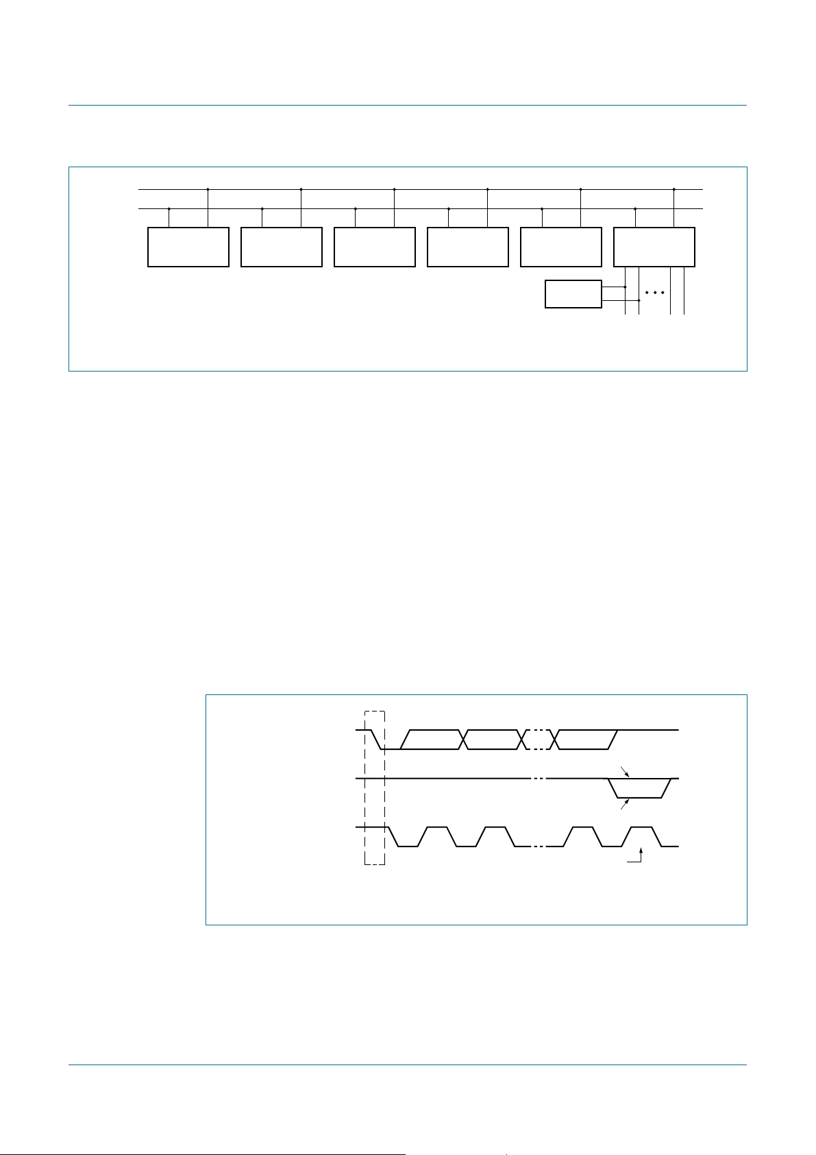
4. Block diagram
PCA9533
4-bit I2C-bus LED dimmer
PCA9533
SCL
SDA
V
DD
V
SS
INPUT
FILTERS
POWER-ON
RESET
OSCILLATOR
Remark: Only one I/O shown for clarity.
Fig 1. Block diagram of PCA9533
5. Pinning information
5.1 Pinning
I2C-BUS
CONTROL
PRESCALER 0
REGISTER
PRESCALER 1
REGISTER
PWM0
REGISTER
PWM1
REGISTER
REGISTER
LED SELECT (LSn)
REGISTER
0
1
BLINK0
BLINK1
INPUT
LEDn
002aae626
PCA9533D/01
PCA9533D/02
1
LED0 V
2
LED1 SDA
3
LED2 SCL
4
V
SS
002aae624
Fig 2. Pin configuration for SO8 Fig 3. Pin configuration for TSSOP8
5.2 Pin description
Table 3. Pin description
Symbol Pin Description
LED0 1 LED driver 0
LED1 2 LED driver 1
LED2 3 LED driver 2
V
SS
LED3 5 LED driver 3
4 supply ground
PCA9533DP/01
PCA9533DP/02
8
DD
7
6
5
LED3
1
LED0 V
2
LED1 SDA
3
LED2 SCL
4
V
SS
002aae625
8
DD
7
6
5
LED3
PCA9533_3 © NXP B.V. 2009. All rights reserved.
Product data sheet Rev. 03 — 27 April 2009 3 of 24
Page 4

NXP Semiconductors
PCA9533
4-bit I2C-bus LED dimmer
Table 3. Pin description
Symbol Pin Description
SCL 6 serial clock line
SDA 7 serial data line
V
DD
6. Functional description
Refer to Figure 1 “Block diagram of PCA9533”.
6.1 Device address
Following a START condition, the bus master must output the address of the slave it is
accessing. The address of the PCA9533/01 is shown in Figure 4 and the address of
PCA9533/02 is shown in Figure 5.
1 1 0 0 0 1 0 R/W
Fig 4. PCA9533/01 slave address Fig 5. PCA9533/02 slave address
…continued
8 supply voltage
slave address
002aae627
slave address
1 1 0 0 0 1 1 R/W
002aae628
The last bit of the address byte defines the operation to be performed. When set to logic 1
a read is selected, while a logic 0 selects a write operation.
6.2 Control register
Followingthe successful acknowledgement of the slave address, the bus master will send
a byte to the PCA9533, which will be stored in the Control register.
0 0 0 AI 0 B2 B1
register address
Reset state: 00h
Fig 6. Control register
Auto-Increment
flag
The lowest 3 bits are used as a pointer to determine which register will be accessed.
If the Auto-Increment (AI) flag is set, the three low order bits of the Control register are
automatically incremented after a read or write. This allows the user to program the
registers sequentially. The contents of these bits will rolloverto ‘000’ after the last register
is accessed.
When Auto-Increment flag is set (AI = 1) and a read sequence is initiated, the sequence
must start by reading a register different from the INPUT register (B2 B1 B0 ≠ 0 0 0).
B0
002aad744
Only the 3 least significant bits are affected by the AI flag. Unused bits must be
programmed with zeroes.
PCA9533_3 © NXP B.V. 2009. All rights reserved.
Product data sheet Rev. 03 — 27 April 2009 4 of 24
Page 5

NXP Semiconductors
6.2.1 Control register definition
Table 4. Register summary
B2 B1 B0 Symbol Access Description
0 0 0 INPUT read only input register
0 0 1 PSC0 read/write frequency prescaler 0
0 1 0 PWM0 read/write PWM register 0
0 1 1 PSC1 read/write frequency prescaler 1
1 0 0 PWM1 read/write PWM register 1
1 0 1 LS0 read/write LED selector
6.3 Register descriptions
6.3.1 INPUT - Input register
The INPUTregister reflects the state of the device pins. Writes to this register will be
acknowledged but will have no effect.
Table 5. INPUT - Input register description
Bit 7 6 5 4 3 2 1 0
Symbol ----LED3 LED2 LED1 LED0
Default 0000XXXX
PCA9533
4-bit I2C-bus LED dimmer
Remark: The default value ‘X’ is determined by the externally applied logic level(normally
logic 1) when used for directly driving LED with pull-up to VDD.
6.3.2 PCS0 - Frequency Prescaler 0
PSC0 is used to program the period of the PWM output.
The period of BLINK0 = (PSC0 + 1) / 152.
Table 6. PSC0 - Frequency Prescaler 0 register description
Bit 7 6 5 4 3 2 1 0
Symbol PSC0[7] PSC0[6] PSC0[5] PSC0[4] PSC0[3] PSC0[2] PSC0[1] PSC0[0]
Default 00000000
6.3.3 PWM0 - Pulse Width Modulation 0
The PWM0 register determines the duty cycle of BLINK0. The outputs are LOW (LED on)
when the count is less than the value in PWM0 and HIGH (LED off) when it is greater. If
PWM0 is programmed with 00h, then the PWM0 output is always HIGH (LED off).
The duty cycle of BLINK0 = PWM0 / 256.
Table 7. PWM0 - Pulse Width Modulation 0 register description
Bit 7 6 5 4 3 2 1 0
Symbol PWM0
[7]
Default 10000000
PWM0
[6]
PWM0
[5]
PWM0
[4]
PWM0
[3]
PWM0
[2]
PWM0
[1]
PWM0
[0]
PCA9533_3 © NXP B.V. 2009. All rights reserved.
Product data sheet Rev. 03 — 27 April 2009 5 of 24
Page 6

NXP Semiconductors
6.3.4 PCS1 - Frequency Prescaler 1
PSC1 is used to program the period of the PWM output.
The period of BLINK1 = (PSC1 + 1) / 152.
Table 8. PSC1 - Frequency Prescaler 1 register description
Bit 7 6 5 4 3 2 1 0
Symbol PSC1[7] PSC1[6] PSC1[5] PSC1[4] PSC1[3] PSC1[2] PSC1[1] PSC1[0]
Default 00000000
6.3.5 PWM1 - Pulse Width Modulation 1
The PWM1 register determines the duty cycle of BLINK1. The outputs are LOW (LED on)
when the count is less than the value in PWM1 and HIGH (LED off) when it is greater. If
PWM1 is programmed with 00h, then the PWM1 output is always HIGH (LED off).
The duty cycle of BLINK1 = PWM1 / 256.
Table 9. PWM1 - Pulse Width Modulation 1 register description
Bit 7 6 5 4 3 2 1 0
Symbol PWM1
Default 10000000
[7]
PWM1
[6]
PWM1
[5]
PWM1
[4]
PWM1
[3]
PCA9533
4-bit I2C-bus LED dimmer
PWM1
[2]
PWM1
[1]
PWM1
[0]
6.3.6 LS0 - LED selector
The LSn LED selector register determines the source of the LED data.
00 = output is set high-impedance (LED off; default)
01 = output is set LOW (LED on)
10 = output blinks at PWM0 rate
11 = output blinks at PWM1 rate
Table 10. LS0 - LED selector register bit description
Legend: * default value.
Register Bit Value Description
LS0 7:6 00* LED3 selected
5:4 00* LED2 selected
3:2 00* LED1 selected
1:0 00* LED0 selected
PCA9533_3 © NXP B.V. 2009. All rights reserved.
Product data sheet Rev. 03 — 27 April 2009 6 of 24
Page 7

NXP Semiconductors
6.4 Pins used as GPIOs
LEDn pins not used to control LEDs can be used as General Purpose I/Os (GPIOs).
For use as input, set LEDn to high-impedance (00) and then read the pin state via the
INPUT register.
For use as output, connect external pull-up resistor to the pin and size it according to the
DC recommended operating characteristics. LEDn output pin is HIGH when the output is
programmed as high-impedance, and LOW when the output is programmedLOW through
the ‘LED selector’ register. The output can be pulse-width controlled when PWM0 or
PWM1 are used.
6.5 Power-on reset
When power is applied to VDD, an internal Power-On Reset (POR) holds the PCA9533 in
a reset condition until VDDhas reached V
and the PCA9533 registers are initialized to their default states, all the outputs in the
OFF state. Thereafter, VDD must be lowered below 0.2 V to reset the device.
PCA9533
4-bit I2C-bus LED dimmer
. At that point, the reset condition is released
POR
PCA9533_3 © NXP B.V. 2009. All rights reserved.
Product data sheet Rev. 03 — 27 April 2009 7 of 24
Page 8

NXP Semiconductors
7. Characteristics of the I2C-bus
The I2C-bus is for 2-way, 2-line communication between different ICs or modules. The two
lines are a serial data line (SDA) and a serial clock line (SCL). Both lines must be
connected to a positive supply via a pull-up resistor when connected to the output stages
of a device. Data transfer may be initiated only when the bus is not busy.
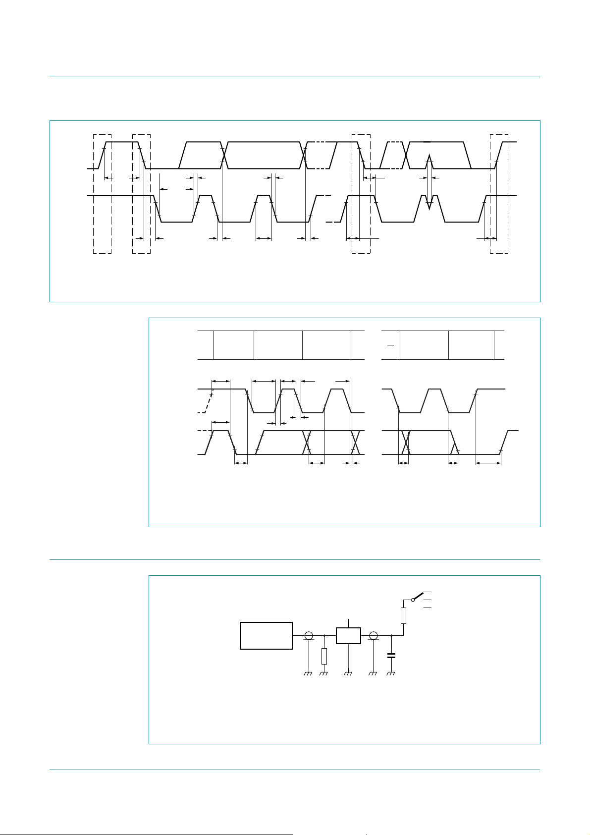
7.1 Bit transfer
One data bit is transferred during each clock pulse. The data on the SDA line must remain
stable during the HIGH period of the clock pulse as changes in the data line at this time
will be interpreted as control signals (see Figure 7).
SDA
SCL
PCA9533
4-bit I2C-bus LED dimmer
Fig 7. Bit transfer
7.1.1 START and STOP conditions
Both data and clock lines remain HIGH when the bus is not busy. A HIGH-to-LOW
transition of the data line while the clock is HIGH is defined as the START condition (S).
A LOW-to-HIGH transition of the data line while the clock is HIGH is defined as the STOP
condition (P) (see Figure 8).
SDA
SCL
S
START condition
Fig 8. Definition of START and STOP conditions
7.2 System configuration
data line
stable;
data valid
change
of data
allowed
mba607
P
STOP condition
mba608
A device generating a message is a ‘transmitter’; a device receiving is the ‘receiver’. The
device that controls the message is the ‘master’ and the devices which are controlled by
the master are the ‘slaves’ (see Figure 9).
PCA9533_3 © NXP B.V. 2009. All rights reserved.
Product data sheet Rev. 03 — 27 April 2009 8 of 24
Page 9
NXP Semiconductors
SDA
SCL
PCA9533
4-bit I2C-bus LED dimmer
MASTER
TRANSMITTER/
RECEIVER
Fig 9. System configuration
7.3 Acknowledge
The number of data bytes transferred between the START and the STOP conditions from
transmitter to receiver is not limited. Each byte of eight bits is followed by one
acknowledge bit. The acknowledge bit is a HIGH level put on the bus by the transmitter,
whereas the master generates an extra acknowledge related clock pulse.
A slavereceiver which is addressed must generate an acknowledge after the reception of
each byte. Also a master must generate an acknowledge after the reception of each byte
that has been clocked out of the slave transmitter. The device that acknowledges has to
pull down the SDA line during the acknowledge clock pulse, so that the SDA line is stable
LOW during the HIGH period of the acknowledge related clock pulse; set-up and hold
times must be taken into account.
A master receiver must signal an end of data to the transmitter by not generating an
acknowledge on the last byte that has been clocked out of the slave. In this event, the
transmitter must leave the data line HIGH to enable the master to generate a STOP
condition.
SLAVE
RECEIVER
SLAVE
TRANSMITTER/
RECEIVER
MASTER
TRANSMITTER
MASTER
TRANSMITTER/
RECEIVER
SLAVE
I2C-BUS
MULTIPLEXER
002aaa966
data output
by transmitter
not acknowledge
data output
by receiver
acknowledge
SCL from master
S
START
condition
clock pulse for
acknowledgement
9821
002aaa987
Fig 10. Acknowledgement on the I2C-bus
PCA9533_3 © NXP B.V. 2009. All rights reserved.
Product data sheet Rev. 03 — 27 April 2009 9 of 24
Page 10

NXP Semiconductors
7.4 Bus transactions
12345678SCL 9
PCA9533
4-bit I2C-bus LED dimmer
slave address (PCA9533/01)
SDA DATA 1 A
write to register
data out from port
1000101
START condition R/W acknowledge
Fig 11. Write to register
slave address (PCA9533/01)
SDA
(cont.)
1000100AS1
START condition R/W
slave address (PCA9533/01)
S
1000101
(repeated)
START condition
0 AS
acknowledge
from slave
R/W
acknowledge
from slave
command byte
0 0 AI 0 B2B1B00
from slave
command byte
0 0 AI 0 B2 B10B0
acknowledge
from slave
data from register
1 A
DATA (first byte)
Auto-Increment
register address
if AI = 1
at this moment master-transmitter becomes master-receiver
and slave-receiver becomes slave-transmitter
A
acknowledge
from slave
A
A P
data to register
(cont.)
acknowledge
from master
t
v(Q)
data from register
DATA (last byte)
no acknowledge
acknowledge
from slave
DATA 1 VALID
from master
002aae629
NA
STOP
condition
002aae630
Fig 12. Read from register
no acknowledge
from master
slave address (PCA9533/01)
SDA NA
read from
port
data into
port
1000101AS1
START condition R/W acknowledge
DATA 1
t
h(D)
from slave
data from port
t
su(D)
A
acknowledge
from master
DATA 1
DATA 2 DATA 3 DATA 4
data from port
DATA 4
P
STOP
condition
002aae631
Remark: This figure assumes the command byte has previously been programmed with 00h.
Fig 13. Read input port register
PCA9533_3 © NXP B.V. 2009. All rights reserved.
Product data sheet Rev. 03 — 27 April 2009 10 of 24
Page 11

NXP Semiconductors
8. Application design-in information
PCA9533
4-bit I2C-bus LED dimmer
5 V
2
C-BUS/SMBus
I
MASTER
SDA
SCL
10 kΩ10 kΩ
V
DD
SDA
SCL
LED0
LED1
LED2
LED3
5 V
PCA9533
V
SS
002aae632
Fig 14. Typical application
8.1 Minimizing IDD when the I/Os are used to control LEDs
When the I/Os are used to control LEDs, they are normally connected to VDD through a
resistor as shown in Figure 14. Since the LED acts as a diode, when the LED is off the
I/O VI is about 1.2 V less than VDD. The supply current, IDD, increases as VI becomes
lower than VDD and is specified as ∆IDD in Table 13 “Static characteristics”.
Designs needing to minimize current consumption, such as battery power applications,
should consider maintaining the I/O pins greater than or equal to VDDwhen the LED is off.
Figure 15 shows a high value resistor in parallel with the LED. Figure 16 shows VDD less
than the LED supply voltage by at least 1.2 V. Both of these methods maintain the I/O V
at or above VDD and prevents additional supply current consumption when the LED is off.
I
V
DD
V
DD
LEDn
LED
100 kΩ
002aac189
Fig 15. High value resistor in parallel with
Fig 16. Device supplied by a lower voltage
3.3 V 5 V
V
DD
LEDn
002aac190
LED
the LED
PCA9533_3 © NXP B.V. 2009. All rights reserved.
Product data sheet Rev. 03 — 27 April 2009 11 of 24
Page 12

NXP Semiconductors
8.2 Programming example
The followingexample will show how to set LED0 and LED1 off. It will set LED2 to blink at
1 Hz at a 50 % duty cycle. LED3 will be set to be dimmed at 25 % of their maximum
brightness (duty cycle = 25 %). PCA9533/01 is used in this example.
Table 11. Programming PCA9533
Program sequence I2C-bus
START S
PCA9533 address C4h
PSC0 subaddress + Auto-Increment 11h
Set prescaler PSC0 to achieve a period of 1 second:
Blink period 1
PSC0 = 151
Set PWM0 duty cycle to 50 %:
PWM0
-----------------
PWM0 = 128
Set prescaler PCS1 to dim at maximum frequency:
256
0.5=
PSC0 1+
==
----------------------- -
PCA9533
4-bit I2C-bus LED dimmer
97h
152
80h
00h
Blink period max=
PSC1 = 0
Set PWM1 output duty cycle to 25 %:
PWM1
-----------------
PWM1 = 64
Set LED0 on, LED1 off; LED2 set to blink at PSC0, PWM0; LED3 set to blink at
PSC1, PWM1
STOP P
9. Limiting values
Table 12. Limiting values
In accordance with the Absolute Maximum Rating System (IEC 60134).
Symbol Parameter Conditions Min Max Unit
V
DD
V
I/O
I
O(LEDn)
I
SS
P
tot
T
stg
T
amb
256
40h
0.25=
E1h
supply voltage −0.5 +6.0 V
voltage on an input/output pin VSS− 0.5 5.5 V
output current on pin LEDn - 25 mA
ground supply current - 100 mA
total power dissipation - 400 mW
storage temperature −65 +150 °C
ambient temperature operating −40 +85 °C
PCA9533_3 © NXP B.V. 2009. All rights reserved.
Product data sheet Rev. 03 — 27 April 2009 12 of 24
Page 13

NXP Semiconductors
4-bit I2C-bus LED dimmer
10. Static characteristics
Table 13. Static characteristics
VDD= 2.3 V to 5.5 V; VSS=0V; T
Symbol Parameter Conditions Min Typ
Supplies
V
I
I
∆I
DD
DD
stb
DD
supply voltage 2.3 - 5.5 V
supply current operating mode; VDD= 5.5 V; no load;
standby current Standby mode; VDD= 5.5 V; no load;
additional quiescent supply
current
V
POR
power-on reset voltage no load; VI=VDD or V
Input SCL; input/output SDA
V
IL
V
IH
I
OL
I
L
C
i
LOW-level input voltage −0.5 - +0.3V
HIGH-level input voltage 0.7V
LOW-level output current VOL= 0.4 V 3 6.5 - mA
leakage current VI=VDD=V
input capacitance VI=V
I/Os
V
IL
V
IH
I
OL
I
LI
C
io
LOW-level input voltage −0.5 - +0.8 V
HIGH-level input voltage 2.0 - 5.5 V
LOW-level output current VOL= 0.4 V
input leakage current VDD= 3.6 V; VI= 0 V or V
input/output capacitance - 2.1 5 pF
=−40°C to +85°C; unless otherwise specified.
amb
V
V
I=VDD
I=VDD
or VSS; f
or VSS; f
= 100 kHz
SCL
= 0 kHz
SCL
Standby mode; VDD= 5.5 V;
every LED I/O at V
f
= 0 kHz
SCL
SS
= 2.3 V
V
DD
= 3.0 V
V
DD
= 5.0 V
V
DD
= 0.7 V
V
OL
= 2.3 V
V
DD
= 3.0 V
V
DD
= 5.0 V
V
DD
SS
= 4.3 V;
I
SS
DD
- 350 550 µA
- 1.9 3.0 µA
- - 325 µA
[2]
- 1.7 2.2 V
- 5.5 V
DD
−1- +1 µA
- 3.7 5 pF
[3]
9-- mA
[3]
12 - - mA
[3]
15 - - mA
[3]
15 - - mA
[3]
20 - - mA
[3]
25 - - mA
−1- +1 µA
PCA9533
[1]
Max Unit
DD
V
[1] Typical limits at VDD= 3.3 V, T
[2] VDD must be lowered to 0.2 V in order to reset part.
[3] Each I/O must be externally limited to a maximum of 25 mA and the device must be limited to a maximum current of 100 mA.
PCA9533_3 © NXP B.V. 2009. All rights reserved.
Product data sheet Rev. 03 — 27 April 2009 13 of 24
amb
=25°C.
Page 14

NXP Semiconductors
PCA9533
4-bit I2C-bus LED dimmer
20 %
percent
variation
0 %
−20 %
−40 %
(1)
(2)
(3)
−40 100−20
0 20406080
002aac191
T
amb
(°C)
(1) maximum
(2) average
(3) minimum
Fig 17. Typical frequency variation over process at
V
= 2.3 V to 3.0 V
DD
20 %
percent
variation
0 %
−20 %
−40 %
(1)
(2)
(3)
−40 100−20
0 20406080
002aac192
T
(°C)
amb
(1) maximum
(2) average
(3) minimum
Fig 18. Typical frequency variation over process at
VDD= 3.0 V to 5.5 V
PCA9533_3 © NXP B.V. 2009. All rights reserved.
Product data sheet Rev. 03 — 27 April 2009 14 of 24
Page 15

NXP Semiconductors
11. Dynamic characteristics
Table 14. Dynamic characteristics
Symbol Parameter Conditions Standard-mode
f
SCL
t
BUF
SCL clock frequency 0 100 0 400 kHz
bus free time between a STOP and
START condition
t
HD;STA
t
SU;STA
hold time (repeated) START condition 4.0 - 0.6 - µs
set-up time for a repeated START
condition
t
SU;STO
t
HD;DAT
t
VD;ACK
t
VD;DAT
t
SU;DAT
t
LOW
t
HIGH
t
r
t
f
t
SP
set-up time for STOP condition 4.0 - 0.6 - µs
data hold time 0 - 0 - ns
data valid acknowledge time
data valid time LOW-level
HIGH-level
[1]
[2]
[2]
data set-up time 250 - 100 - ns
LOW period of the SCL clock 4.7 - 1.3 - µs
HIGH period of the SCL clock 4.0 - 0.6 - µs
rise time of both SDA and SCL signals - 1000 20 + 0.1C
fall time of both SDA and SCL signals - 300 20 + 0.1C
pulse width of spikes that must be
suppressed by the input filter
Port timing
t
v(Q)
t
su(D)
t
h(D)
data output valid time - 200 - 200 ns
data input set-up time 100 - 100 - ns
data input hold time 1 - 1 - µs
2
I
C-bus
Min Max Min Max
4.7 - 1.3 - µs
4.7 - 0.6 - µs
- 600 - 600 ns
- 600 - 600 ns
- 1500 - 600 ns
- 50 - 50 ns
PCA9533
4-bit I2C-bus LED dimmer
Fast-mode I2C-bus Unit
[3]
300 ns
b
[3]
300 ns
b
[1] t
[2] t
[3] Cb= total capacitance of one bus line in pF.
PCA9533_3 © NXP B.V. 2009. All rights reserved.
Product data sheet Rev. 03 — 27 April 2009 15 of 24
= time for Acknowledgement signal from SCL LOW to SDA (out) LOW.
VD;ACK
= minimum time for SDA data output to be valid following SCL LOW.
VD;DAT
Page 16
NXP Semiconductors
SDA
PCA9533
4-bit I2C-bus LED dimmer
t
BUF
SCL
t
Fig 19. Definition of timing
t
LOW
HD;STA
protocol
SCL
SDA
t
r
t
HD;DAT
condition
t
SU;STA
t
BUF
START
(S)
t
HIGH
bit 7
MSB
(A7)
t
LOWtHIGH
t
r
t
f
t
SU;DAT
(A)
t
SP
t
SU;STO
STOP
condition
PP S
002aaa986
(P)
t
HD;STA
t
SU;STA
Sr
bit 6
(A6)
1
/f
SCL
t
f
bit 0
(R/W)
acknowledge
Fig 20. I2C-bus timing diagram
12. Test information
Fig 21. Test circuitry for switching times
t
HD;STA
t
SU;DAT
t
HD;DAT
t
VD;DAT
t
VD;ACK
t
SU;STO
002aab175
Rise and fall times refer to VIL and VIH.
V
DD
open
V
L
002aab880
SS
PULSE
GENERATOR
V
DD
V
I
V
O
R
500 Ω
DUT
C
R
T
L
50 pF
RL = load resistor for LEDn. RL for SDA and SCL > 1kΩ (3 mA or less current).
CL = load capacitance includes jig and probe capacitance.
RT = termination resistance should be equal to the output impedance Zo of the pulse generators.
PCA9533_3 © NXP B.V. 2009. All rights reserved.
Product data sheet Rev. 03 — 27 April 2009 16 of 24
Page 17
NXP Semiconductors
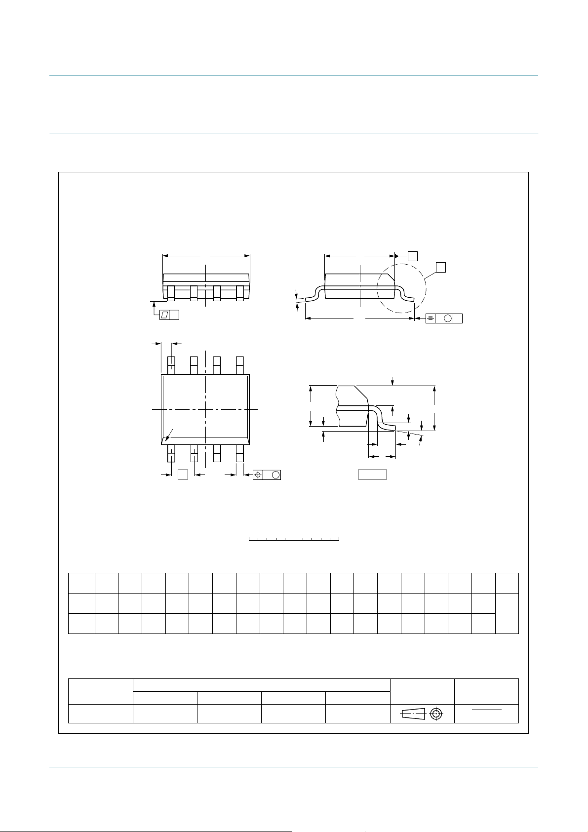
13. Package outline
PCA9533
4-bit I2C-bus LED dimmer
SO8: plastic small outline package; 8 leads; body width 3.9 mm
D
c
y
Z
8
pin 1 index
1
e
5
A
2
A
4
w M
b
p
SOT96-1
E
H
E
1
detail X
A
X
v M
A
Q
A
(A )
3
θ
L
p
L
0 2.5 5 mm
scale
DIMENSIONS (inch dimensions are derived from the original mm dimensions)
mm
OUTLINE
VERSION
SOT96-1
A
A1A2A3b
max.
0.25
1.75
0.10
0.010
0.069
0.004
p
1.45
1.25
0.057
0.049
IEC JEDEC JEITA
076E03 MS-012
0.25
0.01
0.49
0.36
0.019
0.014
0.25
0.19
0.0100
0.0075
UNIT
inches
Notes
1. Plastic or metal protrusions of 0.15 mm (0.006 inch) maximum per side are not included.
2. Plastic or metal protrusions of 0.25 mm (0.01 inch) maximum per side are not included.
(1)E(2)
cD
5.0
4.8
0.20
0.19
REFERENCES
eHELLpQZywv θ
4.0
3.8
0.16
0.15
1.27
0.05
6.2
5.8
0.244
0.228
1.05
1.0
0.4
0.039
0.016
0.7
0.6
0.028
0.024
0.25 0.10.25
0.010.010.041 0.004
EUROPEAN
PROJECTION
(1)
0.7
0.3
0.028
0.012
ISSUE DATE
99-12-27
03-02-18
o
8
o
0
Fig 22. Package outline SOT96-1 (SO8)
PCA9533_3 © NXP B.V. 2009. All rights reserved.
Product data sheet Rev. 03 — 27 April 2009 17 of 24
Page 18
NXP Semiconductors
PCA9533
4-bit I2C-bus LED dimmer
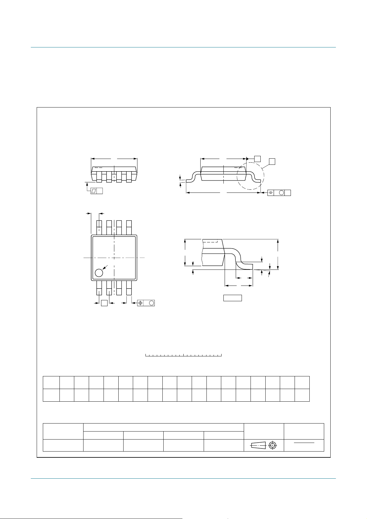
TSSOP8: plastic thin shrink small outline package; 8 leads; body width 3 mm
D
y
Z
8
pin 1 index
5
14
e
w M
b
p
c
A
2
A
1
E
H
E
detail X
SOT505-1
A
X
v M
A
(A3)
L
p
L
A
θ
2.5 5 mm0
scale
DIMENSIONS (mm are the original dimensions)
A
A
UNIT
max.
mm
1.1
Notes
1. Plastic or metal protrusions of 0.15 mm maximum per side are not included.
2. Plastic or metal protrusions of 0.25 mm maximum per side are not included.
OUTLINE
VERSION
SOT505-1
1
0.15
0.05
A2A3b
0.95
0.25
0.80
IEC JEDEC JEITA
p
0.45
0.25
ceD
0.28
0.15
REFERENCES
(1)E(2)
3.1
2.9
3.1
2.9
0.65
5.1
4.7
LH
E
L
0.7
0.4
p
wyv
0.1 0.10.10.94
EUROPEAN
PROJECTION
(1)
Z
0.70
0.35
ISSUE DATE
99-04-09
03-02-18
θ
6°
0°
Fig 23. Package outline SOT505-1 (TSSOP8)
PCA9533_3 © NXP B.V. 2009. All rights reserved.
Product data sheet Rev. 03 — 27 April 2009 18 of 24
Page 19

NXP Semiconductors
14. Handling information
All input and output pins are protected against ElectroStatic Discharge (ESD) under
normal handling. When handling ensure that the appropriate precautions are taken as
described in
JESD625-A
15. Soldering of SMD packages
This text provides a very brief insight into a complex technology. A more in-depth account
of soldering ICs can be found in Application Note
soldering description”
15.1 Introduction to soldering
Soldering is one of the most common methods through which packages are attached to
Printed Circuit Boards (PCBs), to form electrical circuits. The soldered joint provides both
the mechanical and the electrical connection. There is no single soldering method that is
ideal for all IC packages. Wave soldering is often preferred when through-hole and
Surface Mount Devices (SMDs) are mixed on one printed wiring board; however, it is not
suitable for fine pitch SMDs. Reflow soldering is ideal for the small pitches and high
densities that come with increased miniaturization.
.
PCA9533
4-bit I2C-bus LED dimmer
or equivalent standards.
AN10365 “Surface mount reflow
15.2 Wave and reflow soldering
Wave soldering is a joining technology in which the joints are made by solder coming from
a standing wave of liquid solder. The wave soldering process is suitable for the following:
• Through-hole components
• Leaded or leadless SMDs, which are glued to the surface of the printed circuit board
Not all SMDs can be wave soldered. Packages with solder balls, and some leadless
packages which have solder lands underneath the body, cannot be wave soldered. Also,
leaded SMDs with leads having a pitch smaller than ~0.6 mm cannot be wave soldered,
due to an increased probability of bridging.
The reflow soldering process involves applying solder paste to a board, followed by
component placement and exposure to a temperature profile. Leaded packages,
packages with solder balls, and leadless packages are all reflow solderable.
Key characteristics in both wave and reflow soldering are:
• Board specifications, including the board finish, solder masks and vias
• Package footprints, including solder thieves and orientation
• The moisture sensitivity level of the packages
• Package placement
• Inspection and repair
• Lead-free soldering versus SnPb soldering
15.3 Wave soldering
Key characteristics in wave soldering are:
PCA9533_3 © NXP B.V. 2009. All rights reserved.
Product data sheet Rev. 03 — 27 April 2009 19 of 24
Page 20

NXP Semiconductors
• Process issues, such as application of adhesive and flux, clinching of leads, board
• Solder bath specifications, including temperature and impurities
15.4 Reflow soldering
Key characteristics in reflow soldering are:
• Lead-freeversusSnPb soldering; note that a lead-free reflow process usually leads to
• Solder paste printing issues including smearing, release, and adjusting the process
• Reflow temperature profile; this profile includes preheat, reflow (in which the board is
PCA9533
4-bit I2C-bus LED dimmer
transport, the solder wave parameters, and the time during which components are
exposed to the wave
higher minimum peak temperatures (see Figure 24) than a SnPb process, thus
reducing the process window
window for a mix of large and small components on one board
heated to the peak temperature) and cooling down. It is imperative that the peak
temperature is high enough forthe solder to make reliable solder joints (a solder paste
characteristic). In addition, the peak temperature must be low enough that the
packages and/or boards are not damaged. The peak temperature of the package
depends on package thickness and volume and is classified in accordance with
Table 15 and 16
Table 15. SnPb eutectic process (from J-STD-020C)
Package thickness (mm) Package reflow temperature (°C)
Volume (mm3)
< 350 ≥ 350
< 2.5 235 220
≥ 2.5 220 220
Table 16. Lead-free process (from J-STD-020C)
Package thickness (mm) Package reflow temperature (°C)
Volume (mm3)
< 350 350 to 2000 > 2000
< 1.6 260 260 260
1.6 to 2.5 260 250 245
> 2.5 250 245 245
Moisture sensitivity precautions, as indicated on the packing, must be respected at all
times.
Studies have shown that small packages reach higher temperatures during reflow
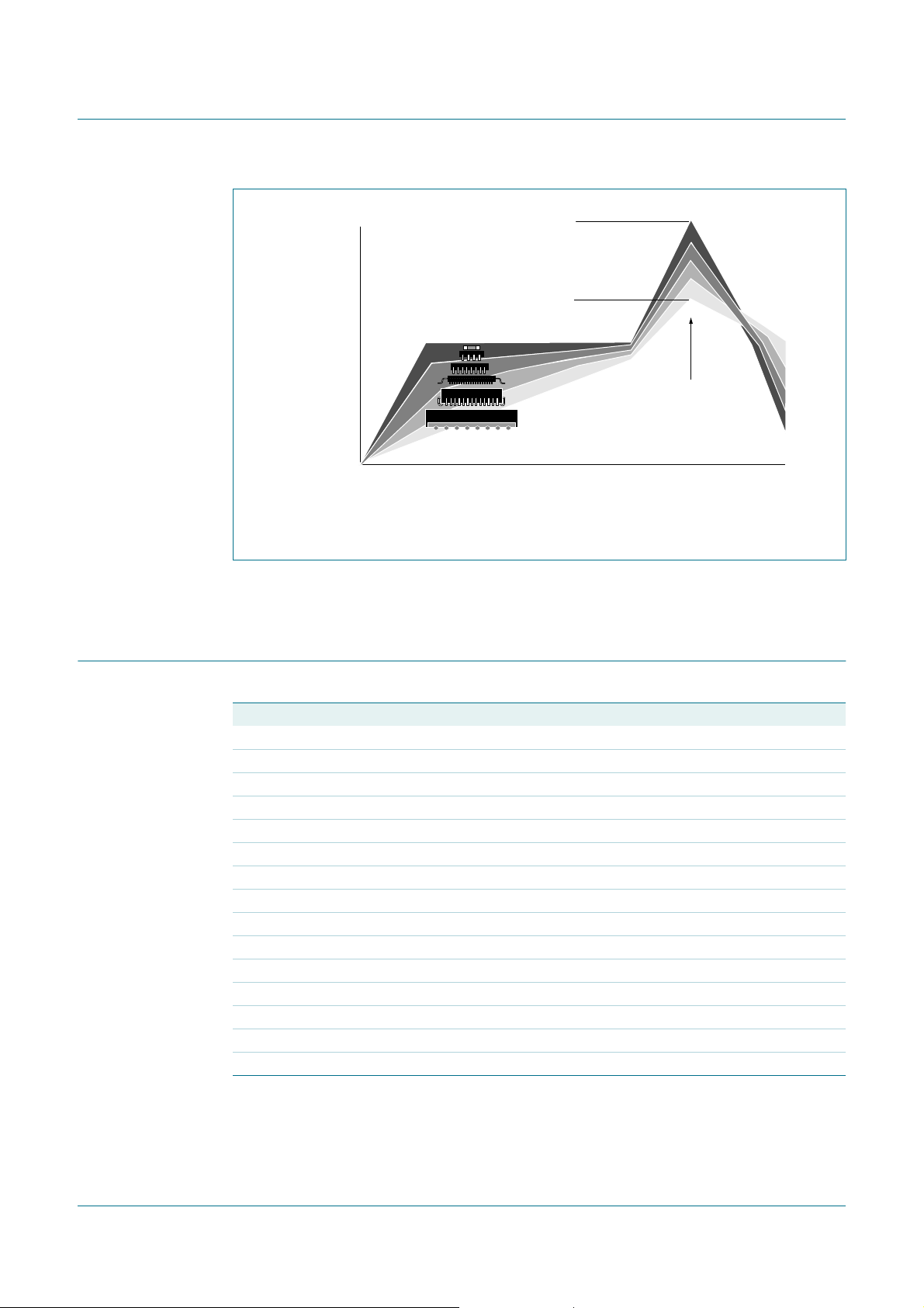
soldering, see Figure 24.
PCA9533_3 © NXP B.V. 2009. All rights reserved.
Product data sheet Rev. 03 — 27 April 2009 20 of 24
Page 21
NXP Semiconductors
Fig 24. Temperature profiles for large and small components
maximum peak temperature
temperature
MSL: Moisture Sensitivity Level
= MSL limit, damage level
minimum peak temperature
= minimum soldering temperature
PCA9533
4-bit I2C-bus LED dimmer
peak
temperature
time
001aac844
For further information on temperature profiles, refer to Application Note
“Surface mount reflow soldering description”
16. Abbreviations
Table 17. Abbreviations
Acronym Description
ACPI Advanced Configuration and Power Interface
CDM Charged Device Model
DSP Digital Signal Processor
DUT Device Under Test
ESD ElectroStatic Discharge
GPIO General Purpose Input/Output
HBM Human Body Model
2
C-bus Inter-Integrated Circuit bus
I
LED Light Emitting Diode
MCU MicroController Unit
MM Machine Model
MPU MicroProcessor Unit
POR Power-On Reset
RC Resistor-Capacitor network
SMBus System Management Bus
AN10365
.
PCA9533_3 © NXP B.V. 2009. All rights reserved.
Product data sheet Rev. 03 — 27 April 2009 21 of 24
Page 22

NXP Semiconductors
PCA9533
4-bit I2C-bus LED dimmer
17. Revision history
Table 18. Revision history
Document ID Release date Data sheet status Change notice Supersedes
PCA9533_3 20090427 Product data sheet - PCA9533_2
Modifications:
PCA9533_2
(9397 750 13692)
PCA9533_1
(9397 750 12061)
• The format of this data sheet has been redesigned to comply with the new identity guidelines of
NXP Semiconductors.
• Legal texts have been adapted to the new company name where appropriate.
• Figure 11 “Write to register”: changed symbol from “t
pv
” to “t
v(Q)
”
• Figure 13 “Read input port register”:
– changed symbol from “t
– changed symbol from “t
ph
ps
” to “t
” to “t
• Table 11 “Programming PCA9533”,6
at maximum frequency” to “Set prescaler PSC1 to dim at maximum frequency”
• Table 12 “Limiting values”: changed symbol/parameter from “I
to “I
, output current on pin LEDn”
O(LEDn)
”
h(D)
”
su(D)
th
table body row: changed from “Set prescaler PWM1 to dim
, DC output current on an I/O”
I/O
• Table 13 “Static characteristics”:
– descriptive line below table title: phrase “TYP at 3.3 V and 25 °C” is re-written as
with reference to it at column heading “Typ”
– sub-section “I/Os”: symbol for parameter “input leakage current” changed from “I
Table note [1],
” to “ILI”
L
• Table 14 “Dynamic characteristics”:
– symbols t
Conditions
– symbol/parameter changed from “t
– symbol/parameter changed from “t
– symbol/parameter changed from “t
VD;DAT
(L) and t
(H) are merged as “t
VD;DAT
, Output data valid” to “t
PV
, Input data setup time” to “t
PS
, Input data hold time” to “t
PH
”; LOW and HIGH levels noted under
VD;DAT
, data output valid time”
v(Q)
, data input set-up time”
su(D)
, data input hold time”
h(D)
• Added soldering information
• Added Section 16 “Abbreviations”
20041001 Product data sheet - PCA9533_1
20030919 Product data ECN 853-2404 30307
dated 08 Sep 2003
-
PCA9533_3 © NXP B.V. 2009. All rights reserved.
Product data sheet Rev. 03 — 27 April 2009 22 of 24
Page 23

NXP Semiconductors
18. Legal information
18.1 Data sheet status
PCA9533
4-bit I2C-bus LED dimmer
Document status
Objective [short] data sheet Development This document contains data from the objective specification for product development.
Preliminary [short] data sheet Qualification This document contains data from the preliminary specification.
Product [short] data sheet Production This document contains the product specification.
[1] Please consult the most recently issued document before initiating or completing a design.
[2] The term ‘short data sheet’ is explained in section “Definitions”.
[3] Theproduct status of device(s) describedin this documentmay havechanged since thisdocument was publishedand maydiffer in caseof multiple devices. The latestproduct status
information is available on the Internet at URL
[1][2]
Product status
18.2 Definitions
Draft — The document is a draft version only. The content is still under
internal review and subject to formal approval, which may result in
modifications or additions. NXP Semiconductors does not give any
representations or warranties as to the accuracy or completeness of
information includedherein and shall haveno liability fortheconsequences of
use of such information.
Short data sheet — A short data sheet is an extract from a full data sheet
with thesame product type number(s) andtitle. A short data sheetis intended
for quickreference only and should not be reliedupon to contain detailed and
full information. For detailed and full information see the relevant full data
sheet, which is available on request via the local NXP Semiconductors sales
office. In case of any inconsistency or conflict with the short data sheet, the
full data sheet shall prevail.
18.3 Disclaimers
General — Information in this document is believed to be accurate and
reliable. However,NXPSemiconductors does not give any representationsor
warranties, expressedor implied, as to the accuracyor completeness of such
information and shall have no liability for the consequences of use of such
information.
Right to make changes — NXP Semiconductors reserves the right to make
changes to information published in this document, including without
limitation specifications and product descriptions, at any time and without
notice. This documentsupersedesand replaces all information supplied prior
to the publication hereof.
Suitability for use — NXP Semiconductors products are not designed,
authorized or warranted to be suitable for use in medical, military, aircraft,
space or life support equipment, nor in applications where failure or
malfunction of an NXP Semiconductors product can reasonably be expected
to result in personal injury, death or severe property or environmental
[3]
http://www.nxp.com.
Definition
damage. NXP Semiconductors accepts no liability for inclusion and/or use of
NXP Semiconductors products in such equipment or applications and
therefore such inclusion and/or use is at the customer’s own risk.
Applications — Applications that are described herein for any of these
products are for illustrative purposes only. NXP Semiconductors makes no
representation or warranty that such applications will be suitable for the
specified use without further testing or modification.
Limiting values — Stress above one or more limiting values (as defined in
the Absolute MaximumRatings System of IEC 60134) may cause permanent
damage to thedevice. Limiting valuesarestress ratings only and operationof
the device at these or any other conditions above those given in the
Characteristics sections of this document is not implied. Exposure to limiting
values for extended periods may affect device reliability.
Terms and conditions of sale — NXP Semiconductors products are sold
subject to the general terms and conditions of commercial sale, as published
at
http://www.nxp.com/profile/terms, including those pertaining to warranty,
intellectual property rights infringement and limitation of liability, unless
explicitly otherwise agreed to in writing by NXP Semiconductors. In case of
any inconsistency or conflict between information in this document and such
terms and conditions, the latter will prevail.
No offer to sell or license — Nothing in this document may be interpreted
or construed as an offer to sell products that is open for acceptance or the
grant, conveyance or implication of any license underanycopyrights, patents
or other industrial or intellectual property rights.
Export control — This document as well as the item(s) described herein
may be subject to export control regulations. Export might require a prior
authorization from national authorities.
18.4 Trademarks
Notice: Allreferenced brands, productnames, service names andtrademarks
are the property of their respective owners.
I2C-bus — logo is a trademark of NXP B.V.
19. Contact information
For more information, please visit: http://www.nxp.com
For sales office addresses, please send an email to: salesaddresses@nxp.com
PCA9533_3 © NXP B.V. 2009. All rights reserved.
Product data sheet Rev. 03 — 27 April 2009 23 of 24
Page 24

NXP Semiconductors
20. Contents
PCA9533
4-bit I2C-bus LED dimmer
1 General description. . . . . . . . . . . . . . . . . . . . . . 1
2 Features . . . . . . . . . . . . . . . . . . . . . . . . . . . . . . . 1
3 Ordering information. . . . . . . . . . . . . . . . . . . . . 2
3.1 Ordering options . . . . . . . . . . . . . . . . . . . . . . . . 2
4 Block diagram . . . . . . . . . . . . . . . . . . . . . . . . . . 3
5 Pinning information. . . . . . . . . . . . . . . . . . . . . . 3
5.1 Pinning . . . . . . . . . . . . . . . . . . . . . . . . . . . . . . . 3
5.2 Pin description . . . . . . . . . . . . . . . . . . . . . . . . . 3
6 Functional description . . . . . . . . . . . . . . . . . . . 4
6.1 Device address. . . . . . . . . . . . . . . . . . . . . . . . . 4
6.2 Control register . . . . . . . . . . . . . . . . . . . . . . . . . 4
6.2.1 Control register definition . . . . . . . . . . . . . . . . . 5
6.3 Register descriptions . . . . . . . . . . . . . . . . . . . . 5
6.3.1 INPUT - Input register. . . . . . . . . . . . . . . . . . . . 5
6.3.2 PCS0 - Frequency Prescaler 0. . . . . . . . . . . . . 5
6.3.3 PWM0 - Pulse Width Modulation 0. . . . . . . . . . 5
6.3.4 PCS1 - Frequency Prescaler 1. . . . . . . . . . . . . 6
6.3.5 PWM1 - Pulse Width Modulation 1. . . . . . . . . . 6
6.3.6 LS0 - LED selector . . . . . . . . . . . . . . . . . . . . . . 6
6.4 Pins used as GPIOs . . . . . . . . . . . . . . . . . . . . . 7
6.5 Power-on reset . . . . . . . . . . . . . . . . . . . . . . . . . 7
7 Characteristics of the I
2
C-bus. . . . . . . . . . . . . . 8
7.1 Bit transfer . . . . . . . . . . . . . . . . . . . . . . . . . . . . 8
7.1.1 START and STOP conditions . . . . . . . . . . . . . . 8
7.2 System configuration . . . . . . . . . . . . . . . . . . . . 8
7.3 Acknowledge . . . . . . . . . . . . . . . . . . . . . . . . . . 9
7.4 Bus transactions . . . . . . . . . . . . . . . . . . . . . . . 10
8 Application design-in information . . . . . . . . . 11
8.1 Minimizing I
when the I/Os are used to
DD
control LEDs. . . . . . . . . . . . . . . . . . . . . . . . . . 11
8.2 Programming example . . . . . . . . . . . . . . . . . . 12
9 Limiting values. . . . . . . . . . . . . . . . . . . . . . . . . 12
10 Static characteristics. . . . . . . . . . . . . . . . . . . . 13
11 Dynamic characteristics . . . . . . . . . . . . . . . . . 15
12 Test information. . . . . . . . . . . . . . . . . . . . . . . . 16
13 Package outline . . . . . . . . . . . . . . . . . . . . . . . . 17
14 Handling information. . . . . . . . . . . . . . . . . . . . 19
15 Soldering of SMD packages . . . . . . . . . . . . . . 19
15.1 Introduction to soldering. . . . . . . . . . . . . . . . . 19
15.2 Wave and reflow soldering . . . . . . . . . . . . . . . 19
15.3 Wave soldering. . . . . . . . . . . . . . . . . . . . . . . . 19
15.4 Reflow soldering. . . . . . . . . . . . . . . . . . . . . . . 20
16 Abbreviations. . . . . . . . . . . . . . . . . . . . . . . . . . 21
17 Revision history. . . . . . . . . . . . . . . . . . . . . . . . 22
18 Legal information . . . . . . . . . . . . . . . . . . . . . . 23
18.1 Data sheet status. . . . . . . . . . . . . . . . . . . . . . 23
18.2 Definitions . . . . . . . . . . . . . . . . . . . . . . . . . . . 23
18.3 Disclaimers. . . . . . . . . . . . . . . . . . . . . . . . . . . 23
18.4 Trademarks . . . . . . . . . . . . . . . . . . . . . . . . . . 23
19 Contact information . . . . . . . . . . . . . . . . . . . . 23
20 Contents. . . . . . . . . . . . . . . . . . . . . . . . . . . . . . 24
Please be aware that important notices concerning this document and the product(s)
described herein, have been included in section ‘Legal information’.
© NXP B.V. 2009. All rights reserved.
For more information, please visit: http://www.nxp.com
For sales office addresses, please send an email to: salesaddresses@nxp.com
Date of release: 27 April 2009
Document identifier: PCA9533_3
 Loading...