

Page 1

PCA9517
Level translating I2C-bus repeater
Rev. 03 — 30 January 2007 Product data sheet
1. General description
The PCA9517 is a CMOS integrated circuit that provides level shifting between low
voltage(down to 0.9 V) and higher voltage(2.7 V to 5.5 V) I2C-bus or SMBus applications.
While retaining all the operating modes and features of the I2C-bus system during the
level shifts, it also permits extension of the I2C-bus by providing bidirectional buffering for
both the data (SDA) and the clock (SCL) lines, thus enabling two buses of 400 pF. Using
the PCA9517 enables the system designer to isolate two halves of a bus for both voltage
and capacitance. The SDA and SCL pins are over voltage tolerant and are
high-impedance when the PCA9517 is unpowered.
The 2.7 V to 5.5 V bus B-side drivers behave much like the drivers on the PCA9515A
device, while the adjustable voltage bus A-side drivers drive more current and eliminate
the static offset voltage. This results in a LOW on the B-side translating into a nearly 0 V
LOW on the A-side which accommodates smaller voltage swings of lower voltage logic.
The static offset design of the B-side PCA9517 I/O drivers prevent them from being
connected to another device that has rise time accelerator including the PCA9510,
PCA9511, PCA9512, PCA9513, PCA9514, PCA9515A, PCA9516A, PCA9517 (B-side),
or PCA9518. The A-side of two or more PCA9517s can be connected together, however,
to allow a star topography with the A-side on the common bus, and the A-side can be
connected directly to any other buffer with static or dynamic offset voltage. Multiple
PCA9517s can be connected in series, A-side to B-side, with no build-up in offset voltage
with only time of flight delays to consider.
2. Features
The PCA9517 driversare not enabledunless V
The EN pin can also be used to turn the drivers on and off under system control. Caution
should be observed to only change the state of the enable pin when the bus is idle.
The output pull-down on the B-side internal buffer LOW is set for approximately 0.5 V,
while the input threshold of the internal buffer is set about 70 mV lower (0.43 V). When the
B-side I/O is driven LOW internally, the LOW is not recognized as a LOW by the input.
This prevents a lock-up condition from occurring. The output pull-down on the A-side
drives a hard LOW and the input level is set at 0.3V
lower LOW level in systems where the low voltage side supply voltage is as low as 0.9 V.
n 2 channel, bidirectional buffer isolates capacitance and allows 400 pF on either side of
the device
n Voltage level translation from 0.9 V to 5.5 V and from 2.7 V to 5.5 V
n Footprint and functional replacement for PCA9515/15A
n I2C-bus and SMBus compatible
is above 0.8 V and VCCis above 2.5 V.
CCA
to accommodate the need for a
CCA
Page 2

NXP Semiconductors
n Active HIGH repeater enable input
n Open-drain input/outputs
n Lock-up free operation
n Supports arbitration and clock stretching across the repeater
n Accommodates Standard mode and Fast mode I2C-bus devices and multiple masters
n Powered-off high-impedance I2C-bus pins
n A-side operating supply voltage range of 0.9 V to 5.5 V
n B-side operating supply voltage range of 2.7 V to 5.5 V
n 5 V tolerant I2C-bus and enable pins
n 0 Hz to 400 kHz clock frequency (the maximum system operating frequency may be
less than 400 kHz because of the delays added by the repeater).
n ESD protection exceeds 2000 V HBM per JESD22-A114, 150 V MM per
JESD22-A115, and 1000 V CDM per JESD22-C101
n Latch-up testing is done to JEDEC Standard JESD78 which exceeds 100 mA
n Packages offered: SO8 and TSSOP8
3. Ordering information
PCA9517
Level translating I2C-bus repeater
Table 1. Ordering information
T
=−40°C to +85°C
amb
Type number Topside
mark
Package
Name Description Version
PCA9517D PCA9517 SO8 plastic small outline package; 8 leads; body width 3.9 mm SOT96-1
[1]
PCA9517DP 9517 TSSOP8
[1] Also known as MSOP8
plastic thin shrink small outline package; 8 leads; body width 3 mm SOT505-1
4. Functional diagram
SDAA
SCLA
EN
PCA9517
V
CCB
V
pull-up
resistor
CCA
GND
V
CCB
SDAB
SCLB
002aac200
Fig 1. Functional diagram of PCA9517
PCA9517_3 © NXP B.V. 2007. All rights reserved.
Product data sheet Rev. 03 — 30 January 2007 2 of 19
Page 3

NXP Semiconductors
5. Pinning information
5.1 Pinning
PCA9517
Level translating I2C-bus repeater
1
V
CCA
2
SCLA SCLB
SDAA SDAB
GND EN
3
4
PCA9517D
002aac198
8
V
CCB
7
6
5
Fig 2. Pin configuration for SO8 Fig 3. Pin configuration for TSSOP8
5.2 Pin description
Table 2. Pin description
Symbol Pin Description
V
CCA
SCLA 2 serial clock A-side bus
SDAA 3 serial data A-side bus
GND 4 supply ground (0 V)
EN 5 active HIGH repeater enable input
SDAB 6 serial data B-side bus
SCLB 7 serial clock B-side bus
V
CCB
1 A-side supply voltage (0.9 V to 5.5 V)
8 B-side supply voltage (2.7 V to 5.5 V)
1
V
CCA
2
SCLA SCLB
SDAA SDAB
GND EN
PCA9517DP
3
4
002aac199
8
V
CCB
7
6
5
(MSOP8)
6. Functional description
Refer to Figure 1 “Functional diagram of PCA9517”.
The PCA9517 enables I2C-bus or SMBus translation down to V
without degradation of system performance. The PCA9517 contains two bidirectional
open-drain buffers specifically designed to support up-translation/down-translation
between the low voltage (as low as 0.9 V) and a 3.3 V or 5 V I2C-bus or SMBus. All inputs
and I/Os are overvoltage tolerant to 5.5 V even when the device is unpowered (V
and/or V
drivers turned off until V
= 0 V). The PCA9517 includes a power-up circuit that keeps the output
CCA
is above 2.5 V and the V
CCB
is above 0.8 V. V
CCA
can be applied in any sequence at power-up. After power-up and with the enable (EN)
HIGH, a LOW level on the A-side (below 0.3V
) turns the corresponding B-side driver
CCA
(either SDA or SCL) on and drives the B-side down to about 0.5 V. When the A-side rises
above 0.3V
the B-side pull-down driver is turned off and the external pull-up resistor
CCA
pulls the pin HIGH. When the B-side fallsfirst and goes below 0.3V
turned on and the A-side pulls down to 0 V. The B-side pull-down is not enabled unless
the B-side voltagegoes below 0.4 V. If the B-side low voltage does not go below0.5 V, the
A-side driver will turn off when the B-side voltage is above 0.7V
voltage goes below 0.4 V, the B-side pull-down driver is enabled and the B-side will only
PCA9517_3 © NXP B.V. 2007. All rights reserved.
Product data sheet Rev. 03 — 30 January 2007 3 of 19
as low as 0.9 V
CCA
CCB
the A-side driver is
CCB
. If the B-side low
CCB
CCB
and V
CCA
Page 4

NXP Semiconductors
PCA9517
Level translating I2C-bus repeater
be able to rise to 0.5 V until the A-side rises above 0.3V
to rise being pulled up by the external pull-up resistor. The V
the 0.3V
reference to the A-side input comparators and for the power good detect
CCA
circuit. The PCA9517 logic and all I/Os are powered by the V
, then the B-side will continue
CCA
is only used to provide
CCA
pin.
CCB
6.1 Enable
The EN pin is active HIGH with an internal pull-up to V
when the repeater is active. This can be used to isolate a badly behaved slave on
power-up until after the system power-up reset. It should never change state during an
I2C-bus operation because disabling during a bus operation will hang the bus and
enabling part way through a bus cycle could confuse the I2C-bus parts being enabled.
The enable pin should only change state when the global bus and the repeater port are in
an idle state to prevent system failures.
and allows the user to select
CCB
6.2 I2C-bus systems
As with the standard I2C-bus system, pull-up resistors are required to provide the logic
HIGH levels on the buffered bus (standard open-collector configuration of the I2C-bus).
The size of these pull-up resistors depends on the system, but each side of the repeater
must have a pull-up resistor. This part designed to work with Standard mode and Fast
mode I2C-bus devices in addition to SMBus devices.Standard mode I2C-bus devices only
specify 3 mA output drive; this limits the termination current to 3 mA in a generic I2C-bus
system where Standard mode devices and multiple masters are possible. Under certain
conditions higher termination currents can be used.
Please see Application Note
AN255, I2C/SMBus Repeaters, Hubs and Expanders
for
additional information on sizing resistors and precautions when using more than one
PCA9517 in a system or using the PCA9517 in conjunction with other bus buffers.
PCA9517_3 © NXP B.V. 2007. All rights reserved.
Product data sheet Rev. 03 — 30 January 2007 4 of 19
Page 5

NXP Semiconductors
7. Application design-in information
A typical application is shown in Figure 4. In this example, the system master is running
on a 3.3 V I2C-bus while the slave is connected to a 1.2 V bus. Both busesrun at 400 kHz.
Master devices can be placed on either bus.
PCA9517
Level translating I2C-bus repeater
SDA
SCL
BUS
MASTER
400 kHz
3.3 V
10 kΩ
10 kΩ
CCB
PCA9517
V
CCA
V
SDAB SDAA
SCLB SCLA
EN
bus B bus A
10 kΩ
1.2 V
10 kΩ
SDA
SCL
SLAVE
400 kHz
002aac201
Fig 4. Typical application
The PCA9517 is 5 V tolerant, so it does not require any additional circuitry to translate
between 0.9 V to 5.5 V bus voltages and 2.7 V to 5.5 V bus voltages.
When the A-side of the PCA9517 is pulled LOW by a driver on the I2C-bus, a comparator
detects the falling edge when it goes below 0.3V
and causes the internal driver on the
CCA
B-side to turn on, causing the B-side to pull down to about 0.5 V. When the B-side of the
PCA9517 falls, first a CMOS hysteresis type input detects the falling edge and causes the
internal driver on the A-side to turn on and pull the A-side pin down to ground. In order to
illustrate what would be seen in a typical application, refer to Figure 8 and Figure 9. If the
bus master in Figure 4 were to write to the slave through the PCA9517, waveforms shown
in Figure 8 would be observed on the A bus. This looks like a normal I2C-bus transmission
except that the HIGH level may be as low as 0.9 V, and the turn on and turn off of the
acknowledge signals are slightly delayed.
On the B bus side of the PCA9517, the clock and data lines would have a positive offset
from ground equal to the VOL of the PCA9517. After the 8th clock pulse, the data line will
be pulled to the VOL of the slave device which is very close to ground in this example. At
the end of the acknowledge, the level rises only to the LOW level set by the driver in the
PCA9517 for a short delay while the A bus side rises above 0.3V
then it continues
CCA
HIGH. It is important to note that any arbitration or clock stretching events require that the
LOW level on the B bus side at the input of the PCA9517 (VIL) be at or below 0.4 V to be
recognized by the PCA9517 and then transmitted to the A bus side.
Multiple PCA9517 A-sidescan be connected in a star configuration (Figure 5), allowing all
nodes to communicate with each other.
Multiple PCA9517s can be connected in series (Figure 6) as long as the A-side is
connected to the B-side. I2C-bus slave devices can be connected to any of the bus
segments. The number of devices that can be connected in series is limited by repeater
delay/time-of-flight considerations on the maximum bus speed requirements.
PCA9517_3 © NXP B.V. 2007. All rights reserved.
Product data sheet Rev. 03 — 30 January 2007 5 of 19
Page 6

NXP Semiconductors
PCA9517
Level translating I2C-bus repeater
SDA
SCL
BUS
MASTER
10 kΩ
V
CCA
10 kΩ
CCA
V
CCB
V
SDAA SDAB
SCLA SCLB
PCA9517
EN
CCA
V
CCB
V
SDAA SDAB
SCLA SCLB
PCA9517
EN
CCA
V
CCB
V
SDAA SDAB
SCLA SCLB
10 kΩ
10 kΩ
10 kΩ
V
CCB
10 kΩ
SDA
SCL
SLAVE
400 kHz
10 kΩ
SDA
SCL
SLAVE
400 kHz
10 kΩ
SDA
SCL
Fig 5. Typical star application
10 kΩ 10 kΩ
SDA
SCL
BUS
MASTER
SDAA SDAB
SCLA SCLB
PCA9517
EN
Fig 6. Typical series application
PCA9517
EN
V
CC
10 kΩ 10 kΩ 10 kΩ 10 kΩ 10 kΩ 10 kΩ
SDAA SDAB
SCLA SCLB
PCA9517
EN
SDAA SDAB
SCLA SCLB
PCA9517
EN
SLAVE
400 kHz
002aac202
SDA
SCL
SLAVE
400 kHz
002aac203
PCA9517_3 © NXP B.V. 2007. All rights reserved.
Product data sheet Rev. 03 — 30 January 2007 6 of 19
Page 7

NXP Semiconductors
PCA9517
Level translating I2C-bus repeater
CARD 1
V
CCA
CARD 2
R
PU
R
PU
75 Ω
SDAA SDAB
SCLA SCLB
75 Ω
V
CCA
GND
V
CCB
EN
Fig 7. Typical application of PCA9517 driving a short cable
9th clock pulse
acknowledge
SCL
SDA
Fig 8. Bus A (0.9 V to 5.5 V bus) waveform
V
CCB
10 kΩ 10 kΩ
10 kΩ
(optional)
MASTER
SLAVE
OR
002aac637
002aac775
9th clock pulse
acknowledge
SCL
SDA
VOL of slave
VOL of PCA9517
002aac205
Fig 9. Bus B (2.7 V to 5.5 V) waveform
PCA9517_3 © NXP B.V. 2007. All rights reserved.
Product data sheet Rev. 03 — 30 January 2007 7 of 19
Page 8

NXP Semiconductors
PCA9517
Level translating I2C-bus repeater
8. Limiting values
Table 3. Limiting values
In accordance with the Absolute Maximum Rating System (IEC 60134).
Symbol Parameter Conditions Min Max Unit
V
CCB
V
CCA
V
bus
I DC current any pin - 50 mA
P
tot
T
stg
T
amb
T
j
supply voltage, B-side bus 2.7 V to 5.5 V −0.5 +7 V
supply voltage, A-side bus adjustable −0.5 +7 V
voltage on I2C-bus B-side, or enable (EN) −0.5 +7 V
total power dissipation - 100 mW
storage temperature −55 +125 °C
ambient temperature operating in free air −40 +85 °C
junction temperature - +125 °C
PCA9517_3 © NXP B.V. 2007. All rights reserved.
Product data sheet Rev. 03 — 30 January 2007 8 of 19
Page 9

NXP Semiconductors
PCA9517
Level translating I2C-bus repeater
9. Static characteristics
Table 4. Static characteristics
VCC=2.7V to 5.5V; GND=0V; T
Symbol Parameter Conditions Min Typ Max Unit
Supplies
V
CCB
V
CCA
I
CC(VCCA)
I
CCH
I
CCL
I
CCAc
supply voltage, B-side bus 2.7 - 5.5 V
supply voltage, A-side bus
supply current on pin V
HIGH-state supply current both channels HIGH;
LOW-state supply current both channels LOW;
quiescent supply current in
contention
Input and output SDAB and SCLB
V
IH
V
IL
V
ILc
V
IK
I
LI
I
IL
V
OL
V
OL−VILc
HIGH-level input voltage 0.7V
LOW-level input voltage
LOW-level input voltage contention −0.5 0.4 - V
input clamping voltage II= −18 mA - - −1.2 V
input leakage current VI= 3.6 V - - ±1 µA
LOW-level input current SDA, SCL; VI= 0.2 V - - 10 µA
LOW-level output voltage IOL= 100 µA or 6 mA 0.47 0.52 0.6 V
LOW-level input voltage below
output LOW-level voltage
I
LOH
C
io
HIGH-level output leakage current VO= 3.6 V - - 10 µA
input/output capacitance VI= 3 V or 0 V; VCC= 3.3 V - 6 7 pF
Input and output SDAA and SCLA
V
V
V
I
LI
I
IL
V
I
LOH
C
IH
IL
IK
OL
io
HIGH-level input voltage 0.7V
LOW-level input voltage
input clamping voltage II= −18 mA - - −1.2 V
input leakage current VI= 3.6 V - - ±1 µA
LOW-level input current SDA, SCL; VI= 0.2 V - - 10 µA
LOW-level output voltage IOL= 6 mA - 0.1 0.2 V
HIGH-level output leakage current VO= 3.6 V - - 10 µA
input/output capacitance VI= 3 V or 0 V; VCC= 3.3 V - 6 7 pF
=−40°Cto+85°C; unless otherwise specified.
amb
CCA
V
= 5.5 V;
CC
SDAn = SCLn = V
V
= 5.5 V;
CC
CC
one SDA and one SCL = GND;
other SDA and SCL open
VCC= 5.5 V;
SDAn = SCLn = V
CC
guaranteed by design - - 70 mV
= 3 V or 0 V; VCC=0V - 6 7 pF
V
I
= 3 V or 0 V; VCC=0V - 6 7 pF
V
I
[1]
0.9 - 5.5 V
--1 mA
- 1.5 5 mA
- 1.5 5 mA
- 1.5 5 mA
- 5.5 V
CCB
[2]
−0.5 - +0.3V
- 5.5 V
CCA
[3]
−0.5 - +0.3V
CCB
CCA
V
V
PCA9517_3 © NXP B.V. 2007. All rights reserved.
Product data sheet Rev. 03 — 30 January 2007 9 of 19
Page 10
NXP Semiconductors
PCA9517
Level translating I2C-bus repeater
Table 4. Static characteristics
VCC=2.7V to 5.5V; GND=0V; T
…continued
=−40°Cto+85°C; unless otherwise specified.
amb
Symbol Parameter Conditions Min Typ Max Unit
Enable
V
IL
V
IH
I
IL(EN)
I
LI
C
i
[1] LOW-level supply voltage.
[2] VILspecification is for the first LOW level seen by the SDAB/SCLB lines. V
[3] VIL for A-side with envelope noise must be below 0.3V
LOW-level input voltage −0.5 - +0.3V
HIGH-level input voltage 0.7V
LOW-level input current on pin EN VI= 0.2 V, EN; VCC= 3.6 V - −10 −30 µA
input leakage current −1-+1 µA
input capacitance VI= 3.0 V or 0 V - 6 7 pF
SDAB/SCLB lines.
for stable performance.
CCA
- 5.5 V
CCB
is for the second and subsequent LOW levels seen by the
ILc
CCB
V
10. Dynamic characteristics
Table 5. Dynamic characteristics
VCC=2.7V to 5.5V; GND=0V; T
=−40°Cto+85°C; unless otherwise specified.
amb
Symbol Parameter Conditions Min Typ
t
PLH
t
PHL
t
t(LH)
t
t(HL)
t
PLH
t
PHL
t
t(LH)
t
t(HL)
t
su
t
h
LOW-to-HIGH propagation delay B-side to A-side; Figure 12
HIGH-to-LOW propagation delay B-side to A-side; Figure 10
≤ 2.7 V
V
CCA
≥ 3 V 10 66 300 ns
V
CCA
LOW-to-HIGH transition time A-side; Figure 10 10 20 30 ns
HIGH-to-LOW transition time A-side; Figure 10
≤ 2.7 V
V
CCA
≥ 3 V 20 70 175 ns
V
CCA
LOW-to-HIGH propagation delay A-side to B-side; Figure 11
HIGH-to-LOW propagation delay A-side to B-side; Figure 11
LOW-to-HIGH transition time B-side; Figure 11 120 140 170 ns
HIGH-to-LOW transition time B-side; Figure 11 30 48 90 ns
set-up time EN HIGH before START condition
hold time EN HIGH after STOP condition
[1][2]
[3]
Max Unit
[4]
100 170 250 ns
[5]
30 80 110 ns
[5]
1 77 105 ns
[6]
25 53 110 ns
[6]
60 79 230 ns
[7]
100 - - ns
[7]
100 - - ns
[1] Times are specified with loads of 1.35 kΩ pull-up resistance and 57 pF load capacitance on the B-side, and 167 Ω pull-up resistance
and 57 pF load capacitance on the A-side. Different load resistance and capacitance will alter the RC time constant, thereby changing
the propagation delay and transition times.
[2] Pull-up voltages are V
[3] Typical values were measured with V
[4] The t
1.5 V on the A-side if V
[5] Typical value measured with V
[6] The proportional delay data from A-side to B-side is measured at 0.3V
[7] The enable pin, EN, should only change state when the global bus and the repeater port are in an idle state.
PCA9517_3 © NXP B.V. 2007. All rights reserved.
Product data sheet Rev. 03 — 30 January 2007 10 of 19
delay data from B-side to A-side is measured at 0.5 V on the B-side to 0.5V
PLH
on the A-side and V
CCA
is greater than 2 V.
CCA
= 2.7 V at T
CCA
= 3.3 V at T
CCA
on the B-side.
CCB
amb
=25°C.
amb
=25°C, unless otherwise noted.
CCA
on the A-side to 1.5 V on the B-side.
CCA
on the A-side when V
is less than 2 V, and
CCA
Page 11

NXP Semiconductors
10.1 AC waveforms
PCA9517
Level translating I2C-bus repeater
3.0 V
1.5 V 1.5 Vinput
output
t
PHL
80 %
0.6 V
20 %
t
t(HL)
t
0.6 V
20 %
PLH
80 %
t
t(LH)
0.1 V
002aac207
Fig 10. Propagation delay and transition times;
B-side to A-side
input
SDAB, SCLB
output
SCLA, SDAA
Fig 12. Propagation delay
1.2 V
V
0.5 V
t
PLH
OL
50 % if V
1.5 V if V
V
input
output
t
80 %
0.3V
PHL
CCA
1.5 V
20 %
t
t(HL)
0.3V
t
1.5 V
20 %
PLH
CCA
80 %
t
t(LH)
002aac208
Fig 11. Propagation delay and transition times;
A-side to B-side
is less than 2 V
CCA
is greater than 2 V
CCA
002aac209
CCA
3.0 V
11. Test information
Fig 13. Test circuit for open-drain outputs
V
CC(B)
V
CC(B)
V
PULSE
GENERATOR
CC(A)
V
I
DUT
R
T
V
O
002aab649
R
L
C
L
RL= load resistor; 1.35 kΩ on B-side; 167 Ω on A-side (0.9 V to 2.7 V) and 450 Ω on A-side
(3.0 V to 5.5 V).
CL= load capacitance includes jig and probe capacitance; 57 pF
RT= termination resistance should be equal to Zo of pulse generators
PCA9517_3 © NXP B.V. 2007. All rights reserved.
Product data sheet Rev. 03 — 30 January 2007 11 of 19
Page 12
NXP Semiconductors
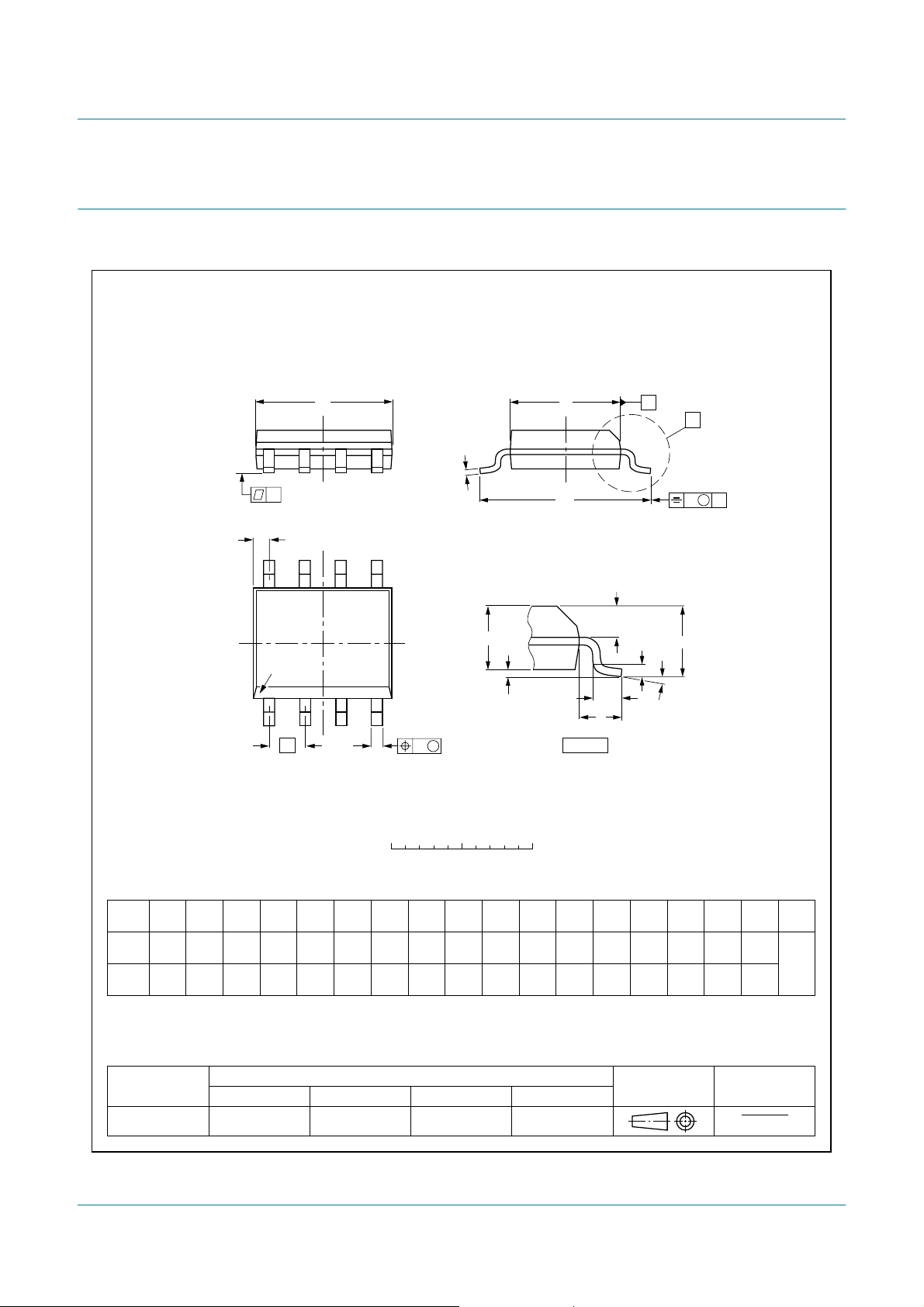
12. Package outline
PCA9517
Level translating I2C-bus repeater
SO8: plastic small outline package; 8 leads; body width 3.9 mm
D
c
y
Z
8
pin 1 index
1
e
5
A
2
A
4
w M
b
p
SOT96-1
E
H
E
1
detail X
A
X
v M
A
Q
(A )
L
p
L
A
3
θ
0 2.5 5 mm
scale
DIMENSIONS (inch dimensions are derived from the original mm dimensions)
mm
OUTLINE
VERSION
SOT96-1
A
A1A2A3b
max.
0.25
1.75
0.10
0.010
0.069
0.004
p
1.45
1.25
0.057
0.049
IEC JEDEC JEITA
076E03 MS-012
0.25
0.01
0.49
0.36
0.019
0.014
0.25
0.19
0.0100
0.0075
UNIT
inches
Notes
1. Plastic or metal protrusions of 0.15 mm (0.006 inch) maximum per side are not included.
2. Plastic or metal protrusions of 0.25 mm (0.01 inch) maximum per side are not included.
(1)E(2)
cD
5.0
4.8
0.20
0.19
REFERENCES
eHELLpQZywv θ
4.0
3.8
0.16
0.15
1.27
0.05
6.2
5.8
0.244
0.228
1.05
1.0
0.4
0.039
0.016
0.7
0.6
0.028
0.024
0.25 0.10.25
0.010.010.041 0.004
EUROPEAN
PROJECTION
(1)
0.7
0.3
0.028
0.012
ISSUE DATE
99-12-27
03-02-18
o
8
o
0
Fig 14. Package outline SOT96-1 (SO8)
PCA9517_3 © NXP B.V. 2007. All rights reserved.
Product data sheet Rev. 03 — 30 January 2007 12 of 19
Page 13

NXP Semiconductors
PCA9517
Level translating I2C-bus repeater
TSSOP8: plastic thin shrink small outline package; 8 leads; body width 3 mm
D
y
Z
8
pin 1 index
5
14
e
w M
b
p
c
A
2
A
1
E
H
E
L
detail X
SOT505-1
A
X
v M
A
(A3)
L
p
A
θ
2.5 5 mm0
scale
DIMENSIONS (mm are the original dimensions)
A
A
UNIT
max.
mm
1.1
Notes
1. Plastic or metal protrusions of 0.15 mm maximum per side are not included.
2. Plastic or metal protrusions of 0.25 mm maximum per side are not included.
OUTLINE
VERSION
SOT505-1
1
0.15
0.05
A2A3b
0.95
0.25
0.80
IEC JEDEC JEITA
p
0.45
0.25
ceD
0.28
0.15
REFERENCES
(1)E(2)
3.1
2.9
3.1
2.9
0.65
5.1
4.7
LH
E
L
0.7
0.4
p
wyv
0.1 0.10.10.94
EUROPEAN
PROJECTION
(1)
Z
0.70
0.35
ISSUE DATE
θ
6°
0°
99-04-09
03-02-18
Fig 15. Package outline SOT505-1 (TSSOP8)
PCA9517_3 © NXP B.V. 2007. All rights reserved.
Product data sheet Rev. 03 — 30 January 2007 13 of 19
Page 14

NXP Semiconductors
13. Soldering
This text provides a very brief insight into a complex technology. A more in-depth account
of soldering ICs can be found in Application Note
soldering description”
13.1 Introduction to soldering
Soldering is one of the most common methods through which packages are attached to
Printed Circuit Boards (PCBs), to form electrical circuits. The soldered joint provides both
the mechanical and the electrical connection. There is no single soldering method that is
ideal for all IC packages. Wave soldering is often preferred when through-hole and
Surface Mount Devices (SMDs) are mixed on one printed wiring board; however, it is not
suitable for fine pitch SMDs. Reflow soldering is ideal for the small pitches and high
densities that come with increased miniaturization.
13.2 Wave and reflow soldering
Wave soldering is a joining technology in which the joints are made bysolder coming from
a standing wave of liquid solder. The wave soldering process is suitable for the following:
PCA9517
Level translating I2C-bus repeater
AN10365 “Surface mount reflow
.
• Through-hole components
• Leaded or leadless SMDs, which are glued to the surface of the printed circuit board
Not all SMDs can be wave soldered. Packages with solder balls, and some leadless
packages which have solder lands underneath the body, cannot be wave soldered. Also,
leaded SMDs with leads having a pitch smaller than ~0.6 mm cannot be wave soldered,
due to an increased probability of bridging.
The reflow soldering process involves applying solder paste to a board, followed by
component placement and exposure to a temperature profile. Leaded packages,
packages with solder balls, and leadless packages are all reflow solderable.
Key characteristics in both wave and reflow soldering are:
• Board specifications, including the board finish, solder masks and vias
• Package footprints, including solder thieves and orientation
• The moisture sensitivity level of the packages
• Package placement
• Inspection and repair
• Lead-free soldering versus PbSn soldering
13.3 Wave soldering
Key characteristics in wave soldering are:
• Process issues, such as application of adhesive and flux, clinching of leads, board
transport, the solder wave parameters, and the time during which components are
exposed to the wave
• Solder bath specifications, including temperature and impurities
PCA9517_3 © NXP B.V. 2007. All rights reserved.
Product data sheet Rev. 03 — 30 January 2007 14 of 19
Page 15

NXP Semiconductors
13.4 Reflow soldering
Key characteristics in reflow soldering are:
• Lead-freeversusSnPb soldering; note that a lead-free reflowprocess usually leads to
• Solder paste printing issues including smearing, release, and adjusting the process
• Reflow temperature profile; this profile includes preheat, reflow (in which the board is
Table 6. SnPb eutectic process (from J-STD-020C)
Package thickness (mm) Package reflow temperature (°C)
< 2.5 235 220
≥ 2.5 220 220
PCA9517
Level translating I2C-bus repeater
higher minimum peak temperatures (see Figure 16) than a PbSn process, thus
reducing the process window
window for a mix of large and small components on one board
heated to the peak temperature) and cooling down. It is imperative that the peak
temperature is high enoughforthe solder to makereliablesolder joints (a solder paste
characteristic). In addition, the peak temperature must be low enough that the
packages and/or boards are not damaged. The peak temperature of the package
depends on package thickness and volume and is classified in accordance with
Table 6 and 7
Volume (mm3)
< 350 ≥ 350
Table 7. Lead-free process (from J-STD-020C)
Package thickness (mm) Package reflow temperature (°C)
Volume (mm3)
< 350 350 to 2000 > 2000
< 1.6 260 260 260
1.6 to 2.5 260 250 245
> 2.5 250 245 245
Moisture sensitivity precautions, as indicated on the packing, must be respected at all
times.
Studies have shown that small packages reach higher temperatures during reflow
soldering, see Figure 16.
PCA9517_3 © NXP B.V. 2007. All rights reserved.
Product data sheet Rev. 03 — 30 January 2007 15 of 19
Page 16

NXP Semiconductors
Fig 16. Temperature profiles for large and small components
maximum peak temperature
temperature
MSL: Moisture Sensitivity Level
= MSL limit, damage level
minimum peak temperature
= minimum soldering temperature
PCA9517
Level translating I2C-bus repeater
peak
temperature
time
001aac844
For further information on temperature profiles, refer to Application Note
“Surface mount reflow soldering description”
14. Abbreviations
Table 8. Abbreviations
Acronym Description
CDM Charged Device Model
CMOS Complementary Metal Oxide Silicon
ESD ElectroStatic Discharge
HBM Human Body Model
2
C-bus Inter Integrated Circuit bus
I
MM Machine Model
SMBus System Management Bus
AN10365
.
PCA9517_3 © NXP B.V. 2007. All rights reserved.
Product data sheet Rev. 03 — 30 January 2007 16 of 19
Page 17

NXP Semiconductors
PCA9517
Level translating I2C-bus repeater
15. Revision history
Table 9. Revision history
Document ID Release date Data sheet status Change notice Supersedes
PCA9517_3 20070130 Product data sheet - PCA9517_2
Modifications:
PCA9517_2
(9397 750 14918)
PCA9517_1
(9397 750 13252)
• The format of this data sheet has been redesigned to comply with the new identity guidelines of
NXP Semiconductors.
• Legal texts have been adapted to the new company name where appropriate.
• Section2“Features”,15thbulletitem:changed“200 V MM per JESD22-A115” to “150 V MM per
JESD22-A115”
• Table 4 “Static characteristics” added new Table note 3, and its reference in sub-section “Input
and output SDAA and SCLA”, symbol V
.
IL
• added (new) Figure 7 “Typical application of PCA9517 driving a short cable”
• Figure 8 “Bus A (0.9 V to 5.5 V bus) waveform”: SDA signal modified
• Figure 9 “Bus B (2.7 V to 5.5 V) waveform”: SDA signal modified
• Table 5 “Dynamic characteristics”:
, A-side: changed reference to timing diagram from Figure 11 to Figure 10
– t
t(LH)
, A-side: changed reference to timing diagram from Figure 11 to Figure 10
– t
t(HL)
, B-side: changed reference to timing diagram from Figure 10 to Figure 11
– t
t(LH)
, B-side: changed reference to timing diagram from Figure 10 to Figure 11
– t
t(HL)
20060615 Product data sheet - PCA9517_1
20041005 Product data sheet - -
PCA9517_3 © NXP B.V. 2007. All rights reserved.
Product data sheet Rev. 03 — 30 January 2007 17 of 19
Page 18

NXP Semiconductors
16. Legal information
16.1 Data sheet status
PCA9517
Level translating I2C-bus repeater
Document status
Objective [short] data sheet Development This document contains data from the objective specification for product development.
Preliminary [short] data sheet Qualification This document contains data from the preliminary specification.
Product [short] data sheet Production This document contains the product specification.
[1] Please consult the most recently issued document before initiating or completing a design.
[2] The term ‘short data sheet’ is explained in section “Definitions”.
[3] The productstatus of device(s) described in this documentmay have changedsince this document was published and may differ in case of multiple devices. Thelatest productstatus
information is available on the Internet at URL
[1][2]
Product status
16.2 Definitions
Draft — The document is a draft version only. The content is still under
internal review and subject to formal approval, which may result in
modifications or additions. NXP Semiconductors does not give any
representations or warranties as to the accuracy or completeness of
information includedherein and shallhave noliability for theconsequences of
use of such information.
Short data sheet — A short data sheet is an extract from a full data sheet
with thesame product typenumber(s) and title.A short datasheet is intended
for quickreference only andshould not be reliedupon to contain detailedand
full information. For detailed and full information see the relevant full data
sheet, which is available on request via the local NXP Semiconductors sales
office. In case of any inconsistency or conflict with the short data sheet, the
full data sheet shall prevail.
16.3 Disclaimers
General — Information in this document is believed to be accurate and
reliable. However,NXP Semiconductors does notgive any representationsor
warranties, expressed or implied,as to the accuracyor completeness ofsuch
information and shall have no liability for the consequences of use of such
information.
Right to make changes — NXP Semiconductors reservesthe right to make
changes to information published in this document, including without
limitation specifications and product descriptions, at any time and without
notice. Thisdocument supersedes and replaces allinformation supplied prior
to the publication hereof.
Suitability for use — NXP Semiconductors products are not designed,
authorized or warranted to be suitable for use in medical, military, aircraft,
space or life support equipment, nor in applications where failure or
malfunction ofa NXP Semiconductorsproduct canreasonably be expected to
[3]
http://www.nxp.com.
Definition
result in personal injury, death or severe property or environmental damage.
NXP Semiconductors accepts no liability for inclusion and/or use of NXP
Semiconductors products in such equipment or applications and therefore
such inclusion and/or use is at the customer’s own risk.
Applications — Applications that are described herein for any of these
products are for illustrative purposes only. NXP Semiconductors makes no
representation or warranty that such applications will be suitable for the
specified use without further testing or modification.
Limiting values — Stress above one or more limiting values (as defined in
the AbsoluteMaximum Ratings System ofIEC 60134) may causepermanent
damage tothe device. Limitingvalues are stressratings only andoperation of
the device at these or any other conditions above those given in the
Characteristics sections of this document is not implied. Exposure to limiting
values for extended periods may affect device reliability.
Terms and conditions of sale — NXP Semiconductors products are sold
subject to the generalterms and conditions ofcommercial sale, as published
at
http://www.nxp.com/profile/terms, including those pertaining to warranty,
intellectual property rights infringement and limitation of liability, unless
explicitly otherwise agreed to in writing by NXP Semiconductors. In case of
any inconsistency or conflict between information in this document and such
terms and conditions, the latter will prevail.
No offer to sell or license — Nothing in this document may be interpreted
or construed as an offer to sell products that is open for acceptance or the
grant, conveyance orimplicationof any license underany copyrights, patents
or other industrial or intellectual property rights.
16.4 Trademarks
Notice: Allreferenced brands,product names,service namesand trademarks
are the property of their respective owners.
I2C-bus — logo is a trademark of NXP B.V.
17. Contact information
For additional information, please visit: http://www.nxp.com
For sales office addresses, send an email to: salesaddresses@nxp.com
PCA9517_3 © NXP B.V. 2007. All rights reserved.
Product data sheet Rev. 03 — 30 January 2007 18 of 19
Page 19

NXP Semiconductors
18. Contents
1 General description. . . . . . . . . . . . . . . . . . . . . . 1
2 Features . . . . . . . . . . . . . . . . . . . . . . . . . . . . . . . 1
3 Ordering information. . . . . . . . . . . . . . . . . . . . . 2
4 Functional diagram . . . . . . . . . . . . . . . . . . . . . . 2
5 Pinning information. . . . . . . . . . . . . . . . . . . . . . 3
5.1 Pinning . . . . . . . . . . . . . . . . . . . . . . . . . . . . . . . 3
5.2 Pin description . . . . . . . . . . . . . . . . . . . . . . . . . 3
6 Functional description . . . . . . . . . . . . . . . . . . . 3
6.1 Enable. . . . . . . . . . . . . . . . . . . . . . . . . . . . . . . . 4
6.2 I
7 Application design-in information . . . . . . . . . . 5
8 Limiting values. . . . . . . . . . . . . . . . . . . . . . . . . . 8
9 Static characteristics. . . . . . . . . . . . . . . . . . . . . 9
10 Dynamic characteristics . . . . . . . . . . . . . . . . . 10
10.1 AC waveforms. . . . . . . . . . . . . . . . . . . . . . . . . 11
11 Test information. . . . . . . . . . . . . . . . . . . . . . . . 11
12 Package outline . . . . . . . . . . . . . . . . . . . . . . . . 12
13 Soldering . . . . . . . . . . . . . . . . . . . . . . . . . . . . . 14
13.1 Introduction to soldering . . . . . . . . . . . . . . . . . 14
13.2 Wave and reflow soldering . . . . . . . . . . . . . . . 14
13.3 Wave soldering. . . . . . . . . . . . . . . . . . . . . . . . 14
13.4 Reflow soldering . . . . . . . . . . . . . . . . . . . . . . . 15
14 Abbreviations. . . . . . . . . . . . . . . . . . . . . . . . . . 16
15 Revision history. . . . . . . . . . . . . . . . . . . . . . . . 17
16 Legal information. . . . . . . . . . . . . . . . . . . . . . . 18
16.1 Data sheet status . . . . . . . . . . . . . . . . . . . . . . 18
16.2 Definitions. . . . . . . . . . . . . . . . . . . . . . . . . . . . 18
16.3 Disclaimers . . . . . . . . . . . . . . . . . . . . . . . . . . . 18
16.4 Trademarks. . . . . . . . . . . . . . . . . . . . . . . . . . . 18
17 Contact information. . . . . . . . . . . . . . . . . . . . . 18
18 Contents . . . . . . . . . . . . . . . . . . . . . . . . . . . . . . 19
2
C-bus systems . . . . . . . . . . . . . . . . . . . . . . . . 4
PCA9517
Level translating I2C-bus repeater
Please be aware that important notices concerning this document and the product(s)
described herein, have been included in section ‘Legal information’.
© NXP B.V. 2007. All rights reserved.
For more information, please visit: http://www.nxp.com
For sales office addresses, please send an email to: salesaddresses@nxp.com
Date of release: 30 January 2007
Document identifier: PCA9517_3
 Loading...