

Page 1

PCA9420
Power management IC for low-power microcontroller
applications
Rev. 2 — 26 January 2021 Product data sheet
1 General description
The PCA9420 is a highly-integrated Power Management IC (PMIC), targeted to provide
a full power management solution for low power microcontroller applications or other
similar applications.
The device consists of a linear battery charger capable of charging up to 315 mA current.
It has an I2C programmable Constant Current (CC) and Constant Voltage (CV) values
for flexible configuration. Various built-in protection features such as input overvoltage
protection, overcurrent protection, thermal protection, etc. are also provided for safe
battery charging. It also features JEITA compliant charging.
The device also integrates two step-down (buck) DC/DC converters which have I2C
programmable output voltage. Both buck regulators have integrated high-side and lowside switches and related control circuitry, to minimize the external component counts;
a Pulse-Frequency Modulation (PFM) approach is utilized to achieve better efficiency
under light load condition. Other protection features such as overcurrent protection,
under-voltage lockout (UVLO), etc. are also provided. By default, the input for these
regulators is powered by either VIN or VBAT, whichever is greater.
In addition, two on-chip LDO regulators are provided to power up various voltage rails in
the system.
Other features such as FM+ I2C-bus interface, chip enable, interrupt signal, etc. are also
provided.
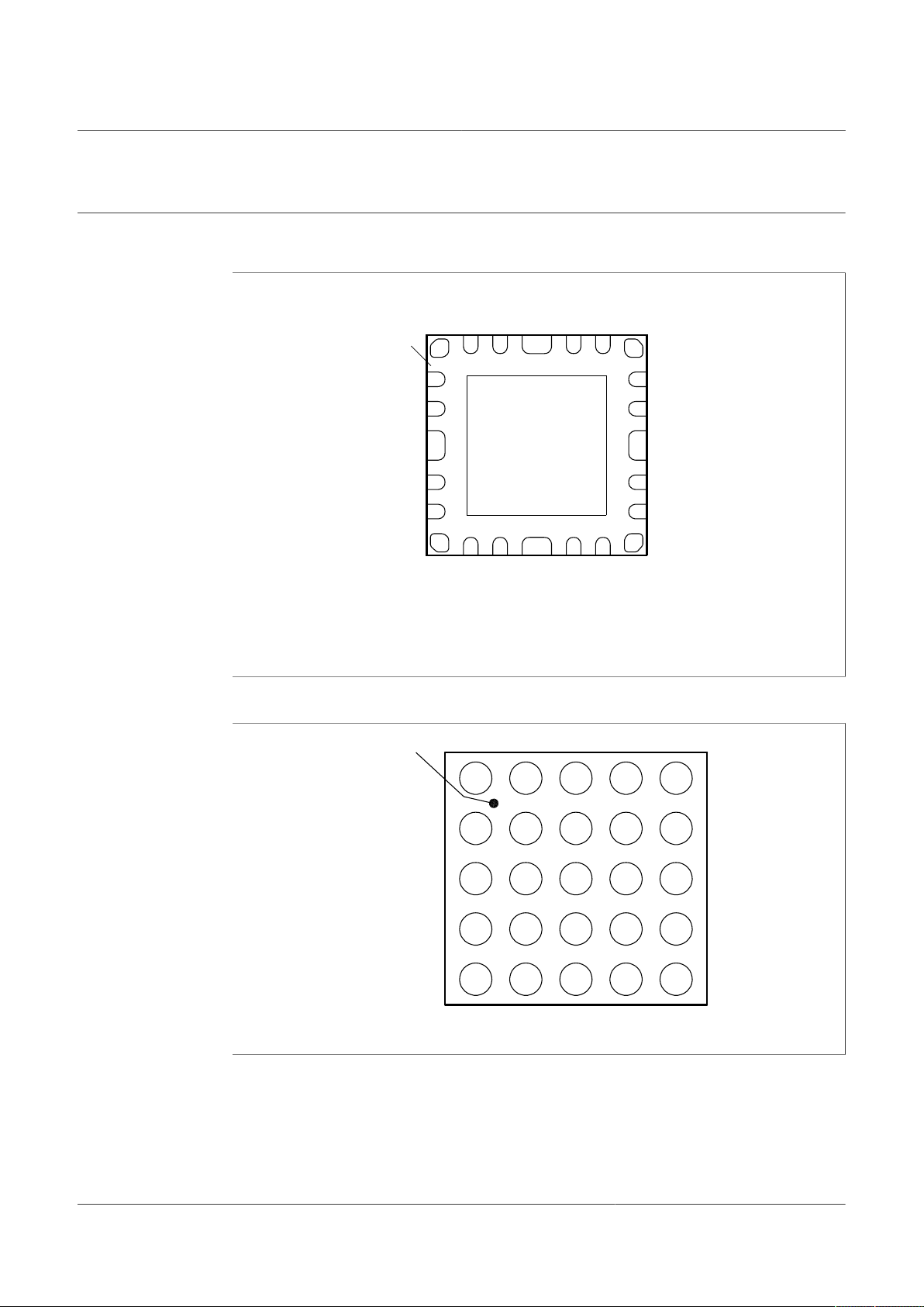
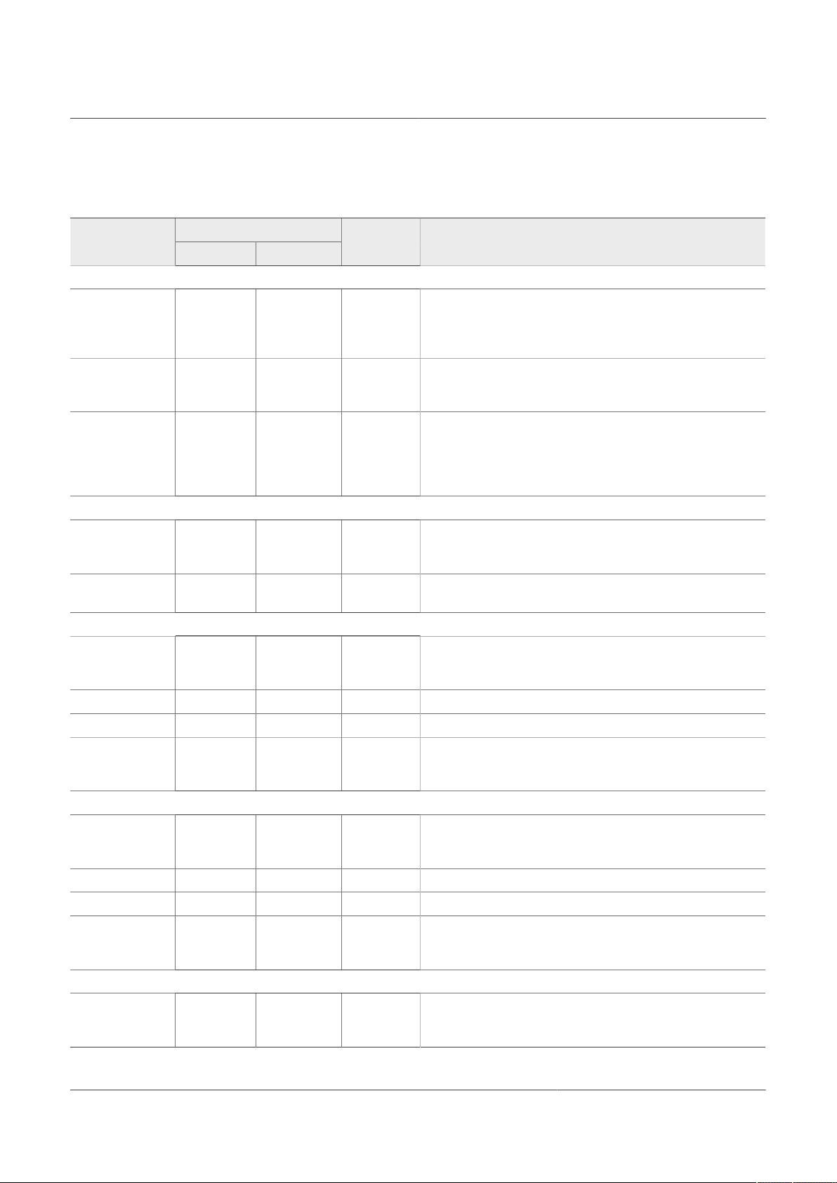
The chip is offered in 2.09 mm x 2.09 mm, 5 x 5 bump, 0.4 mm pitch WLCSP package;
and 3 mm x 3 mm, 24-pin QFN package.
2 Features and Benefits
• Linear battery charger for charging single cell li-ion battery
– 20 V tolerance on VIN pin
– Programmable input OVP (5.5 V or 6 V)
– Programmable constant current (up to 315 mA) and pre-charge low voltage current
threshold
– Programmable constant voltage regulation
– Programmable automatic recharge voltage and termination current threshold
– Built-in protection features such as input OVP, battery SCP, thermal protection
– JEITA compliant
– Battery attached detection
– Over-temperature protection
Page 2

NXP Semiconductors
• Two step-down DC/DC converters
– Very low quiescent current
– Programmable output voltage
– SW1: core buck converter, 0.5 V~1.5 V output, 25 mV/step, and a fixed 1.8 V, up to
– SW2: system buck converter, 1.5 V~2.1 V/2.7 V~3.3 V output, 25 mV/step, up to
– Low power mode for extra power saving
• Two LDOs
– Programmable output voltage regulation
– LDO1: always-on LDO, 1.70 V~1.90 V output, 25 mV/step, up to 1 mA
– LDO2: system LDO, 1.5 V~2.1 V/2.7 V~3.3 V output, 25 mV/step, up to 250 mA
• 1 MHz I2C-bus slave interface
• -40 °C ~ +85 °C ambient temperature range
• Offered in 5 x 5 bump-array WLCSP and 24-pin QFN package
3 Applications
PCA9420
Power management IC for low-power microcontroller applications
250 mA
500 mA
• Low power microcontroller application
4 Ordering information
Table 1. Ordering information
PackageType number Topside
marking
PCA9420BS 420 HVQFN24 plastic thermal enhanced very thin quad flat package; no
PCA9420UK 9420 WLCSP25 wafer level chip-scale package, 25 terminals, 0.4 mm
4.1 Ordering options
Table 2. Ordering options
Type number Orderable part
number
PCA9420BS PCA9420BSAZ HVQFN24 REEL 7" Q2 NDP 1400 -40°C to +85°C
PCA9420UK PCA9420UKZ WLCSP25 REEL 7" Q1 DP CHIPS 3000 -40°C to +85°C
Name Description Version
SOT905-1
leads; 24 terminals; body 3 x 3 x 0.85 mm
SOT1401-4
pitch, 2.09 mm x 2.09 mm x 0.525 mm body
Package Packing method Minimum order
quantity
Temperature range
PCA9420 All information provided in this document is subject to legal disclaimers. © NXP B.V. 2021. All rights reserved.
Product data sheet Rev. 2 — 26 January 2021
2 / 82
Page 3

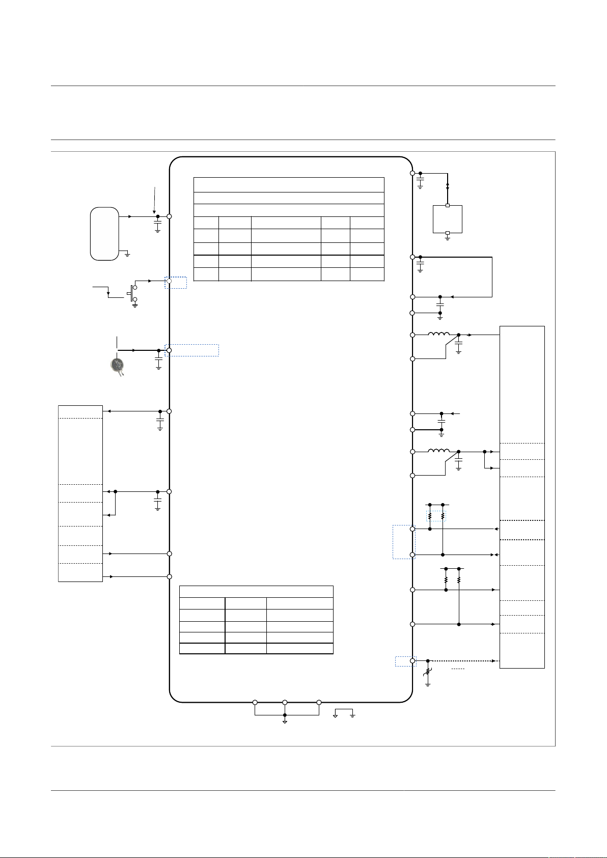
NXP Semiconductors
aaa-033067
Max 315mA
Linear Charger
O
VP
Detection
(5.5V default or
6V over I2C
)
PCA9420
Main
Contro
l
Blo
cks
VIN
ASY
S
VBA
T
1-Cel
l
Li-Io
n
Battery
+ (VBAT
)
- (GND)
STEP-DOWN
CONVERTER 1
250mA
(0.5V-1.5V
in 25mV steps
& fixed 1.8V)
STEP-DOWN
CONVERTER 2
500mA
(1.5V-2.1V in
25mV steps
)
(or 2.7V-3.3V
in 25mV steps
)
PSYS1
E
N
4.7
µF/
1
0V
PGND1
LX1
ASY
S
2.2µH
SW1_OU
T
50Ω
PSYS2
PGND2
LX2
2.2µH
SW2_OU
T
E
N
I
2
C
I2C
1µF/
1
0V
50Ω
VDDCORE
RT600
LDO
1
1
mA
(1.7V-1.9V
in 25mV steps
)
LDO
2
250mA
(1.5V-2.1V in
25mV steps)
(or 2.7V-3.3V
in 25mV steps
)
LDO1_OUT
50Ω
LDO2_OUT
50Ω
I
N
ASY
S
VBA
T_BKU
P
I
N
ASY
S
VIN
_
UVLO
T
herma
l
shutdow
n
O
FF
O
N
Debounc
e
Filter
(200µs)
On-Ke
y
1MΩ
+
-
2.5V
or VBAT
Long-Key
Debounce
Filter
(4s, 8s(default
)
,12s,16s
)
2.2µF/
10V
2.9V,3.1V(default)
,
3.3V,3.5
V
200m
V
ASYS_
Pre
-
warning
+
-
3.3V,3.4V
,
3.5V (default),3.6
V
100m
V
ASYS_
UVL
O
+
-
100mV
AGND1AGND
2
1µF/
1
0V
10µF/
6.3
V
2.2µF/
1
0V
10µF/
6.3
V
VBA
T
0.47µF
/
6.3
V
Coin
battery
O
N
Power-o
n
from off o
r
ship-mod
e
2.4V,2.5V, 2.6V,
2.7V (default
)
Recycle
Power rail
s
VBAT
_
BKUP_
UVLO
+
-
1.9
V
100m
V
Watchdog
(disable, 16s,
32s, 64s)
SCL
SDA
TS
N
TC
N
TC
C
ontrol
Block
Up to 1MHz
I2C Interface
VDD_AO1V8
Optio
n
ADC
MOD
E
SELECTION
MODESEL0
MODESEL1
AGND3
1µF/
6.3
V
2.2µF
/
6.3
V
Power-Good
&
Rese
t
SYSRS
Tn
Interrupts
INTB
R
1
R1=R2=20kΩ to 220kΩ
R
2
PMIC_IRQN
(VDD_AO1V8)
+
-
20°
C
T
DIE
Thermal
Regulatio
n
(80°C t
o
115°C
)
ASY
S
3-bit
programmable
(95°
C to 125°C
in 5°
C steps)
T
herma
l
warni
ng
+
-
20°
C
T
DIE
2-bit
programmabl
e
(75°C to 90°C
in 5°C steps)
50µA 5
µA
25-Bump WLCSP, 0.4mm pitch,
2.09mm x 2.09mm
ASY
S
E
N
I
2
C
E
N
I2C
E
N
I2C
SHI
P
MOD
E
ENTE
R
O
R
SHIP_EN_x=1
EXI
T
Valid VIN
Valid VIN
SHIP_WKUP_CFG=
0
Battery
absence
detection
E
N
I2C
1
2
A programme
d
I
CHG_CC
X
Power-down
sequence
PWR_DN_EN=
1
β selction
3-bit programmabl
e
From 3434k to 4750
k
Add 1.2V
offset
I
2
C
Add 1.2
V
offse
t
Default:1.
0V
Default:1.
8V
VDDIO_1,2,3,
and/or
4
Always-on
1.8V
Default:
3.3
V
Reverse
Blocking
Note: All directions for the arrows in the schematic are
made from the PCA9420 perspective.
Short on PCB
i.MXRT
*
RT60
0
i.MXRT
*
VDD1V8 and
other 1.8V powe
r
PMIC_I2C_SC
L
(VDDIO_1)
PMIC_I2C_SD
A
(VDDIO_1)
VDD_AO1V8
VDDIO_1,2,3,
and/or
4
USB1_VDD3V3
and other
3V powe
r
RESETN
(VDD_AO1V8)
PMIC_MODE0
(VDD_AO1V8)
PMIC_MODE1
(VDD_AO1V8)
Option: can be remove if an
internal pull-up R is availabl
e
on i.MXRT* device
VDDIO_1
MODESEL
1
MODESEL0
EN_MODE_SEL_BY_PIN_x=
1
Output Voltage Settin
g
LOW (0)
HIGH (1)
LOW (0)
LOW (0)
HIGH (1)LOW (0)
HIGH (1)HIGH (1
)
Mode Setting
0
Mode Setting
1
Mode Setting
2
Mode Setting
3
(x can be 0, 1, 2 or 3)
Can be connected to any AD
C
Regulator
Default (V)*Output Range
BUCK1
1.0
(MTP
)
0.5V to 1.5V and fixed 1.8
V
BUCK2
LDO1
LDO2
1.5V to 2.1V or 2.7V to 3.
3V
* : Regardless of mode setting
1.7V to 1.9V
1.5V to 2.1V or 2.7V to 3.
3V
Resolution
25mV
Max Curren
t
250mA
25mV
25mV
25mV
500mA
1m
A
250mA
Linear charger: 0mA to 315mA in 5mA steps for charge curre
nt
Input Current Limit (typical): 85mA, 255mA, 425mA, 595mA, 765mA, 935mA,
1105mA, or disable
1.8
(MTP
)
1.8
(MTP
)
3.3
(MTP
)
If VIN is greater than 6V, the
voltage rating on the capacitor of
2.2µF/10V shall be changed to a
higher voltage than a maximum
voltage in applications.
VIN ≤ 6V
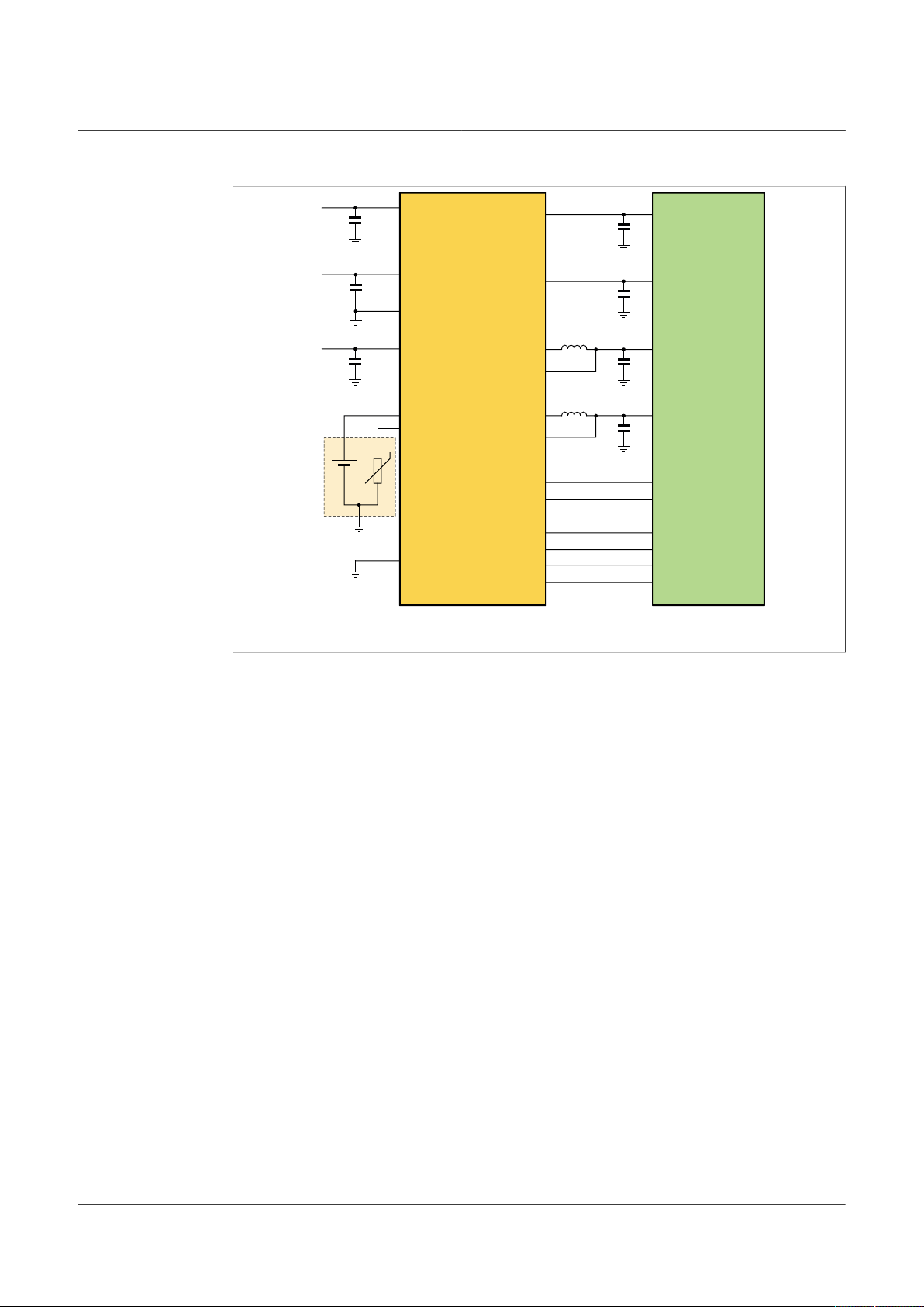
5 Simplified block diagram
PCA9420
Power management IC for low-power microcontroller applications
PCA9420 All information provided in this document is subject to legal disclaimers. © NXP B.V. 2021. All rights reserved.
Product data sheet Rev. 2 — 26 January 2021
Figure 1. Simplified block diagram
3 / 82
Page 4
NXP Semiconductors
aaa-033076
17
Transparent top view
Exposed pad
2
4
P
G
N
D
2
232
2
201
9
1
8
V
B
A
T
2
1
terminal 1
index area
PCA9420BS
15
14
13
16
3
1
4
5
2
SDA 6
7
8
10
11
LDO1_OUT 12
9
SCL
ON
SW2_OUT
PSYS2
LX2
SYSRSTn
INTB
AGND1
MODESEL1
MODESEL0
VBAT_BKUP
TS
LDO2_OUT
VIN
ASYS
S
W
1
_
O
U
T
P
S
Y
S
1
A
G
N
D
2
LX
1
P
G
N
D
1
aaa-033077
A
SW2_
O
UT
AGND
2
AGN
D
1
T
S
INT
B
SYS
RSTn
B
C
1
2
3
4
VBAT_
BKUP
ASYS
O
N
LDO
2
_OU
T
VI
N
SW1_
O
UT
PS
YS
2
LX2
5
S
CL
PGND
1
LX1
VBA
T
PSYS
1
PGND
2
D
MODE
SEL
1
AGND
3
LDO
1
_OU
T
E
pin A1
index area
MOD
E
SEL0
S
DA
6 Pinning information
6.1 Pinning
PCA9420
Power management IC for low-power microcontroller applications
Figure 2. PCA9420BS pinout (HVQFN24) – top view
Figure 3. PCA9420UK pinout (WLCSP25) – top view
PCA9420 All information provided in this document is subject to legal disclaimers. © NXP B.V. 2021. All rights reserved.
Product data sheet Rev. 2 — 26 January 2021
4 / 82
Page 5
NXP Semiconductors
PCA9420
Power management IC for low-power microcontroller applications
6.2 Pin description
Table 3. Pin Description
PinSymbol
HVQFN24 WLCSP25
INPUT SUPPLY
VIN 16 C1 P Input supply voltage. Bypass with a 2.2µF/10V ceramic
ASYS 17 B1 P Bypass output of VIN and input supply voltage for LDO2,
VBAT_BKUP 13 D2 P Backup battery input voltage. LDO1 is powered by the
LINEAR CHARGER
VBAT 18 A1 P Battery (+) connection point. A typical 1µF/10V decoupling
TS 14 C2 I Battery temperature sensing pin. An external thermistor is
BUCK1 STEP_DOWN CONVERTER (SW1)
PSYS1 20 A2 P Input supply for SW1. Bypass with a typical 1µF/10V
LX1 22 A3 P Switching node for SW1. Connect to a 2.2µH inductor.
SW1_OUT 19 B2 I Feedback pin. Bypass with a 10µF/6.3V ceramic capacitor.
PGND1 23 A4 P Power ground for buck 1 (SW1). Connect ground nodes of
BUCK2 STEP_DOWN CONVERTER (SW2)
PSYS2 2 C5 P Input supply for SW2. Bypass with a typical 2.2µF/10V
LX2 1 B5 P Switching node for SW2. Connect to a 2.2µH inductor.
SW2_OUT 3 B4 I Feedback pin. Bypass with a 10µF/6.3V ceramic capacitor.
PGND2 24 A5 P Power ground for buck 2 (SW2). Connect ground nodes of
LOW_DROPOUT REGULATORS (LDO1 and LDO2)
LDO1_OUT 12 E1 P LDO1 output. It is always-ON supply. The input supply is a
Pin Type Description
capacitor. If VIN is greater than 6V, the voltage rating shall
be changed to a higher voltage than the maximum voltage
in applications.
connect with a typical 4.7µF or 10µF/10V decoupling
capacitor.
greater of ASYS or VAT_BKUP. If a back-up battery with a
coin cell is not connected, connect the pin to VBAT power
domain. Connect with a typical 0.47µF/6.3V decoupling
capacitor.
capacitor should be connected between VBAT to system
ground.
connected between TS pin and system ground.
ceramic capacitor. Connect to ASYS power domain as short
as possible in the system.
two bypass capacitors for PSYS1 and SW1_OUT as close
to PGND1 pin as possible in the system.
ceramic capacitor. Connect to ASYS power domain as short
as possible in the system.
two bypass capacitors for PSYS2 and SW2_OUT as close
to PGND2 pin as possible in the system.
higher voltage between ASYS and VBAT_BKUP. Bypass
with a 1µF/6.3V ceramic capacitor.
PCA9420 All information provided in this document is subject to legal disclaimers. © NXP B.V. 2021. All rights reserved.
Product data sheet Rev. 2 — 26 January 2021
5 / 82
Page 6
NXP Semiconductors
PCA9420
Power management IC for low-power microcontroller applications
Table 3. Pin Description...continued
PinSymbol
HVQFN24 WLCSP25
LDO2_OUT 15 D1 P LDO2 output. The input supply is ASYS. Bypass with a
LOGIC INPUTS
ON 4 C4 I
MODESEL0 7 E4 I Mode selection input pin #1
MODESEL1 8 E3 I Mode selection input pin #2
LOGIC OUTPUTS
INTB 10 D4 O
SYSRSTn 11 D3 O
SERIAL I2C INTERFACE
SCL 5 D5 I
SDA 6 E5 I/O
DEVICE GROUND
AGND1 9 B3 P
AGND2 21 C3 P
AGND3 E2 P
Exposed
Pad
Pin Type Description
2.2µF/6.3V ceramic capacitor.
ON Pin with an internal pull-up resistor, 1MΩ typ, to either
2.5V or VBAT. Refer to Section 8.3 for more details.
Interrupt output, Open-drain type. Place a pull-up resistor
from 20kΩ to 220kΩ to a system I/O supply rail.
Reset output for external MCU, Open-drain type. Place a
pull-up resistor from 20kΩ to 220kΩ to a system I/O supply
rail.
I2C Interface clock pin. Place a pull-up resistor between
2.2kΩ and 10kΩ to a system I/O supply rail.
I2C Interface data pin. Place a pull-up resistor between
2.2kΩ and 10kΩ to a system I/O supply rail.
Analog ground. It shall be connected to system ground
through a via. Do not connect AGND1 and AGND2 to
PGND1 or PGND2 on the top PCB layer in the system.
Exposed pad. Connect to system ground
P = Power, I = Input, I/O = input/output
PCA9420 All information provided in this document is subject to legal disclaimers. © NXP B.V. 2021. All rights reserved.
Product data sheet Rev. 2 — 26 January 2021
6 / 82
Page 7
NXP Semiconductors
aaa-033078
PCA9420
VIN
ASYS
VBAT
1-Cell
Li-Ion
Battery
+ (VBAT)
- (GND)
PSYS1
4.7µF/
10V
PGND1
LX1
2.2µH
SW1_OUT
PSYS2
PGND2
LX2
2.2µH
SW2_OUT
1µF/
10V
VDDCORE
LDO1_OUT
LDO2_OUT
VBAT_BKUP
OFF
ON
On-Key
button
2.2µF/
10V
AGND1 AGND2
1µF/
10V
10µF/
6.3V
2.2µF/
10V
10µF/
6.3V
VBAT
0.47µF/
6.3V
Coin
battery
ON
SCL
SDA
TS
NTC
VDD_AO1V8
Option
ADC
MODESEL0
MODESEL1
AGND3
1µF/
6.3V
2.2µF/
6.3V
SYSRSTn
INTB
R1
R1=R2=100-220kΩ
R2
PMIC_IRQN
(VDD_AO1V8)
25-Bump WLCSP, 0.4m m pi tch,
2.1mm x 2. 1mm
ASYS
Default:1.0V
Default:1.8V
VDDIO_1,2,3,
and/or 4
Always-on
1.8V
Default:
3.3V
Note: All dir ections f or t he arrows in the
schematic are made from the PCA9420
perspecti ve.
Short on PCB
i.MXRT
RT5xx
RT6xx
VDD1V8 and
other 1.8V power
PMIC_I2C_SCL
(VDDIO_1)
PMIC_I2C _SDA
(VDDIO_1)
VDD_AO1V8
VDDIO_1,2,3,
and/or 4
USB1_VDD3V3
and other
3V.3V power
RESETN
(VDD_AO1V8)
PMIC_MO DE0
(VDD_AO1V8)
PMIC_MO DE1
(VDD_AO1V8)
Option: can be removed if an
internal pull-up R is available
on i.MXRT* device
VDDIO_1
Input Supply
VBUS
GND
C1
C4
D2
E1
D1
E4
E3
B3 C3 E2
C2
D3
D4
E5
D5
B4
B5
A5
C5
B2
A3
A4
A2
B1
A1
If a coil cell is not used, tie
with the VBAT power domain
If the pin is not used,
leave the pin open
If the pin is not used,
leave the pin open
If the pin is not used,
leave the pin open
MODESEL1
MODESEL0
EN_MODE_SEL_BY_PIN_x=1
Output Voltage Setting
LOW (0)
HIGH (1)
LOW (0)
LOW (0)
HIGH (1) LOW (0)
HIGH (1) HIGH (1)
Mode Setting 0
Mode Setting 1
Mode Setting 2
Mode Setting 3
(x can be 0, 1, 2 or 3)
MODESEL1
MODESEL0
EN_MODE_SEL_BY_PIN_x=1
Output Voltage Setting
LOW (0)
HIGH (1)
LOW (0)
LOW (0)
HIGH (1) LOW (0)
HIGH (1) HIGH (1)
Mode Setting 0
Mode Setting 1
Mode Setting 2
Mode Setting 3
(x can be 0, 1, 2 or 3)
Can be connected to any ADC
Regulator
Default (V)
*
Output Range
BUCK1
1.0
(MTP)
0.5V to 1.5V and fixed 1.8V
BUCK2
LDO1
LDO2
1.5V to 2.1V or 2.7V to 3.3V
* : Regardless of mode setting
1.7V to 1.9V
1.5V to 2.1V or 2.7V to 3.3V
Resolution
25mV
Max Current
250mA
25mV
25mV
25mV
500mA
1mA
250mA
Linear charger: 0mA to 315mA in 5mA steps for charge current
Input Current Limit (typical): 85mA, 255mA, 425mA, 595mA, 765mA, 935mA,
1105mA, or disable
1.8
(MTP)
1.8
(MTP)
3.3
(MTP)
Regulator
Default (V)
*
Output Range
BUCK1
1.0
(MTP)
0.5V to 1.5V and fixed 1.8V
BUCK2
LDO1
LDO2
1.5V to 2.1V or 2.7V to 3.3V
* : Regardless of mode setting
1.7V to 1.9V
1.5V to 2.1V or 2.7V to 3.3V
Resolution
25mV
Max Current
250mA
25mV
25mV
25mV
500mA
1mA
250mA
Linear charger: 0mA to 315mA in 5mA steps for charge current
1.8
(MTP)
1.8
(MTP)
3.3
(MTP)
VIN ≤ 6V
If VIN is greater than 6V, the voltage
rating on the capacitor of 2.2µF/10V
shall be changed to a higher
voltage than a maximum voltage
in applications.
i.MXRT
RT5xx
RT6xx
7 System configuration diagram
Power management IC for low-power microcontroller applications
PCA9420
Figure 4. System configuration diagram; i.MXRT series
PCA9420 All information provided in this document is subject to legal disclaimers. © NXP B.V. 2021. All rights reserved.
Product data sheet Rev. 2 — 26 January 2021
7 / 82
Page 8
NXP Semiconductors
aaa-033079
PCA9420
K4 Family MC
U
LDO
2_OUT
(Syst
em LDO)
LDO
1_OUT
(
AO_LDO)
SW1_OUT
(
Cor
e Buck)
LX1
SW2_OUT
(SY
S Buck)
LX2
SYSRSTn
M
ODESEL0
M
ODESEL1
ON
SCL
SDA
INTB
V
IN
ASYS
PSYS1
PSYS2
VBAT_
BKU
P
Battery
Pac
k
VBAT
T
S
PGND
AGND1/2
/3
LPI2Cn_S
CL
LPI2Cn_SD
A
GPIO_n
RESET_n
VDD_BA
T
VDD_IO
SPM_LPREQ
VDD_COR
E
VDD_SY
S
RTC_WAKEUP_n
T
PCA9420
Power management IC for low-power microcontroller applications
Figure 5. System configuration diagram; K4-family MCU
PCA9420 All information provided in this document is subject to legal disclaimers. © NXP B.V. 2021. All rights reserved.
Product data sheet Rev. 2 — 26 January 2021
8 / 82
Page 9

NXP Semiconductors
8 Functional description
8.1 ASYS
The ASYS pin serves as the input power pin for SW1, SW2 and LDO2. Internally by
default it’s powered by either VIN or VBAT, whichever is greater. The internal ASYS input
selection circuit ensures a seamless transition when its input source changes from VIN to
VBAT, or vice versa.
Through I2C register setting selection (SYS_INPUT_SEL [1:0]), the user also has the
option to choose the ASYS input source. However, upon power cycling and/or chip reset,
the ASYS input source goes back to the default setting (option 1 below).
SYS_INPUT_SEL [1:0]
1. 2b’00: From either VBAT or VIN, whichever is greater (default setting);
2. 2b’01: From VBAT only;
3. 2b’10: From VIN only;
4. 2b’11: Disconnect from VBAT or VIN (not a normal operation condition, for test
purposes only).
PCA9420
Power management IC for low-power microcontroller applications
An I2C programmable pre-warning ASYS voltage threshold (ASYS_PRE_WARNING
[1:0]) can also be used to indicate when ASYS voltage drops below the ASYS prewarning threshold voltage, which triggers an interrupt event.
If any peripheral regulators are connected to ASYS node, the ASYS node follows a VIN
voltage up to a programmed OVP threshold (either 5.5V or 6V) with a various voltage
difference depending on a load current.
8.2 VBAT_BKUP (back-up battery input)
Internally, the input power source for LDO1 is provided by either VBAT_BKUP or ASYS,
whichever is greater. When a coin cell battery (or similar battery) is used in the system
as a backup battery, it can be connected to VBAT_BKUP; thus the LDO1 is powered
by either ASYS or the backup battery. When no such backup battery is used, the
VBAT_BKUP pin should always be connected to VBAT.
8.3 ON
The ON pin has the following functions implemented:
1. ON pin has internal 1MΩ pull-up resistor to either 2.5V or VBAT depending on VBAT
voltage. If VBAT is less than 3V, ON is pulled up to 2.5V and if VBAT is greater than
3V, it is pulled to VBAT.
Falling edge (filtered after deglitching time, 200µs typ), active-low signal enables the
chip. If the chip stays in ship mode before applying ON falling edge, upon the filtered
falling edge of the ON pin, the chip exits ship mode to start up into Mode Setting 0.
If the device is already in the middle of power-up or power-down sequence, the falling
edge applied on the ON pin is ignored by the chip.
1. Long press (duration time, 4s, 8s, 12s or 16s, is programmable via I2C,
ON_GLT_LONG [1:0]). If the logic low signal is applied continuously over a
programmed duration, the chip gets reset and recycles all power rails to their default
values
PCA9420 All information provided in this document is subject to legal disclaimers. © NXP B.V. 2021. All rights reserved.
Product data sheet Rev. 2 — 26 January 2021
9 / 82
Page 10

NXP Semiconductors
2. Also, in mode setting 0, 1, 2, or 3, an I2C bit “ON_CFG_x“ (x=0, 1, 2, or 3) is reserved;
3. The filtered falling edge on the ON pin resets the bit of EN_MODE_SEL_BY_PIN_A to
8.4 TS
With the temperature sensing pin, the external thermistor (NTC) is connected between
the TS pin and ground. The thermistor may be included in the battery pack to monitor the
battery pack temperature, or it may be an additional component user chooses to have on
the board level to monitor the temperature at a chosen area.
The voltage at TS pin is monitored, and the user can enable the feature through I2C-bus
interface (NTC_EN) to implement JEITA compliant charging at a safe temperature. Per
JEITA standard, there are four temperature threshold settings:
1. Cold threshold (T1, 0°C as example)
2. Cool threshold (T2, 10°C as example)
3. Warm threshold (T3, 45°C as example)
4. Hot threshold (T4, 60°C as example)
PCA9420
Power management IC for low-power microcontroller applications
by setting its value to either 0 or 1, the user can configure whether a mode setting
switches back to Mode Setting 0 or not, upon a valid falling edge detected from “ON”
pin. Refer to ON_CFG_x bit description in the relation registers for more details.
the default value, 0, at 22h register.
Each of the above temperature thresholds represents a voltage threshold. When the
monitored temperature, T, falls into a different temperature zone, the charger should
adjust the charging method accordingly:
1. T > T4 or T < T1, i.e., when the temperature is in a “cold” or “hot” zone, charging is
suspended, as well as the safety timer;
2. T1 < T < T2, charging current is reduced by 50% of the programmed current level;
3. T2 < T < T3, normal charging;
4. T3 < T < T4, the CV mode regulating voltage should be set as VBAT_REG [5:0] –
ΔVBAT_REG(HOT), 140mV typical
To disable this function, set NTC_EN to “0”.
8.5 Mode setting
When the MCU operates in different modes such as overdrive run mode or low power
mode, it may require the power supply to operate in different settings accordingly (for
example, enable/disable of each rail, output voltage of each rail, etc.) to achieve a better
performance and efficiency.
On the PCA9420, there are four modes of registers representing Mode Setting A/B/C/
D to accommodate such requirements from MCU, where Mode Setting A is the default
mode setting (i.e., the initial mode setting upon initial power up). Depending on the user’s
preference, switching among different mode settings can be controlled by either the
external signal (ON pin), external pins (MODESEL0/1) or I2C.
Within each mode setting, the user can program the follow parameters providing great
flexibility to accommodate different MCU operation modes:
1. Enable/disable of the four output voltage rails
2. Voltage setting of the four output voltage rails
3. Ship mode enable/disable
4. Watchdog timer setting
PCA9420 All information provided in this document is subject to legal disclaimers. © NXP B.V. 2021. All rights reserved.
Product data sheet Rev. 2 — 26 January 2021
10 / 82
Page 11
NXP Semiconductors
5. Mode control selection (EN_MODE_SEL_BY_PIN_x, x=0, 1, 2, or 3)
EN_MODE_SEL_BY_PIN_x = 0: under current mode setting, mode setting switch is
controlled by internal I2C register bits MODE0_I2C and/or MODE1_I2C only; signal
applied on external MODESEL0/MODESEL1 pins is ignored.
EN_MODE_SEL_BY_PIN_x = 1: under current mode setting, mode setting switch is
controlled by signal applied on external MODESEL0 and/or MODESEL1 pins only, not by
internal I2C register bits MODE0_I2C and MODE1_I2C.
1. Mode setting switches back to Mode Setting A triggered by ON pin falling edge. Refer
In the event of switching from one mode setting (initial mode setting) to another mode
setting (target mode setting):
1. If one output rail remains enabled in both initial mode setting and target mode setting
2. If there are output rails which may be enabled or disabled from initial mode setting to
PCA9420
Power management IC for low-power microcontroller applications
to register description for “ON_CFG_x” bit for more details.
but with different output voltage in each setting, such voltage transition should happen
when the mode setting switch command (from either internal I2C setting or external
signal) is received;
target mode setting, then always make sure these rails which change from disabled
to enabled take higher priority over rails which change from enabled to disabled, i.e.,
make sure all the rails change from disabled status to enabled status (reaches 90% of
its target value) first, and then start to disable these rails, changing from enable status
to disable status.
8.6 Mode selection by external pins (MODESEL0, MODESEL1)
Up on initial power-up, PCA9420 enters its default setting (Mode Setting
0). While operating under Mode Setting 0, by default the I2C register bit,
EN_MODE_SEL_BY_PINEN_MODE_SEL_BY_PIN_0, is set to “0”, and the external
signal applied on the MODESEL0 and MODESEL1 pins are ignored. Only when the user
sets EN_MODE_SEL_BY_PINEN_MODE_SEL_BY_PIN_0 to “1”, can the mode control
on the chip be programmed via MODESEL0 and MODESEL1 pin signal settings.
Table 4. Mode Selection by external pins (MODESEL0, MODESEL1)
MODESEL1 pin voltage level MODESEL0 pin voltage level All Settings from
LOW (0) LOW (0) Mode Setting 0
LOW (0) HIGH (1) Mode Setting 1
HIGH (1) LOW (0) Mode Setting 2
HIGH (1) HIGH (1) Mode Setting 3
8.7 SYSRSTn
The SYSRSTn is implemented as an open-drain output signal. It is used as an output of
“power-good” indication as well as to reset the microcontroller system.
The SYSRSTn signal is held from high to low under one of following conditions:
1. When any of the enabled voltage rail output voltage drops below 90% (typ) of its
target value.
2. When any of the enabled voltage rail output voltage goes above 110% (typ) of its
target value
PCA9420 All information provided in this document is subject to legal disclaimers. © NXP B.V. 2021. All rights reserved.
Product data sheet Rev. 2 — 26 January 2021
11 / 82
Page 12

NXP Semiconductors
If any of the voltage rail is disabled by the user (by setting the corresponding enable
bit in I2C register in each mode setting, i.e., LDO1_EN_x, LDO2_EN_x, SW1_EN_x,
SW2_EN_x), the SYSRSTn signal should NOT assert (stays high) under such scenario.
This also applies during the power-up/power-down sequence events, i.e., during powerup or power-down event, the SYSRSTn signal should assert when any of the enabled rail
has not reaches the 90% ~ 110% of its target value. In other words, the SYSRSTn = 0
(low) needs to remain at such state until all enabled rails reach 90% of the target values.
1. When a programmed watchdog timer expires (only when watchdog timer is enabled)
Once the condition that caused the SYSRSTn signal to go low is removed, then the
SYSRSTn should refresh accordingly.
Meanwhile, during the voltage change on-the-fly, this could be caused by:
1. Mode setting remains the same, but the user chooses to change one or some of the
2. Mode setting changes by setting different values on MODESEL0/MODESEL1 pins or
In such case, the SYSRSTn signal does NOT assert when any of the enabled voltage
rail output voltage is in the middle of the transition from initial output voltage level to
target level.
PCA9420
Power management IC for low-power microcontroller applications
enabled output rail voltage by programming its output voltage I2C register setting
MODE0_I2C/MODE1_I2C bits, and it causes one or some of the output rail voltage
change
8.8 SHIP mode
PCA9420 features a “SHIP mode”, in which the chip provides the lowest quiescent
consumption.
To enter the SHIP mode, set the bit of SHIP_EN_x (x can be 0, 1, 2 or 3) in each Mode
register to 1. Once the bit is set to 1, the ship mode immediately takes place regardless
of any operation under any mode setting. It means that the SHIP mode has a higher
priority over any conditions and operations.
Upon request to enter the ship mode while the device is running in active mode, a powerdown sequence should take place first and then enter the ship mode. Once the device
enters ship mode, all the I2C register values are reset to their default setting.
To exit ship mode, one of the following conditions must be satisfied:
1. ON pin falling edge (filtered) applied, less than the long-press duration of time
2. A valid VIN attached. For the VIN attached plugin event, depending on
OPERATION_SEL_FROM_SHIPMODE bit setting, there are two possible operations
as described below:
a. OPERATION_SEL_FROM_SHIPMODE=0, upon VIN attached, the chip enables
the charging process, as well as start the power-up sequence for LDO1/LDO2/
SW1/SW2 per the setting
b. OPERATION_SEL_FROM_SHIPMODE=1, upon VIN attached, the chip enables
the charging process, LDO1/LDO2/SW1/SW2 remains in shutdown mode and the
chip will only enable the power-up sequence upon ON pin falling edge signal.
PCA9420 All information provided in this document is subject to legal disclaimers. © NXP B.V. 2021. All rights reserved.
Product data sheet Rev. 2 — 26 January 2021
12 / 82
Page 13

NXP Semiconductors
8.9 Watchdog timer
PCA9420 provides an on-chip watchdog timer, the duration of this watchdog can be
programmed via I2C register setting (WD_TIMER_x [1:0] in each mode configuration
registers), or disabled if needed in each mode setting.
Upon initial enable, the watchdog timer starts counting. If the watchdog timer expires
before reset, an interrupt signal is issued (WD_TIMER). Depending on the I2C register
setting (nEN_CHG_IN_WATCHDOG), the following action is also taken:
1. nEN_CHG_IN_WATCHDOG = 0: when the watchdog timer expires, the following
2. nEN_CHG_IN_WATCHDOG=1: when the watchdog timer expires, the following
PCA9420
Power management IC for low-power microcontroller applications
operations are expected.
• The SYSRSTn signal asserted (high to low)
• Charging is continued based on battery condition
• All settings for LDO1/LDO2/SW1/SW2 set to Mode 0 settings
operations are expected.
• The SYSRSTn signal asserted (high to low)
• Charging is suspended
• All settings for LDO1/LDO2/SW1/SW2 set to Mode 0 settings
The following events reset the watchdog timer:
1. When WD_TIMER_CLR bit is set to 3b’001 at 0Dh register
2. When the device changes the mode settings
8.10 Regulators
There are four regulators on PCA9420, which include two buck regulators and two LDOs.
Table 5 shows the outline for each regulator:
Table 5. Regulator summary
Regulator name Output regulation voltage range Adjustable resolution Max output current
SW1 (Core Buck) 0.5V ~ 1.5V and a fixed 1.8V 25mV/step Up to 250mA
SW2 (System Buck) 1.5V ~ 2.1V or 2.7V~3.3V 25mV/step Up to 500mA
LDO1 (Always-on LDO) 1.7V ~ 1.9V 25mV/step Up to 1mA
LDO2 (System LDO) 1.5V ~ 2.1V or 2.7V~3.3V 25mV/step Up to 250mA
For each rail, its output target voltage can be set independently in mode setting 0, 1, 2 or
3. User can also choose to switch among any of the mode settings.
8.10.1 Enable/disable and active discharge
Enable/disable: Each rail can be enabled/disabled via I2C register setting independently
in each mode setting.
Active discharge: Additionally, there is an active discharge resistor on each rail, and
the user can choose to enable/disable such feature through I2C register setting, so that
when the output rail is disabled, it can quickly discharge the output voltage to ground.
In addition, the active discharge is also enabled during voltage step down. This can be
disabled by MTP bit.
PCA9420 All information provided in this document is subject to legal disclaimers. © NXP B.V. 2021. All rights reserved.
Product data sheet Rev. 2 — 26 January 2021
13 / 82
Page 14

NXP Semiconductors
8.10.2 Power-good indication
There is an output voltage comparator for each rail, comparing the actual output voltage
against 90% and 110% of its target value; when the actual voltage is between 90% and
110% of its target value, the read-only related bits in I2C register, Regulator Status_1
(address: 20h) are updated accordingly to report the output voltage status (Power-good
Indication). These comparators can be enabled/disabled by setting I2C register bit,
PG_EN. A corresponding interrupt is triggered if unmasked. During steady state, only
90% threshold is monitored.
The power-good indication is shown as “not good”, and refreshes upon the completion of
any of the following events:
1. During the power-up sequence stage
2. During power-down sequence stage
3. During the on-the-fly change of output voltage
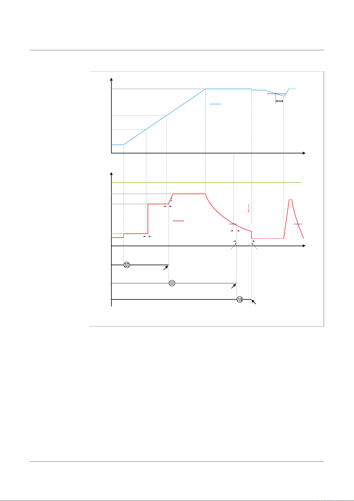
8.10.3 Power-up/down sequence and on-the-fly voltage change
Power-up sequence
PCA9420
Power management IC for low-power microcontroller applications
The device initiates the default power-up sequence in three different conditions.
Condition 1) The device is off with no any power supply (No valid VIN and No battery
with 2.7V or above attached). In this condition, two signals below are able to start the
default power-up sequence.
• A valid VIN supply on VIN pin
• A voltage on ASYS higher than ASYS_UVLO, a 2.8V typical
Condition 2) The device stays off by enabling SHIPMODE or in SHIP mode with a
battery ≥ 2.8V attached. In this condition, two signals are able to start the default powerup sequence.
• A valid VIN supply on VIN pin
• A falling edge on ON key over a 200µs
Condition 3) The device stays off by enabling PWR_DN_EN bit setting to 1 with a
battery ≥ 2.8V attached. In this condition, only one signal is able to start the default
power-up sequence.
• A falling edge on ON key over a 200µs
Condition 4) The device stays at VIN OVP condition with no any valid supply attached
at VBAT. In result, all enabled power rails have been off. The following condition reinitiates the power-up sequence.
• The VIN goes below its VIN OVP hysteresis (typ 100mV)
The power-up sequence by ON key=Low over the debounce time is described as shown
in Figure 6.
For the power-up sequence, the chip can set the default sequence per the customer
requirement at factory setting (i.e. MTP option), from one of the 64 options. Once the chip
enters the power-down stage, the power-down sequence is implemented as the reverse
of the power-up sequence (i.e., first up, last down).
PCA9420 All information provided in this document is subject to legal disclaimers. © NXP B.V. 2021. All rights reserved.
Product data sheet Rev. 2 — 26 January 2021
14 / 82
Page 15
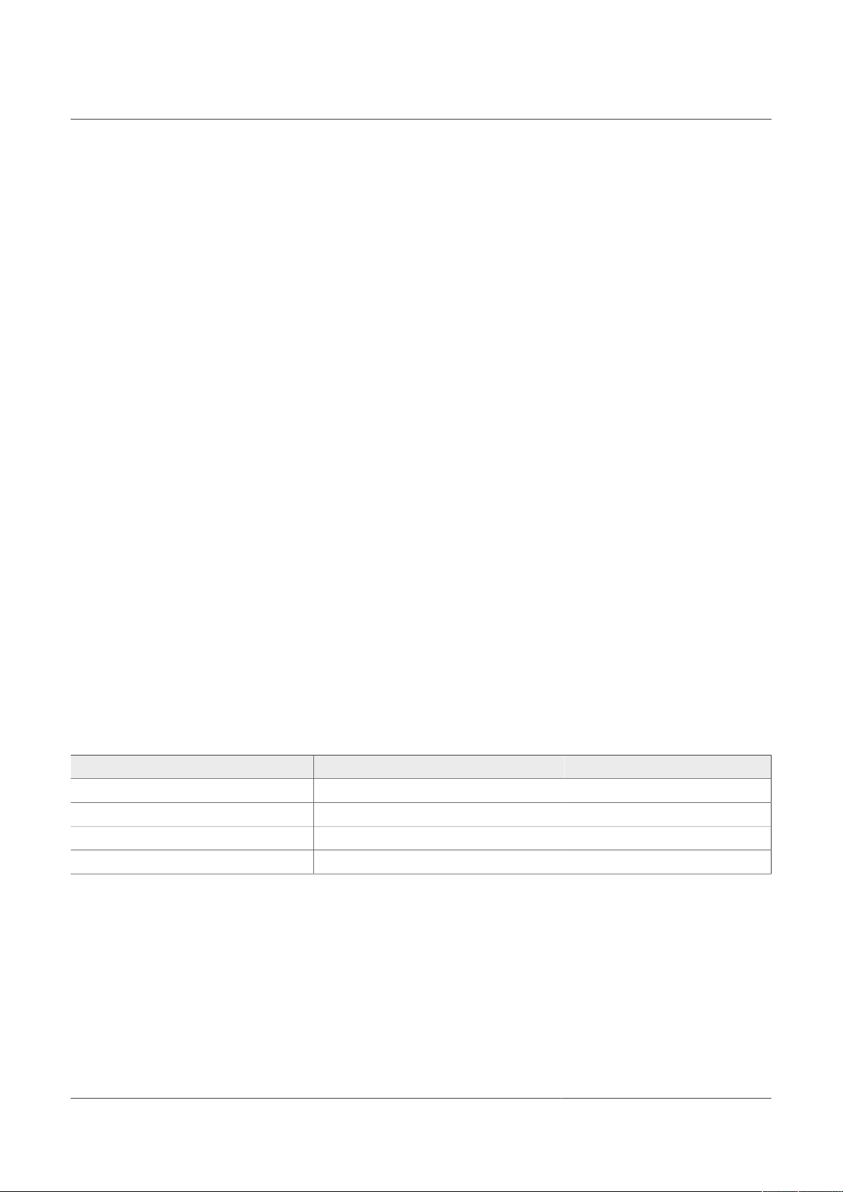
NXP Semiconductors
aaa-033080
POWER-UP SEQUENC
E
ON Key
Default-On Rail
s
Position
1
=1m
s
SYSRSTn
POWER-OFF STATE
CONTROL BY PROCESSOR
T
PWUP_DLY_INTERVAL
(ON Long-Press Timer, 4s,8s,12s or 16s)
t
ON_LONG_PRESS
90%
2
3
4
T
ON_DEBOUNCE
=200µs
NOTE: BUCK1, BUCK2, LDO1 and LDO2 can be assigned to any of position 1-
4
(NOTE
)
3
2
1
=2m
s
The ON Key shall be pulled high
to avoid power recycle initiated
by a programmed ON long-Press
timer expired
PWR_DN_EN bit=1
O
R
SHIP_EN_x bit=1
Position
4
POWER-DOWN SEQUENCE
T
PWDOWN_DLY_INTERVAL
Figure 6. Power-up/down sequence
On-the-fly output voltage change sequence
PCA9420
Power management IC for low-power microcontroller applications
On-the-fly output voltage change is defined as the following: for any output rail, its
output voltage changes from one level (initial level) to another level (target level). Note
this assumes the output rail is always enabled before and after the on-the-fly change
transition. It does not include the case when any output rail is changed from disabled
state to enabled state, or vice versa.
If a user prefers to change any rail voltage on-the-fly, depending on the scenarios listed
below, the chip behavior is described as the following:
1. While the chip remains in its current operation mode, and the user programs the
2. While the user chooses to switch modes, i.e. change mode between any of the two
CAUTION: The user should not send an I2C command related to changing the setting of
the output rails during the power up/down or mode setting change process.
8.10.4 BUCK1 (SW1, core buck regulator)
The SW1 supplies the core power.
Its output voltage can be programmed via I2C from 0.5V to 1.5V at 25mV step and a fixed
1.8V, which is capable of providing up to 250mA loading. The application circuit uses
8.10.5 BUCK2 (SW2, system buck regulator)
typical 2.2µH inductor and 10µF/6.3V output capacitor.
output voltage setting I2C register value or enables/disables any or some of output
voltage rail(s), the chip simply executes the I2C command
mode settings among Mode 0/1/2/3, and if this involves on-the-fly voltage change for
one or some output rails, such change should occur simultaneously when the chip
switches from initial mode to the target mode.
The SW2 output voltage can be programmed via I2C register from 1.5V to 2.1V, or from
2.7V to 3.3V in both at 25mV/step and is capable of providing up to 500mA loading. The
application circuit uses a 2.2µH inductor and 10µF output capacitor.
PCA9420 All information provided in this document is subject to legal disclaimers. © NXP B.V. 2021. All rights reserved.
Product data sheet Rev. 2 — 26 January 2021
15 / 82
Page 16
NXP Semiconductors
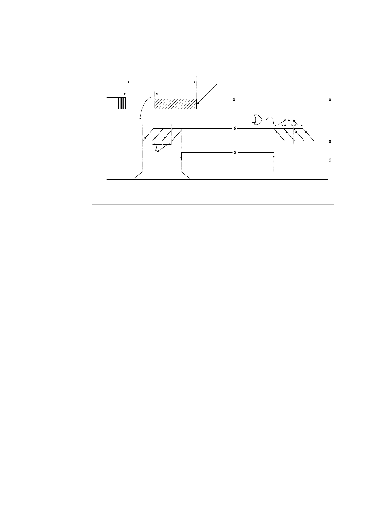
aaa-033081
V
SW2_Regulatio
n
V
PSYS2
(
V
PSYS2
- V
SW2_Regulatio
n
)=200mV
50m
V
SW2 in regulation mode
SW2 in pass-through mo
de
SW2 in regulation mode
Delta V
=R
RDS_ON_High_side
x
I
LOA
D
Delta V
In SW2, a pass-through mode is implemented. When its input (ASYS) is close to the
output voltage (within typical 200mV), the SW2 enters the pass-through mode operation;
the high-side switch is fully turned on and the low-side switch is turned off, and the output
voltage can be calculated as input voltage – (RDSON*I
resistance of the high-side switch, and the I
input voltage rises again, so that the voltage different between input and output crosses
the typical 250mV threshold, the SW2 exits the pass-through mode and re- enters the
normal switching mode operation.
While SW2 operates in pass-through mode, protection features such as over-current
protection are also implemented as well.
PCA9420
Power management IC for low-power microcontroller applications
), where RDSON is the on-
LOAD
refers to the load current. When the
LOAD
Figure 7. Pass-Through mode of BUCK2 (SW2)
8.10.6 LDO1 (always-on LDO)
The LDO1 (Always-on LDO) output can be programmed from 1.7V to 1.9V at 25mV step,
depending on the system requirements (selectable through I2C register). Typically, a
1µF/6.3V MLCC output capacitor providing at least 1mA loading capability is needed.
8.10.7 LDO2 (system LDO)
The LDO2 (system LDO) output can be programmed via the I2C register from 1.5V
to 2.1V, or 2.7V to 3.3V at 25mV/step. Typically, a 2.2µF/6.3V MLCC output capacitor
providing at least 250mA loading current is needed.
8.11 Linear battery charger
The battery charger is a linear charger. Its charging is done through a linear switch with
the following output protections:
• Reverse current protection
– (triggers when VIN < VBAT+ VIN2BAT_HEADROOM*)
• Charging current limiting
– (a function of programmed threshold and battery temperature)
• VBAT short circuit protection
– short circuit output voltage threshold: (typ 0.8V with 80mV hysteresis)
– Maximum output sourcing current during “short circuit” detection ~ 13mA
(VIN2BAT_HEADROOM = 100mV, typical)
PCA9420 All information provided in this document is subject to legal disclaimers. © NXP B.V. 2021. All rights reserved.
Product data sheet Rev. 2 — 26 January 2021
If the battery voltage is below the V
discharged and a preconditioning cycle begins. The amount of pre-charge current
(ICHG_LOW) can be programmed through I2C register setting. This feature is useful
when there is a load connected directly across the battery (at VBAT pin) “stealing” the
BAT_LOW
threshold, the battery is considered
16 / 82
Page 17

NXP Semiconductors
battery current. The pre-charge current can be set higher to account for the system
loading while allowing the battery to be properly conditioned. Once the battery voltage
has charged to the V
charge current (I
using I2C register. The constant current provides the bulk of the charge. Power
dissipation in the device is greatest in fast charge with a lower battery voltage.
If the device reaches a programmed thermal regulation threshold temperature from 85°C
to 115°C in 5°C steps, the device enters thermal regulation. Thermal regulation increases
the safe-charging-timer period by 2x and reduces the charge current in half (if the initial
current is 5mA, it will remain unchanged) to keep the temperature from rising any further
when battery charger works in constant current charging mode, or at a reduced regulated
voltage when battery charger works in constant voltage charging mode.
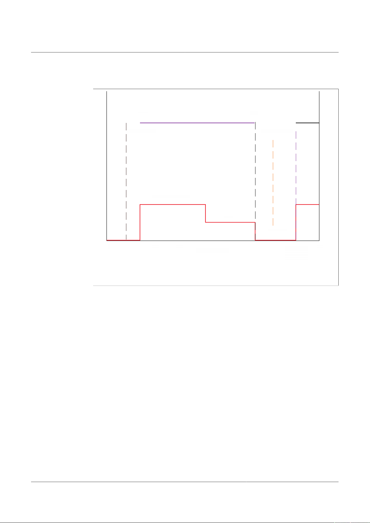
Figure 8 shows the charging profile with a dead battery condition. Once the cell has
charged to the regulation voltage (V
the battery at the regulation voltage until the current tapers to the termination threshold
(I
CHG_TOPOFF
8.11.1 Battery charging management
PCA9420
Power management IC for low-power microcontroller applications
BAT_LOW
CHG_CC
).
threshold, fast charge is initiated and a programmed fast
) is applied. The fast charge constant current is programmed
BAT_REG
) the voltage loop takes control and holds
Battery charging management supports typical constant current/constant voltage
charging profile for single cell Li-Ion battery, as well as pre-qualification (dead battery, low
battery), top-off mode, etc.; JEITA and thermal regulation compliant.
PCA9420 All information provided in this document is subject to legal disclaimers. © NXP B.V. 2021. All rights reserved.
Product data sheet Rev. 2 — 26 January 2021
17 / 82
Page 18
NXP Semiconductors
aaa-033082
VBAT
V
BAT_REG
3.6V to 4.6V, 20mV steps, 4.2V Default
V
BAT_DEA
D
1.9V
(1.7V,1.8V,2V by
MTP)
VBA
T
Trickle Charge
(Dead Battery)
Mode
Fast Charge Mode
Top-OFF
Mode
Charging Done Mode
I
CHG_DEA
D
I
CHG_C
C
Input & Charge Curren
t
Current to battery
I
CHG_TOPO
FF
I
CHG
=0m
A
I
VIN__LI
M
0mA
V
BAT_RESTAR
T
Recharge Mod
e
(Fast Charge Mode)
0V
V
BAT_LOW
2.5V
(2.3V,2.4V,2.6V by MTP)
I
CHG_LOW
t
DGL_BAT_LOW2CC=50µs
Pre-charge
(Low-Voltage
)
Mode
5mA to 315mA programmable in 5mA step
s
t
DGL_BAT_CC2TOPOFF=20ms
(=V
BAT_REG
-140mV or 240mVtyp)
t
DGL_BAT_RESTART
=50ms
I
CHG_TOPOFF
Tim
e
Tim
e
di/dt=3mA/µ
s
85mA to 1105mA programmable
1mA to 63mA programmable
in 1mA steps
1mA to 63mA programmable
in 1mA steps
1mA to 63mA programmabl
e
in 1mA step
s
Shall be updated with 1mA to 20mA Programmabl
e
in 1mA steps due to top-off proble
m
reset
t
DGL_BAT_DEAD2LOW=50µs
T
CHG_FAS
T
T
CHG_TOPOFF
3, 5, 7, or 9 hours
reset
0, 6.4, 12.8, or 19.2min
T
CHG_TOPOFF
starte
d
T
CHG_TOPOFF
expired
T
CHG_TOPOF
F
T
CHG_PRE
Q
15, 30, 45,
or 60mi
n
reset
OFF
O
N
OFF
OFF
O
N
O
N
Fast Charge Mod
e
PCA9420
Power management IC for low-power microcontroller applications
PCA9420 All information provided in this document is subject to legal disclaimers. © NXP B.V. 2021. All rights reserved.
Product data sheet Rev. 2 — 26 January 2021
Figure 8. Typical Charging Profile Example
18 / 82
Page 19
NXP Semiconductors
aaa-033083
Device in non-charging mode
- VIN < VI
N
UVL
O
- CHG_EN=0 or 1
- TJ <
T
J(OFF
)
, 150°C
Any Charging Stat
e
VBAT >
V
BAT_DEA
D
&
&
t
DGL_BAT_DEAD2LOW, 50µs
Charging Stopped
A programmed watchdog timer expired in
nEN_CHG_IN_WATCHDOG=1
&& WD_TIMER_A/B/C/D=2b01, 10, or 1
1
o
r
TJ ≥ a programmed TSHDN
o
r
One of the safety timers (TCHG_PREQ & TCHG_FAST) expire
d
VIN has been validated
&
&
Battery attache
d
&
&
CHG_EN=1
Device in Dead Battery Chargin
g
- Charge current=
I
CHG_DEA
D
- T
CHG_PREQ
started counting
Device in Pre-Charge
(Low Voltage) Mod
e
- Charge current=
I
CHG_LOW
Device in Fast Charge Mode
- Charge current=
I
CHG_C
C
- T
CHG_PREQ
reset
- T
CHG_FAST
started countin
g
VBAT >
V
BAT_LOW
&
&
t
DGL_BAT_LOW2CC, 50µ
s
Device in Top-Off Mod
e
- T
CHG_FAST
reset
- T
CHG_TOPOFF
started countin
g
I
CHG
<
I
CHG_TOPOF
F
for
t
DGL_BAT_CC2TOPOFF, 20ms
T
CHG_TOPOF
F
expire
d
Device in DONE Mo
de
- T
CHG_TOPOFF
reset
- I
CHG
=0mA
I
C
HG
> 2x I
CHG_TOPOFF
or
20mA, whichever is lowe
r
VBAT-
V
BAT_REG
≤
V
BAT_RESTART
, 140mV typ
(240mV by MTP)
&
&
t
DGL_BAT_RESTART, 50ms
TJ = A programmed
T
THEM_REGULATION
Charging in Thermal Regulation
- ICHG= (A programmed
I
CHG_C
C
) x
1_
2
VBAT ≤
V
BAT_DEA
D
VBAT ≤> V
BAT_LOW
&
&
t
DGL_BAT_CC2LOW, 50ms
Any Charging State
PCA9420
Power management IC for low-power microcontroller applications
PCA9420 All information provided in this document is subject to legal disclaimers. © NXP B.V. 2021. All rights reserved.
Product data sheet Rev. 2 — 26 January 2021
Figure 9. Charger State Diagram
19 / 82
Page 20
NXP Semiconductors
aaa-033084
45°C
10°C
Programmed VBAT_REG
0°C
Hot fault
charge disable
No operation
during cold fault
Programmed ICHG
(100%)
50%
Cold fault
0
0.2
VHOT VWARM
0.4
0.6
0.8 1.0
VCOOL
1.2 1.4
VCOLD
1.6
Termination
disable
1.8
TS voltage-V
8.11.2 Battery temperature sensing and JEITA-compliant charging profile
PCA9420
Power management IC for low-power microcontroller applications
Figure 10. Operation over TS bias voltage for JEITA
8.11.3 Low-battery/dead-battery (pre-qualification) charging
If the battery is detected and VBAT < VBAT_LOW, the charger initiates pre-charging
using a predefined (I2C register) current.
When it is under the dead-battery condition, the charging current I
CHG_DEAD
is
programmed by ICHG_DEAD [5:0]; and when it is under the low-battery condition, the
charging current I
CHG_LOW
is programmed by ICHG_LOW [5:0]. When V
BAT
≥ V
BAT_LOW
the charger moves to the next state, fast charging mode.
8.11.4 Constant current charging/constant voltage charging (fast charging) and termination
When V
state, the battery voltage VBAT continues to rise, while the battery is being charged with
the current set by ICHG_CC [5:0], until VBAT reaches the maximum allowable voltage
set by VBAT_REG [5:0].
At this time, the charger enters the Constant Voltage (CV) mode. While operating in
the CV mode, the voltage is still regulated at the level set by VBAT_REG [5:0], and the
charging current continues to decrease.
When the charging current drops below the top-off current threshold, set by
ICHG_TOPOFF [5:0], the charger enters TOPOFF mode, and upon expiration of
TOPOFF timer (set by T_TOPOFF [1:0]), the charger enters DONE mode.
BAT
≥ V
BAT_LOW
, the charger enters Fast Charge Mode (Constant Current). In this
,
PCA9420 All information provided in this document is subject to legal disclaimers. © NXP B.V. 2021. All rights reserved.
Product data sheet Rev. 2 — 26 January 2021
20 / 82
Page 21

NXP Semiconductors
8.11.5 Charger safety timers
Two sets of charging safety timers are implemented on PCA9420. These timers
ensure the charging is terminated if the charging time is longer than its predefined limit
(programmed via I2C registers) at given states:
• Pre-qualification timer, set by ICHG_PREQ_TIMER [1:0], 15min ~ 60min
• Fast charge timer, set by ICHG_FAST_TIMER [1:0], 3hr ~ 9hr
8.11.6 Recharging
While in DONE mode, if the voltage of VBAT stays below (a programmed VBAT_REG –
140mV or 240mV) over the deglitch time (t
resumes back to Constant Current (CC) Mode.
8.11.7 Starting a new charge cycle
When a VIN plug in, VBAT attached, or CHG_EN are set to “1”, the device initializes a
new charging process.
PCA9420
Power management IC for low-power microcontroller applications
DGL_BAT_RESTART
), 50ms the battery charger
8.11.8 Battery attach detection
The device has a unique battery detection scheme with two comparators, 1.9V and 3.4V.
when the detection scheme is executed, a 5mA current sink is activated to determine
battery presence by detection the fall threshold, V
a 5mA current source is used to detect battery voltage whether it stays above the
threshold, V
BAT_DET_UP
, 3.4V. if both conditions are met, absence of battery is declared.
8.12 Hardware and software reset
Please refer to description for ON pin for the hardware reset function by a long time
ON key pressed. The "software reset” is achieved by setting “1” to SW_RST bit in I2C
register. If the user writes a “1” to this bit, it resets all other I2C register bits to their default
setting; this bit is cleared and reset back to “0” as well.
9 I2C-bus interface and register
The PCA9420 implements an I2C-bus slave interface to communicate with the host
system. The interface supports Fast Mode plus Fm+ with up to 1 Mbit/s. A detailed
description of the I2C-bus specification is given in UM10204, Rev. 06, 4 April 2014 ,“ I2Cbus specification and user manual”.
Features such as clock-stretching and 10-bit slave address are not supported; general
call is supported by default but can be disabled via metal option. Auto increment with
address wrap-around is supported as well.
BAT_DET_LOW
, 1.9V typ. In addition,
9.1 I2C slave address
Following a START condition, the bus master must send the target slave address
followed by a read or write operation. The slave address of the PCA9420 is shown below:
PCA9420 All information provided in this document is subject to legal disclaimers. © NXP B.V. 2021. All rights reserved.
Product data sheet Rev. 2 — 26 January 2021
21 / 82
Page 22
NXP Semiconductors
PCA9420
Power management IC for low-power microcontroller applications
Table 6. I2C Slave Address
Bit 7 Bit 6 Bit 5 Bit 4 Bit 3 Bit 2 Bit 1 Bit 0
1 1 0 0 0 0 1 0/1
Fixed Fixed Fixed MTP option Fixed Fixed Fixed R/W
Bit 4 should be reserved as MTP option, with its default value set as “0” but can be
trimmed to “1” when needed.
9.2 General call and device ID addresses
The device implements two different addresses for general call and device ID.
9.3 Register type
There are four register types used on the device:
• Read and Write (R/W)
• Read Only (R)
• Write Only (W)
• Write and Clear (W/C)
For Write and Clear (W/C), a write to a register with a bit-mask specifies which interrupts
to clear.
For example, if the status register shows 8’b0000_1001 as an interrupt status (i.e.
interrupt [0] and interrupt [3] are both set), user may write 8’b0000_1000, meaning the
intent is to only clear interrupt [3] (but interrupt [0] should NOT be “cleared”). If the intent
is to clear both interrupts, then the user could write back 8’b0000_1001.
9.4 Register map
Table 7. Register map
Address
(Hex)
System Control Registers
00 Device Information, DEV_INFO Device ID, revision R 0000 0000
01 Top Level Interrupt Status, TOP_INT Top level interrupt event status R/C 0000 0000
02 Sub Level Interrupt_0, SUB_INT0 Sub-level interrupt indication_0 W/C 0000 0000
03 Sub Level Interrupt_0 Mask, SUB_
04 Sub Level Interrupt_1, SUB_INT1 Sub-level interrupt indication_1 W/C 0000 0000
05 Sub Level Interrupt_1 Mask, SUB_
06 Sub Level Interrupt_2, SUB_INT2 Sub-level interrupt indication_2 W/C 0000 0000
07 Sub Level Interrupt_2 Mask, SUB_
08 RSVD Reserved R/W 0000 0000
09 Top Level Control_0, TOP_CNTL0 Top level system control_0 R/W 0100 0001
Register Name Description Type Reset
Value
(Binary)
INT0_MASK
INT1_MASK
INT2_MASK
Sub-level interrupt mask for SUB_
INT0
Sub-level interrupt mask for SUB_
INT1
Sub-level interrupt mask for SUB_
INT2
R/W 0011 1111
R/W 0111 1111
R/W 1111 1111
PCA9420 All information provided in this document is subject to legal disclaimers. © NXP B.V. 2021. All rights reserved.
Product data sheet Rev. 2 — 26 January 2021
22 / 82
Page 23
NXP Semiconductors
PCA9420
Power management IC for low-power microcontroller applications
Table 7. Register map...continued
Address
(Hex)
0A Top Level Control_1, TOP_CNTL1 Top level system control_1 R/W 1000 1001
0B Top Level Control_2, TOP_CNTL2 Top level system control_2 R/W 1100 1110
0C Top Level Control_3, TOP_CNTL3 Top level system control_3 R/W 0000 0001
0D Top Level Control_4, TOP_CNTL4 Top level system control_4 W 0000 0000
0E – 0F RSVD Reserved
Battery Charger Control
10 Battery Charger Control_0, CHG_
11 Battery Charger Control_1, CHG_
12 Battery Charger Control_2, CHG_
13 Battery Charger Control_3, CHG_
14 Battery Charger Control_4, CHG_
15 Battery Charger Control_5, CHG_
16 Battery Charger Control_6, CHG_
17 Battery Charger Control_7, CHG_
18 Battery Charger Status_0, CHG_
19
1A
1B
1C – 1F RSVD Reserved
Regulator Control
20 Regulator Status, REG_STATUS Regulators status indication R 0000 0000
21
22
23
24
Register Name Description Type Reset
Value
(Binary)
Battery charger control register_0 R/W 0000 0011
CNTL0
Battery charger control register_1 R/W 0000 1000
CNTL1
Battery charger control register_2 R/W 0000 0100
CNTL2
Battery charger control register_3 R/W 0000 1000
CNTL3
Battery charger control register_4 R/W 0000 0100
CNTL4
Battery charger control register_5 R/W 0001 1110
CNTL5
Battery charger control register_6 R/W 1001 0101
CNTL6
Battery charger control register_7 R/W 0010 0100
CNTL7
Battery charger status indication_0 R 0001 0000
STATUS_0
Battery Charger Status_1, CHG_
STATUS_1
Battery Charger Status_2, CHG_
STATUS_2
Battery Charger Status_3, CHG_
STATUS_3
Active Discharge Control, ACT_
DISCHARGE_CNTL_1
Mode Configuration Mode Setting 0_
0, MODECFG_0_0
Mode Configuration Mode Setting 0_
1, MODECFG_0_1
Mode Configuration Mode Setting 0_
2, MODECFG_0_2
Battery charger status indication_1 R 0000 0000
Battery charger status indication_2 R 0111 1000
Battery charger status indication_3 R 0000 0000
Active Discharge control register R/W 0000 0000
Mode configuration settings for
Mode 0_0
Mode configuration settings for
Mode 0_1
Mode configuration settings for
Mode 0_2
R/W 0001 0100
R/W 0000 1100
R/W 0100 1111
PCA9420 All information provided in this document is subject to legal disclaimers. © NXP B.V. 2021. All rights reserved.
Product data sheet Rev. 2 — 26 January 2021
23 / 82
Page 24
NXP Semiconductors
Table 7. Register map...continued
Address
(Hex)
25
26
27
28
29
2A
2B
2C
2D
2E
2F
30
31
Register Name Description Type Reset
Mode Configuration Mode Setting 0_
3, MODECFG_0_3
Mode Configuration Mode Setting 1_
0, MODECFG_1_0
Mode Configuration Mode Setting 1_
1, MODECFG_1_1
Mode Configuration Mode Setting 1_
2, MODECFG_1_2
Mode Configuration Mode Setting 1_
3, MODECFG_1_3
Mode Configuration Mode Setting 2_
0, MODECFG_2_0
Mode Configuration Mode Setting 2_
1, MODECFG_2_1
Mode Configuration Mode Setting 2_
2, MODECFG_2_2
Mode Configuration Mode Setting 2_
3, MODECFG_2_3
Mode Configuration Mode Setting 3_
0, MODECFG_3_0
Mode Configuration Mode Setting 3_
1, MODECFG_3_1
Mode Configuration Mode Setting 3_
2, MODECFG_3_2
Mode Configuration Mode Setting 3_
3, MODECFG_3_3
PCA9420
Power management IC for low-power microcontroller applications
Value
(Binary)
Mode configuration settings for
Mode 0_3
Mode configuration settings for
Mode 1_0
Mode configuration settings for
Mode 1_1
Mode configuration settings for
Mode 1_2
Mode configuration settings for
Mode 1_3
Mode configuration settings for
Mode 2_0
Mode configuration settings for
Mode 2_1
Mode configuration settings for
Mode 2_2
Mode configuration settings for
Mode 2_3
Mode configuration settings for
Mode 3_0
Mode configuration settings for
Mode 3_1
Mode configuration settings for
Mode 3_2
Mode configuration settings for
Mode 3_3
R/W 0011 1001
R/W 0001 1100
R/W 0100 1100
R/W 0100 1111
R/W 0000 1100
R/W 0001 1100
R/W 0100 1100
R/W 0100 1111
R/W 0000 1100
R/W 0001 1100
R/W 0100 1100
R/W 0100 1111
R/W 0000 1100
9.5 Register description
9.5.1 Device information (DEV_INFO, address 00h)
The device identification code stores a unique identifier for each version and/or revision
of device, so that the connected MCU recognizes it automatically.
This is a READ ONLY register.
Table 8. DEV_INFO register bit description
Bit Symbol Default value Type Function
7 DEV_ID [4] 0 R
6 DEV_ID [3] 0 R
5 DEV_ID [2] 0 R
4 DEV_ID [1] 0 R
PCA9420 All information provided in this document is subject to legal disclaimers. © NXP B.V. 2021. All rights reserved.
Product data sheet Rev. 2 — 26 January 2021
Device ID
24 / 82
Page 25
NXP Semiconductors
Power management IC for low-power microcontroller applications
Table 8. DEV_INFO register bit description...continued
Bit Symbol Default value Type Function
3 DEV_ID [0] 0 R
2 DEV_REV [2] 0 R
1 DEV_REV [1] 0 R
0 DEV_REV [0] 0 R
9.5.2 Top level interrupt status (TOP_INT, address 01h)
The top-level interrupt register contains flags indicating various top level interrupt events
as indicated below. An event will be latched and only its first occurrence triggers the
interrupt signal INTB (if it is not being masked). Reoccurring events will not change the
flag's status or trigger an additional interrupt. If multiple interrupt events happen, its
corresponding interrupt bits in the related registers will be “triggered”, however, the INTB
signal will be only triggered upon the first interrupt event.
The interrupt event reporting on the device is structured in a two-layer configuration. The
interrupt events are grouped as (1) system level; (2) charger block; (3) buck regulator
block; (4) LDO block. When any interrupt event is triggered, based on which mode it
falls into, the related bit for that mode in TOP_INT flags “1”. Any of the related bits in
TOP_INT will only change back to 0 when all the interrupt events in its affiliated mode
have been cleared.
Device revision
PCA9420
This is READ Only register.
Table 9. TOP_INT register bit description
Bit Symbol Default value Type Function
7 RSVD 0 R Reserved bit
6 RSVD 0 R Reserved bit
5 RSVD 0 R Reserved bit
4 RSVD 0 R Reserved bit
3 SYS_INT 0 R System level interrupt event trigger indication 0: no system level
interrupt event triggered 1: system level interrupt event triggered
2 CHG_INT 0 R Linear battery charger block interrupt event trigger indication 0: no
linear battery charger block interrupt event triggered
1: linear battery charger block interrupt event triggered
1 SW_INT 0 R Buck regulator blocks (SW1, SW2) interrupt event trigger indication 0:
no interrupt event on SW1 and/or SW2 blocks triggered
1: interrupt event on SW1 and/or SW2 blocks triggered
0 LDO_INT 0 R LDO block (LDO1, LDO2) interrupt event trigger indication 0: no
interrupt event on LDO1 and/or LDO2 blocks triggered 1: interrupt
event on LDO1 and/or LDO2 blocks triggered
9.5.3 Sub level interrupt_0 (SUB_INT0, address 02h)
The sub-level interrupt register contains flags indicating the second-tier interrupt event.
For this register, it contains system level related interrupt events.
This is WRITE AND CLEAR register.
PCA9420 All information provided in this document is subject to legal disclaimers. © NXP B.V. 2021. All rights reserved.
Product data sheet Rev. 2 — 26 January 2021
25 / 82
Page 26

NXP Semiconductors
Power management IC for low-power microcontroller applications
Table 10. Sub_INT0 register bit description
Bit Symbol Default value Type Function
7 RSVD 0 W/C Reserved bit
6 RSVD 0 W/C Reserved bit
5 ON_PUSH_INT 0 W/C ON falling edge longer than 5ms happened
4 TEMP_
PREWARNING
3 THEM_SHDN 0 W/C Thermal shutdown interrupt
2 ASYS_
PREWARNING
1 WD_TIMER 0 W/C Watchdog Timer Expiration Interrupt:
0 VIN 0 W/C Input Voltage Interrupt
0 W/C Die temperature pre-warning interrupt
1: die temp ≥ TWARNING; 0: die temp < TWARNING TWARNING
threshold is configured by T_WARNING [1:0]
0: thermal shutdown is not triggered
1: die temp ≥ TSHDN (set in THEM_SHDN [2:0], thermal shutdown is
triggered
0 W/C ASYS Pre-Warning Voltage Interrupt:
0: ASYS voltage does NOT fall below the threshold set in ASYS_
PREWARNING [1:0]
1: ASYS voltage falls below the threshold set in ASYS_PREWARNING
[1:0]
0: The watchdog timer expiration has not happened since the last time
this bit was cleared.
1: The watchdog timer expiration has happened since the last time this
bit was cleared.
0: The VIN_OK bit has not changed since the last time this bit was
cleared.
1: The VIN _OK bit has changed since the last time this bit was
cleared.
PCA9420
9.5.4 Sub level interrupt_0 mask (Sub_INT0_Mask, address 03h)
This is a READ AND WRITE register.
Table 11. Sub_INT0_Mask bit description
Bit Symbol Default
value
7 RSVD 0 R/W Reserved bit
6 RSVD 0 R/W Reserved bit
5 ON_PUSH_INT_MASK 1 R/W ON Key falling interrupt mask bit
4 TEMP_PREWARNING_MASK 1 R/W Die temp pre-warning interrupt mask bit
3 THEM_SHDN_MASK 1 R/W Thermal shutdown interrupt mask bit
PCA9420 All information provided in this document is subject to legal disclaimers. © NXP B.V. 2021. All rights reserved.
Product data sheet Rev. 2 — 26 January 2021
Type Function
0: Not Masked
1: Masked
0: Not Masked
1: Masked
0: Not Masked
1: Masked
26 / 82
Page 27

NXP Semiconductors
PCA9420
Power management IC for low-power microcontroller applications
Table 11. Sub_INT0_Mask bit description...continued
Bit Symbol Default
value
2 ASYS_PREWARNING_MASK 1 R/W ASYS Pre-Warning Voltage Interrupt Mask bit
1 WD_TIMER_MASK 1 R/W Watchdog Timer Expiration Interrupt Mask bit
0 VIN_MASK 1 R/W Input Voltage Interrupt Mask bit
Type Function
0: Not Masked
1: Masked
0: Not Masked
1: Masked
0: Not Masked
1: Masked
9.5.5 Sub level interrupt_1 (Sub_INT1, address 04h)
The sub-level interrupt register contains flags indicating the second-tier interrupt event.
For this register, it contains battery charger related interrupt events.
This is WRITE AND CLEAR register.
Table 12. Sub_INT1 register bit description
Bit Symbol Default value Type Function
7 RSVD 0 W/C Reserved bit
6 RSVD 0 W/C Reserved bit
5 VIN_ILIM 0 W/C Input Current Limit Interrupt:
0: no Input current limit has been triggered since the last
time this bit is cleared;
1: input current limit event is triggered since last time this bit
is cleared.
4 ICHG_FAST_TIMER 0 W/C Fast Charging Timer Expiration Interrupt:
0: The fast charging timer expiration has not happened
since the last time this bit was cleared.
1: The fast charging timer expiration has happened since
the last time this bit was cleared.
3 ICHG_PREQ_TIMER 0 W/C Pre-qualification Charging Timer Expiration Interrupt:
0: The pre-qual charging timer expiration has not happened
since the last time this bit was cleared.
1: The pre-qual charging timer expiration has happened
since the last time this bit was cleared.
2 BATTERY_DETECTION 0 W/C Battery presence Interrupt
0: The VBAT_DET_OK bit has not changed since the last
time this bit was cleared.
1: The VBAT_DET_OK bit has changed since the last time
this bit was cleared.
1 VBAT 0 W/C Battery Interrupt
0: The VBAT_OK bit has not changed since the last time
this bit was cleared.
1: The VBAT_OK bit has changed since the last time this bit
was cleared.
PCA9420 All information provided in this document is subject to legal disclaimers. © NXP B.V. 2021. All rights reserved.
Product data sheet Rev. 2 — 26 January 2021
27 / 82
Page 28

NXP Semiconductors
PCA9420
Power management IC for low-power microcontroller applications
Table 12. Sub_INT1 register bit description...continued
Bit Symbol Default value Type Function
0 CHG_OK 0 W/C Charger Status Interrupt
0: The CHG_OK bit has not changed since the last time this
bit was cleared.
1: The CHG_OK bit has changed since the last time this bit
was cleared
9.5.6 Sub level interrupt_1 mask (Sub_INT1_Mask, address 05h)
This is a READ AND WRITE register.
Table 13. Sub_INT1_Mask register bit description
Bit Symbol Default
value
7 RSVD 0 R/W Reserved bit
6 RSVD 1 R/W Reserved bit
5 VIN_ILIM_MASK 1 R/W Input Current Limit Interrupt Mask bit
4 ICHG_FAST_TIMER_MASK 1 R/W Fast Charging Timer Expiration Interrupt Mask bit
3 ICHG_PREQ_TIMER_MASK 1 R/W Pre-qual Charging Timer Expiration Interrupt Mask bit
2 BATTERY_DETECTION_MASK 1 R/W Battery presence Interrupt Mask bit
1 VBAT_MASK 1 R/W Battery Interrupt Mask bit
0 CHG_OK_MASK 1 R/W Charger Interrupt Mask bit
Type Function
0: Not Masked
1: Masked
0: Not Masked
1: Masked
0: Not Masked
1: Masked
0: Not Masked
1: Masked
0: Not Masked
1: Masked
0: Not Masked
1: Masked
9.5.7 Sub level interrupt_2 (Sub_INT2, address 06h)
The sub-level interrupt register contains flags indicating the second-tier interrupt event.
For this register, it contains LDO1/LDO2, SW1/SW2 related interrupt events.
This is WRITE AND CLEAR register.
Table 14. Sub_INT2 register bit description
Bit Symbol Default value Type Function
7 RSVD 0 W/C Reserved bit
6 RSVD 0 W/C Reserved bit
5 RSVD 0 W/C Reserved bit
PCA9420 All information provided in this document is subject to legal disclaimers. © NXP B.V. 2021. All rights reserved.
Product data sheet Rev. 2 — 26 January 2021
28 / 82
Page 29

NXP Semiconductors
Power management IC for low-power microcontroller applications
Table 14. Sub_INT2 register bit description...continued
Bit Symbol Default value Type Function
4 RSVD 0 W/C Reserved bit
3 VOUTSW1 0 W/C SW1 Output Voltage Interrupt
0: The VOUTSW1_OK bit has not changed since the last time this bit
was cleared.
1: The VOUTSW1_OK bit has changed since the last time this bit was
cleared.
2 VOUTSW2 0 W/C SW2 Output Voltage Interrupt
0: The VOUTSW2_OK bit has not changed since the last time this bit
was cleared.
1: The VOUTSW2_OK bit has changed since the last time this bit was
cleared.
1 VOUTLDO1 0 W/C LDO1 Output Voltage Interrupt
0: The VOUTLDO1_OK bit has not changed since the last time this bit
was cleared.
1: The VOUTLDO1_OK bit has changed since the last time this bit was
cleared.
0 VOUTLDO2 0 W/C LDO2 Output Voltage Interrupt
0: The VOUTLDO2_OK bit has not changed since the last time this bit
was cleared.
1: The VOUTLDO2_OK bit has changed since the last time this bit was
cleared.
PCA9420
9.5.8 Sub level interrupt_2 mask (Sub_INT2_Mask, address 07h)
This is a READ AND WRITE register.
Table 15. Sub_INT2_Mask register bit description
Bit Symbol Default value Type Function
7 RSVD 1 R/W Reserved bit
6 RSVD 1 R/W Reserved bit
5 RSVD 1 R/W Reserved bit
4 RSVD 1 R/W Reserved bit
3 VOUTSW1 _MASK 1 R/W VOUTSW1 Voltage Interrupt Mask bit
0: Not Masked
1: Masked
2 VOUTSW2 _MASK 1 R/W VOUTSW2 Voltage Interrupt Mask bit
0: Not Masked
1: Masked
1 VOUTLDO1 _MASK 1 R/W VOUTLDO1 Voltage Interrupt Mask bit
0: Not Masked
1: Masked
0 VOUTLDO2_MASK 1 R/W VOUTLDO2 Voltage Interrupt Mask bit
0: Not Masked
1: Masked
08h register: Reserved
PCA9420 All information provided in this document is subject to legal disclaimers. © NXP B.V. 2021. All rights reserved.
Product data sheet Rev. 2 — 26 January 2021
29 / 82
Page 30

NXP Semiconductors
PCA9420
Power management IC for low-power microcontroller applications
9.5.9 Top level control_0 (TOP_CTL0, address 09h)
This register contains various configuration bits for top level related functions, part 0. This
is a READ AND WRITE register.
Table 16. TOP_CNTL0 register bit description
Bit Symbol Default value Type Function
7
VIN_ILIM_SEL
[2:0]
6
5
4 OPERATION_SEL_
FROM_SHIPMODE
3 PWR_DN_EN
2 nEN_CHG_IN_
WATCHDOG
1 RSVD 0 R/W Reserved bit
0 PGood_EN 1 R/W LDO1, LDO2, SW1, SW2 Output Voltage Status Indication
[1]
010 R/W VIN input current limit selection: (min/typ/max)
000: 74mA/85mA/98mA, (another default setting by MTP)
001: 222mA/255mA/293mA
010: 370mA/425mA/489mA (default setting)
011: 517mA/595mA/684mA
100: 665mA/765mA/880mA
101: 813mA/935mA/1075mA
110: 961mA/1105mA/1271mA
111: Input current limit disabled
[Note] 1-bit MTP, VIN_ILIM_SEL [1], should be reserved to
change the default value for this function
0 R/W Ship mode wakeup configuration setting
0: upon VIN plug in, the chip will enable the battery charging
process, AND start the power-up sequence for LDO1/LDO2/
SW1/SW2 per the setting
1: upon VIN plug in, the chip will enable the charging process,
LDO1/LDO2/SW1/SW2 remain in shutdown mode and the chip
will only enable the power-up sequence upon ON pin falling
edge
[Note] 1-bit MTP should be reserved to change the default value
for this function
0 R/W Power-down Sequence Enable
0: Do not start power-down sequence
1: Start power-down sequence
0 R/W Configure operations in a programmed watchdog timer expired
0: When the programmed watchdog timer expires, the following
operations take place.
• SYSRSTn signal asserts (high to low)
• Charging is continued
• LDO1/LDO2/SW1/SW2 enters the mode 0 setting
1: When the programmed watchdog timer expires, the following
operations take place.
• SYSRSTn signal asserts (high to low)
• Charging is disabled
• LDO1/LDO2/SW1/SW2 enters the mode 0 setting
0: Output voltage power-good comparators are disabled.
This will also set “VOUTSW1 _OK”, “VOUTSW2 _OK”,
“VOUTLDO1_OK” and “VOUTLDO2 _OK” bits to 0
1: Output voltage power-good comparators are enabled
[1] A valid VIN does not generate the initial power-up sequence if all power rails have been turned off by setting PWR_DN_EN to 1. The use of PWR_DN_EN
bit is prohibited to be used in any application that requires power-up sequence by both VIN and ON key.
PCA9420 All information provided in this document is subject to legal disclaimers. © NXP B.V. 2021. All rights reserved.
Product data sheet Rev. 2 — 26 January 2021
30 / 82
Page 31

NXP Semiconductors
PCA9420
Power management IC for low-power microcontroller applications
The use of SHIP_EN_x (x can be 0, 1, 2 &3) is recommended for the application.
9.5.10 Top level control_1 (TOP_CTL1, address 0Ah)
This register contains various configuration bits for top level related functions, part 1. This
is a READ AND WRITE register.
Table 17. TOP_CNTL1 register bit description
Bit Symbol Default
value
7
ASYS_PREWARNING
[1:0]
6
5
ASYS_INPUT_SEL
[1:0]
4
3 RSVD 1 R/W Reserved bit
2 VIN_OVP_SEL 0 R/W VIN over-voltage protection threshold (rising) selection
1
VIN_UVLO_SEL
[1:0]
0
10 R/W ASYS Program a pre-warning voltage threshold on ASYS
00 R/W ASYS input source selection
01 R/W Program an under-voltage lockout threshold (falling) on VIN
Type Function
00: 3.3V
01: 3.4V
10: 3.5V
11: 3.6V
00: ASYS is power by either VBAT or VIN (VIN has higher
priority over VBAT if both are presented)
01: ASYS is powered by VBAT only
10: ASYS is powered by VIN only
11: ASYS is disconnected to either VBAT or VIN (for internal
testing purpose only)
0: 5.50V
1: 6.0V
Note: The current default value for VIN_OVP_SEL is set
at 5.5V, but it should be MTP programmable
00: 2.9V
01: 3.1V
10: 3.3V
11: 3.5V
9.5.11 Top level control_2 (TOP_CTL2, address 0Bh)
This register contains various configuration bits for top level related functions, part 2. This
is a READ AND WRITE register.
Table 18. TOP_CNTL2 register bit description
Bit Symbol Default value Type Function
7
ASYS_UVLO_SEL
[1:0]
6
5 TERM_DIS 0 R/W Enable/Disable the charge termination control. In this mode,
PCA9420 All information provided in this document is subject to legal disclaimers. © NXP B.V. 2021. All rights reserved.
Product data sheet Rev. 2 — 26 January 2021
11 R/W Program a UVLO threshold on ASYS
00: 2.4V
01: 2.5V
10: 2.6V
11: 2.7V
the fast charge timer is reset.
0: Enable charge termination mode
1: Disable charge termination mode
31 / 82
Page 32

NXP Semiconductors
Power management IC for low-power microcontroller applications
Table 18. TOP_CNTL2 register bit description...continued
Bit Symbol Default value Type Function
4
THEM_SHDN
[2:0]
3
2
1
DIE_TEMP_WARNING
[1:0]
0
011 R/W Program a thermal shutdown threshold, TSHDN, in
rising(hysteresis with 20°C)
000: 95°C
001: 100°C
010: 105°C
011: 110°C
100: 115°C
101: 120°C
110: 125°C
111: reserved
10 R/W Program a Die temperature warning threshold
00: 75°C
01: 80°C
10: 85°C
11: 90°C
PCA9420
9.5.12 Top level control_3 (TOP_CTL3, address 0Ch)
This register contains various configuration bits for top level related functions, part 3. This
is a READ AND WRITE register.
Table 19. TOP_CNTL3 register bit description
Bit Symbol Default value Type Function
7 RSVD 0 R/W Reserved bit
6 RSVD 0 R/W Reserved bit
5 RSVD 0 R/W Reserved bit
4 MODE1_I2C 0 R/W
3 MODE0_I2C 0 R/W
2 SW_RST 0 W/C Chip software reset bit. If user write “1” to this bit, it will reset all other
1
0
ON_GLT_LONG
[1:0]
01 R/W Program a long glitch timer on ON key
Depending on EN_MODE_SEL_BY_PIN_x (x=”0”, or “1”, or “2”,
or “3”) bit setting, the chip mode control is set by either the I2C bit
MODE1_I2C/ MODE0_I2C value, or the signal applied on external
MODESEL1/ MODESEL1 pins. Refer to EN_MODE_SEL_BY_PIN
description for more details.
With EN_MODE_SEL_BY_PIN=0, the mode selection is determined
by the following:
[MODE1_I2C: MODE0_I2C] = 00, mode 0 setting
[MODE1_I2C: MODE0_I2C] = 01, mode 1 setting
[MODE1_I2C: MODE0_I2C] = 10, mode 2 setting
[MODE1_I2C: MODE0_I2C] = 11, mode 3 setting
I2C register bit to its default setting and cycle the regulator outputs,
and meanwhile, this bit will be clear and reset back to “0” as well.
00: 4s
01: 8s
10: 12s
11: 16s
Note: 2-bit MTP should be reserved to change the default setting
PCA9420 All information provided in this document is subject to legal disclaimers. © NXP B.V. 2021. All rights reserved.
Product data sheet Rev. 2 — 26 January 2021
32 / 82
Page 33

NXP Semiconductors
Power management IC for low-power microcontroller applications
9.5.13 Top level control_4 (TOP_CTL4, address 0Dh)
This register contains various configuration bits for top level related functions, part 4. This
is a WRITE ONLY register.
Table 20. TOP_CNTL4 register bit description
Bit Symbol Default value Type Function
7
6
5
4
3
2
1
0
RSVD 00000 W Reserved bit
WD_TIMER_CLR
[2:0]
000 W Watchdog Timer Reset.
001: When written 001 to WD_TIMER_CLR [2:0], the watchdog timer
is reset.
All other values: when written to WD_TIMER_CLR [2:0], watchdog
timer remains unaffected.
PCA9420
9.5.14 Battery charger control_0 (CHG_CTL0, address 10h)
This register stores the linear battery charge related control registers, part 0. This is a
READ AND WRITE register.
Table 21. CHG_CNTL0 register bit description
Bit Symbol Default value Type Function
7
6
5
4
3
2 NTC_EN 0 R/W Enable TS pin external thermistor (NTC) control in charger
1 CHG_TIMER_EN 1 R/W Enable the fast charge timer and pre-qual timer
0 CHG_EN 1 R/W Enable the linear battery charger
CHG_LOCK
[4:0]
00000 R/W Critical charger related setting lock.
CHG_LOCK [4:0] = 10101, these registers which are labeled as
“locked by CHG_LOCK” can be accessed to perform I2C “write”
command.
CHGN_LOCK [4:0] ≠ 10101, these registers which are labeled as
“locked by CHG_LOCK” can NOT be accessed to perform I2C “write”
command. In such case when “write” command is performed on these
locked registers, it will keep the present register value.
0: Disable Thermistor (NTC) control in charger
1: Enable Thermistor (NTC) control in charger
0: Disable both fast charge timer and pre-qual timer
1: Enable both fast charge timer and pre-qual timer
0: Disable charger
1: Enable charger
Note: The default value for this bit should be MTP programmable
9.5.15 Battery charger control_1 (CHG_CTL1, address 11h)
This register stores the linear battery charge related control registers, part 1.
This is a READ AND WRITE register, and this register is locked by CHG_LOCK.
PCA9420 All information provided in this document is subject to legal disclaimers. © NXP B.V. 2021. All rights reserved.
Product data sheet Rev. 2 — 26 January 2021
33 / 82
Page 34

NXP Semiconductors
PCA9420
Power management IC for low-power microcontroller applications
Table 22. CHG_CNTL1 register bit description
Bit Symbol Default value Type Function
7 RSVD 0 R/W Reserved bit
6 RSVD 0 R/W Reserved bit
5
4
3
2
1
0
Table 23. Linear battery charger constant current (CC) setting
00h: 0mA 10h: 80mA 20h: 160mA 30h: 240mA
01h: 5mA 11h: 85mA 21h: 165mA 31h: 245mA
02h: 10mA 12h: 90mA 22h: 170mA 32h: 250mA
03h: 15mA 13h: 95mA 23h: 175mA 33h: 255mA
04h: 20mA 14h: 100mA 24h: 180mA 34h: 260mA
05h: 25mA 15h: 105mA 25h: 185mA 35h: 265mA
06h: 30mA 16h: 110mA 26h: 190mA 36h: 270mA
07h: 35mA 17h: 115mA 27h: 195mA 37h: 275mA
08h: 40mA (default) 18h: 120mA 28h: 200mA 38h: 280mA
09h: 45mA 19h: 125mA 29h: 205mA 39h: 285mA
0Ah: 50mA 1Ah: 130mA 2Ah: 210mA 3Ah: 290mA
0Bh: 55mA 1Bh: 135mA 2Bh: 215mA 3Bh: 295mA
0Ch: 60mA 1Ch: 140mA 2Ch: 220mA 3Ch: 300mA
0Dh: 65mA 1Dh: 145mA 2Dh: 225mA 3Dh: 305mA
0Eh: 70mA 1Eh: 150mA 2Eh: 230mA 3Eh: 310mA
0Fh: 75mA 1Fh: 155mA 2Fh: 235mA 3Fh: 315mA
ICHG_CC
[5:0]
001000 R/W Program a fast charge current
Note: The current default value for ICHG_CC [5:0] is set at 40mA,
but it should be MTP programmable.
9.5.16 Battery charger control_2 (CHG_CTL2, address 12h)
This register stores the present status of chip, part 2, linear battery charger related
status. This is a READ AND WRITE register, and this register is locked by
CHG_LOCK.
Table 24. CHG_CNTL2 register bit description
Bit Symbol Default value Type Function
7 RSVD 0 R/W Reserved bit
6 RSVD 0 R/W Reserved bit
PCA9420 All information provided in this document is subject to legal disclaimers. © NXP B.V. 2021. All rights reserved.
Product data sheet Rev. 2 — 26 January 2021
34 / 82
Page 35

NXP Semiconductors
PCA9420
Power management IC for low-power microcontroller applications
Table 24. CHG_CNTL2 register bit description...continued
Bit Symbol Default value Type Function
5
4
3
2
1
0
Table 25. Linear battery charger top-off charge current setting
00h: 0mA 10h: 16mA 20h: 32mA 30h: 48mA
01h: 1mA 11h: 17mA 21h: 33mA 31h: 49mA
02h: 2mA 12h: 18mA 22h: 34mA 32h: 50mA
03h: 3mA 13h: 19mA 23h: 35mA 33h: 51mA
04h: 4mA (default) 14h: 20mA 24h: 36mA 34h: 52mA
05h: 5mA 15h: 21mA 25h: 37mA 35h: 53mA
06h: 6mA 16h: 22mA 26h: 38mA 36h: 54mA
07h: 7mA 17h: 23mA 27h: 39mA 37h: 55mA
08h: 8mA 18h: 24mA 28h: 40mA 38h: 56mA
09h: 9mA 19h: 25mA 29h: 41mA 39h: 57mA
0Ah: 10mA 1Ah: 26mA 2Ah: 42mA 3Ah: 58mA
0Bh: 11mA 1Bh: 27mA 2Bh: 43mA 3Bh: 59mA
0Ch: 12mA 1Ch: 28mA 2Ch: 44mA 3Ch: 60mA
0Dh: 13mA 1Dh: 29mA 2Dh: 45mA 3Dh: 61mA
0Eh: 14mA 1Eh: 30mA 2Eh: 46mA 3Eh: 62mA
0Fh: 15mA 1Fh: 31mA 2Fh: 47mA 3Fh: 63mA
ICHG_TOPOFF
[5:0]
000100b R/W Program a top-off current
Note: The current default value for ICHG_TOPOFF [5:0] is set at
4mA, but it should be MTP programmable.
9.5.17 Battery charger control_3 (CHG_CTL3, address 13h)
This register stores the present status of chip, part 3, linear battery charger related
status. This is a READ AND WRITE register, and this register is locked by
CHG_LOCK.
Table 26. CHG_CNTL3 register bit description
Bit Symbol Default value Type Function
7 RSVD 0 R/W Reserved bit
6 RSVD 0 R/W Reserved bit
PCA9420 All information provided in this document is subject to legal disclaimers. © NXP B.V. 2021. All rights reserved.
Product data sheet Rev. 2 — 26 January 2021
35 / 82
Page 36

NXP Semiconductors
PCA9420
Power management IC for low-power microcontroller applications
Table 26. CHG_CNTL3 register bit description...continued
Bit Symbol Default value Type Function
5
4
3
2
1
0
Table 27. Low battery charge current setting
00h: 0mA 10h: 16mA 20h: 32mA 30h: 48mA
01h: 1mA 11h: 17mA 21h: 33mA 31h: 49mA
02h: 2mA 12h: 18mA 22h: 34mA 32h: 50mA
03h: 3mA 13h: 19mA 23h: 35mA 33h: 51mA
04h: 4mA 14h: 20mA 24h: 36mA 34h: 52mA
05h: 5mA 15h: 21mA 25h: 37mA 35h: 53mA
06h: 6mA 16h: 22mA 26h: 38mA 36h: 54mA
07h: 7mA 17h: 23mA 27h: 39mA 37h: 55mA
08h: 8mA (default) 18h: 24mA 28h: 40mA 38h: 56mA
09h: 9mA 19h: 25mA 29h: 41mA 39h: 57mA
0Ah: 10mA 1Ah: 26mA 2Ah: 42mA 3Ah: 58mA
0Bh: 11mA 1Bh: 27mA 2Bh: 43mA 3Bh: 59mA
0Ch: 12mA 1Ch: 28mA 2Ch: 44mA 3Ch: 60mA
0Dh: 13mA 1Dh: 29mA 2Dh: 45mA 3Dh: 61mA
0Eh: 14mA 1Eh: 30mA 2Eh: 46mA 3Eh: 62mA
0Fh: 15mA 1Fh: 31mA 2Fh: 47mA 3Fh: 63mA
ICHG_LOW [5:0] 001000 R/W Program a pre-charge (Low battery charge current)
Note: Current value set in ICHG_LOW [5:0] should NOT be higher
than the value set in ICHG_LOW [5:0].
Note: The current default value for ICHG_LOW [5:0] is set at 8mA,
ICHG_LOW [4:3] should be MTP programmable.
9.5.18 Battery charger control_4 (CHG_CTL4, address 14h)
This register stores the present status of chip, part 4, linear battery charger related
status. This is a READ AND WRITE register, and this register is locked by
CHG_LOCK.
Table 28. CHG_CNTL4 register bit description
Bit Symbol Default value Type Function
7 RSVD 0 R/W Reserved bit
6 RSVD 0 R/W Reserved bit
PCA9420 All information provided in this document is subject to legal disclaimers. © NXP B.V. 2021. All rights reserved.
Product data sheet Rev. 2 — 26 January 2021
36 / 82
Page 37

NXP Semiconductors
PCA9420
Power management IC for low-power microcontroller applications
Table 28. CHG_CNTL4 register bit description...continued
Bit Symbol Default value Type Function
5
4
3
2
1
0
Table 29. Dead battery charge current setting
00h: 0mA 10h: 16mA 20h: 32mA 30h: 48mA
01h: 1mA 11h: 17mA 21h: 33mA 31h: 49mA
02h: 2mA 12h: 18mA 22h: 34mA 32h: 50mA
03h: 3mA 13h: 19mA 23h: 35mA 33h: 51mA
04h: 4mA (default) 14h: 20mA 24h: 36mA 34h: 52mA
05h: 5mA 15h: 21mA 25h: 37mA 35h: 53mA
06h: 6mA 16h: 22mA 26h: 38mA 36h: 54mA
07h: 7mA 17h: 23mA 27h: 39mA 37h: 55mA
08h: 8mA 18h: 24mA 28h: 40mA 38h: 56mA
09h: 9mA 19h: 25mA 29h: 41mA 39h: 57mA
0Ah: 10mA 1Ah: 26mA 2Ah: 42mA 3Ah: 58mA
0Bh: 11mA 1Bh: 27mA 2Bh: 43mA 3Bh: 59mA
0Ch: 12mA 1Ch: 28mA 2Ch: 44mA 3Ch: 60mA
0Dh: 13mA 1Dh: 29mA 2Dh: 45mA 3Dh: 61mA
0Eh: 14mA 1Eh: 30mA 2Eh: 46mA 3Eh: 62mA
0Fh: 15mA 1Fh: 31mA 2Fh: 47mA 3Fh: 63mA
ICHG_DEAD
[5:0]
000100 R/W Program a Dead battery charge current
Note: Current value set in ICHG_DEAD [5:0] should NOT be greater
than the value set in ICHG_LOW [5:0].
Note: The current default value for ICHG_DEAD [5:0] is set
at 4mA, ICHG_DEAD [2] and ICHG_DEAD [4] should be MTP
programmable.
9.5.19 Battery charger control_5 (CHG_CTL5, address 15h)
This register stores the present status of chip, part 5, linear battery charger related
status. This is a READ AND WRITE register, and this register is locked by
CHG_LOCK.
Table 30. CHG_CNTL5 register bit description
Bit Symbol Default value Type Function
7 RSVD 0 R/W Reserved bit
6 VBAT_RESTART 0 R/W Program a threshold for recharge
0: 140mV below a programmed V
1: 240mV below a programmed V
Note: The default value should be 1-bit MTP programmable.
PCA9420 All information provided in this document is subject to legal disclaimers. © NXP B.V. 2021. All rights reserved.
Product data sheet Rev. 2 — 26 January 2021
BAT_REG
BAT_REG
37 / 82
Page 38

NXP Semiconductors
PCA9420
Power management IC for low-power microcontroller applications
Table 30. CHG_CNTL5 register bit description...continued
Bit Symbol Default value Type Function
5
4
3
2
1
0
Table 31. VBATREG, linear battery charger regulated battery voltage setting
00h: 3.60V 10h: 3.92V 20h: 4.24V 30h: 4.56V
01h: 3.62V 11h: 3.94V 21h: 4.26V 31h: 4.58V
02h: 3.64V 12h: 3.96V 22h: 4.28V 32h: 4.60V
03h: 3.66V 13h: 3.98V 23h: 4.30V 33~3Fh: 4.60V
04h: 3.68V 14h: 4.00V 24h: 4.32V
05h: 3.70V 15h: 4.02V 25h: 4.34V
06h: 3.72V 16h: 4.04V 26h: 4.36V
07h: 3.74V 17h: 4.06V 27h: 4.38V
08h: 3.76V 18h: 4.08V 28h: 4.40V
09h: 3.78V 19h: 4.10V 29h: 4.42V
0Ah: 3.80V 1Ah: 4.12V 2Ah: 4.44V
0Bh: 3.82V 1Bh: 4.14V 2Bh: 4.46V
0Ch: 3.84V 1Ch: 4.16V 2Ch: 4.48V
0Dh: 3.86V 1Dh: 4.18V 2Dh: 4.50V
0Eh: 3.88V 1Eh: 4.20V 2Eh: 4.52V
0Fh: 3.90V 1Fh: 4.22V 2Fh: 4.54V
VBAT_REG
[5:0]
011110 R/W Program a battery regulation voltage, V
Note: The current default value for VBAT_REG [5:0] is set at
4.20V, but it should be MTP programmable.
BAT_REG
9.5.20 Battery charger control_6 (CHG_CTL6, address 16h)
This register stores the present status of chip, part 7, linear battery charger related
status. This is a READ AND WRITE register, and this register is locked by
CHG_LOCK.
Table 32. CHG_CNTL6 register bit description
Bit Symbol Default value Type Function
7 NTC_RES_SEL 1 R/W External thermistor typical resistance selection: 0: 100kΩ
1: 10kΩ
6 TIMER_2X 0 R/W Charging Safety Timer Extension:
0: Both pre-qual and fast charge timer duration keeps as the values set
in ICHG_PREQ_TIMER [1:0] and ICHG_FAST_TIMER [1:0]
1: Both pre-qual and fast charge timer duration is extended to 2x of the
values set in ICHG_PREQ_TIMER [1:0] and ICHG_FAST_TIMER [1:0]
PCA9420 All information provided in this document is subject to legal disclaimers. © NXP B.V. 2021. All rights reserved.
Product data sheet Rev. 2 — 26 January 2021
38 / 82
Page 39

NXP Semiconductors
Power management IC for low-power microcontroller applications
Table 32. CHG_CNTL6 register bit description...continued
Bit Symbol Default value Type Function
5
4
3
2
1
0
Table 33. CHG_CNTL7 register bit description
Bit Symbol Default value Type Function
7:5 NTC_BETA_SEL
4 RSVD 0 R/W Reserved bit
3 RSVD 0 R/W Reserved bit
2
1
0
ICHG_FAST_
TIMER [1:0]
ICHG_PREQ_
TIMER [1:0]
T_TOPOFF [1:0] 01 R/W TOPOFF Timer setting:
01 R/W Linear battery charger fast charge timer setting: 00: 3hr; 01: 5hr; 10:
7hr; 11: 9hr
01 R/W Linear battery charger pre-qualification charge timer setting: 00: 15
min; 01: 30 min; 10: 45 min; 11: 60 min
00: 0min; 01: 6.4min; 10: 12.8min; 11: 19.2min
9.5.21 Battery charger control_7 (CHG_CTL7, address 17h)
This register stores the present status of chip, part 7, linear battery charger related
status. This is a READ AND WRITE register.
001 R/W Set the thermistor beta value selection (see below)
[2:0]
THM_REG
[2:0]
100 R/W Thermal regulation threshold setting (see below)
PCA9420
Table 34. Set the thermistor beta value selection
000: 3434k 010: 3934k 100: 4100k 110: 4543k
001: 3610k 011: 3950k 101: 4311k 111: 4750k
Table 35. Thermal regulation threshold setting
000: 80°C 010: 90°C 100: 100°C 110: 110°C
001: 85°C 011: 95°C 101: 105°C 111: 115°C
9.5.22 Battery charger status_0 (CHG_STATUS_0, address 18h)
This register stores the present status of the linear battery charger, part 0. This is a
READ ONLY register.
Table 36. CHG_STATUS_0 register bit description
Bit Symbol Default value Type Function
7 VBAT_DET_OK 0 R VBAT Detection Status:
0: No valid battery attachment detected. 1: Battery attachment
detected.
PCA9420 All information provided in this document is subject to legal disclaimers. © NXP B.V. 2021. All rights reserved.
Product data sheet Rev. 2 — 26 January 2021
39 / 82
Page 40

NXP Semiconductors
PCA9420
Power management IC for low-power microcontroller applications
Table 36. CHG_STATUS_0 register bit description...continued
Bit Symbol Default value Type Function
6 VBAT_OK 0 R (Only valid with VBAT_DET_OK = 1)
VBAT status, refer to BAT_DETAIL_STATUS [2:0] for more details
0: the battery is invalid/missing, or charger reset is active, i.e.
BAT_DETAIL_STATUS [2:0] = 0b000, 0b111
1: the battery is OK. i.e. BAT_DETAIL_STATUS [2:0] = 0b001, 0b010,
0b011, 0b100, 0b101
5 VIN_OK 0 R VIN status, refer to VIN_STATUS [1:0] for more details
0: VIN voltage is invalid. i.e. VIN_STATUS [1:0] ≠ 0b11
1: VIN voltage is valid. i.e. VIN_STATUS [1:0] = 0b11
4 CHG_OK 1 R Charger status
0: The charger has suspended due to the following conditions: TS_
DETAIL_STATUS [2:0] = 001’b or 100’b; or SFTY_TIMER_STATUS
[1:0] ≠ 00’b
1: The charger is OK
3 RSVD 0 R Reserved bit
2 RSVD 0 R Reserved bit
1 RSVD 0 R Reserved bit
0 RSVD 0 R Reserved bit
9.5.23 Battery charger status_1 (CHG_STATUS_1, address 19h)
This register stores the present status of the linear battery charger, part 1. This is a
READ ONLY register.
Table 37. CHG_STATUS_1 register bit description
Bit Symbol Default value Type Function
7
6
1 RSVD 0 R Reserved bit
4 TREG_STATUS 0 R Temperature Regulation Loop Status
3 RSVD 0 R Reserved bit
2 RSVD 0 R Reserved bit
1 RSVD 0 R Reserved bit
0 RSVD 0 R Reserved bit
VIN_STATUS 00 R VIN Status
00: VIN is invalid. VIN<VIN_UVLO
01: VIN is invalid. VIN< VBAT+VIN_HEADROOM and VIN>VIN_UVLO
10: VIN is invalid. VIN>VIN_OVP
11: VIN is valid. VIN>VIN_UVLO, VIN>VBAT+VIN2BAT_HEADROOM,
VIN<VIN_OVP
0: Die junction temperature is less than the threshold set by THM_
REG and the full charge current limit is available.
1: Die junction temperature is greater than the threshold set by THEM_
REG, and the charge current limit may be folding back to reduce
power dissipation.
PCA9420 All information provided in this document is subject to legal disclaimers. © NXP B.V. 2021. All rights reserved.
Product data sheet Rev. 2 — 26 January 2021
40 / 82
Page 41

NXP Semiconductors
Power management IC for low-power microcontroller applications
9.5.24 Battery charger status_2 (CHG_STATUS_2, address 1Ah)
This register stores the present status of the linear battery charger, part 2.
This is a READ ONLY register. The status of this register is only valid when VIN_OK = 1
Table 38. CHG_STATUS_2 register bit description
Bit Symbol Default value Type Function
7 RSVD 0 R Reserved bit
6
5
4
3 RSVD 0 R Reserved bit
2
1
0
BAT_DETAIL_
STATUS
[2:0]
BAT_CHG_
STATUS
[2:0]
111 R Battery conditions in details
000: Battery missing, not attached
001: Battery detection in-progress 010: VBAT < V
011: V
BAT_DEAD
100: V
BAT_LOW
101: VBAT > (V
110: reserved
111: battery charger is in reset
000 R Charge conditions in details:
000: Charger in Idle State
001: Charger in Dead-Battery State
010: Charger in Low-Battery State
011-100: Charger in Fast Charging state in either CC or CV
101: Charger in Top-off State
110: Charger in Done State
111: Reserved
< VBAT < V
< VBAT < (V
BAT_REG
– V
BAT_LOW
BAT_REG – VBAT_RESTART
BAT_RESTART
)
PCA9420
BAT_DEAD
)
9.5.25 Battery charger status_3 (CHG_STATUS_3, address 1Bh)
This register stores the present status of the linear battery charger, part 3. This is a
READ ONLY register.
Table 39. CHG_STATUS_3 register bit description
Bit Symbol Default value Type Function
7 TS_STATUS 0 R 0: TS_DETAIL_STATUS [2:0] = 000. Battery temp is normal, no impact
on normal charging.
1: TS_DETAIL_STATUS [2:0] ≠ 000.
6
5
4
3 RSVD 0 R Reserved bit
2 CHIP_TEMP_
TS_DETAIL_
STATUS
[2:0]
STATUS
000 R 000: Battery Temperature Nominal, T2 ≤ T ≤ T3
001: Battery Temperature is Cold, T < T1
010: Battery Temperature is Cool, T1 ≤ T < T2
011: Battery Temperature is Warm, T3 < T ≤ T4
100: Battery Temperature is Hot, T > T4
0 R Chip Temp Status:
0: Thermal regulation not activated
1: Thermal regulation activated
PCA9420 All information provided in this document is subject to legal disclaimers. © NXP B.V. 2021. All rights reserved.
Product data sheet Rev. 2 — 26 January 2021
41 / 82
Page 42

NXP Semiconductors
Power management IC for low-power microcontroller applications
Table 39. CHG_STATUS_3 register bit description...continued
Bit Symbol Default value Type Function
1
0
Table 40. REG_STATUS register bit description
Bit Symbol Default value Type Function
7 VOUTSW1 _OK 0 R SW1 VOUT “Power-good” Status
6 VOUTSW2 _OK 0 R SW2 VOUT “Power-good” Status
5 VOUTLDO1 _OK 0 R LDO1VOUT “Power-good” Status
4 VOUTLDO2_OK 0 R LDO2VOUT “Power-good” Status
3 RSVD 0 R Reserved bit
2 RSVD 0 R Reserved bit
1 RSVD 0 R Reserved bit
0 RSVD 0 R Reserved bit
SFTY_TIMER_S
TATUS
[1:0]
00 R 00: Safety Timers having No Effect on Battery Charging
01: Pre-qual Timer expires, battery charging suspended
10: Fast Timer expires, battery Charging suspended
11: Battery short test fails, battery charging suspended
1Ch ~ 1Fh registers: Reserved
9.5.26 Regulator status (REG_STATUS, address 20h)
This register stores the present status of the SW1, SW2, LDO1, LDO2. This is a READ
ONLY register.
0: VOUT_SW1 is not OK, i.e., VOUTSW1 / VOUTSW1(nominal) ≤
90% or VOUTSW1 / VOUTSW1(nominal) ≥ 110%
1: VOUT_SW1 is OK, i.e., 110% > VOUTSW1 / VOUTSW1(nominal) >
90%
0: VOUT_SW2 is not OK, i.e., VOUTSW2 / VOUTSW2(nominal) ≤
90% or VOUTSW2 / VOUTSW2(nominal) ≥ 110%
1: VOUT_SW2 is OK, i.e., 110% > VOUTSW2 / VOUTSW2(nominal) >
90%
0: VOUTLDO1 is not OK, i.e., VOUTLDO1 / VOUTLDO1 (nominal) ≤
90% or VOUT LDO1 / VOUT LDO1 (nominal) ≥ 110%
1: VOUTLDO1 is OK, i.e., 110% > VOUTLDO1 / VOUTLDO1 (nominal)
> 90%
0: VOUTLDO2 is not OK, i.e., VOUTLDO2 / VOUTLDO2 (nominal) ≤
90% or VOUTLDO2 / VOUTLDO2 (nominal) ≥ 110%
1: VOUTLDO2 is OK, i.e., 110% > VOUTLDO2 / VOUTLDO2 (nominal)
> 90%
PCA9420
9.5.27 Active Discharge Regulator control (ACT_DISCHARGE_CNTL, address 21h)
This register stores the control functions of the SW1, SW2, LDO1, LDO2. This is a READ
AND WRITE register.
Table 41. ACT_DISCHARGE_CNTL register bit description
Bit Symbol Default value Type Function
7 RSVD 0 R/W Reserved bit
PCA9420 All information provided in this document is subject to legal disclaimers. © NXP B.V. 2021. All rights reserved.
Product data sheet Rev. 2 — 26 January 2021
42 / 82
Page 43

NXP Semiconductors
PCA9420
Power management IC for low-power microcontroller applications
Table 41. ACT_DISCHARGE_CNTL register bit description...continued
Bit Symbol Default value Type Function
6 RSVD 0 R/W Reserved bit
5 RSVD 0 R/W Reserved bit
4 RSVD 0 R/W Reserved bit
3 nEN_SW1_BLEED 0 R/W SW1 Output Active Discharge Turn-on Control in the regulator disabled
0: Enable output discharge bleeding resistor disabled
1: Disable Output discharge bleeding resistor
2 nEN_SW2_BLEED 0 R/W SW2 Output Active Discharge Turn-on Control in the regulator disabled
0: Enable output discharge bleeding resistor disabled
1: Disable Output discharge bleeding resistor
1 nEN_LDO1_
BLEED
0 nEN_LDO2_
BLEED
0 R/W LDO1 Output Active Discharge Turn-on Control in the regulator
disabled
0: Enable output discharge bleeding resistor disabled
1: Disable Output discharge bleeding resistor
0 R/W LDO2 Output Active Discharge Turn-on Control in the regulator
disabled
0: Enable output discharge bleeding resistor disabled
1: Disable Output discharge bleeding resistor
9.5.28 Mode configuration mode setting 0_0 (MODECFG_0_0, address 22h)
This register contains mode setting 0, part 0 configuration register. This is a READ AND
WRITE register.
Table 42. MODECFG_0_0 register bit description
Bit Symbol Default value Type Function
7 SHIP_EN_0 0 R/W Ship mode enable/disable in mode setting 0
0: Device is NOT set in ship mode
1: Device is set in ship mode
6 EN_MODE_
SEL_BY_PIN_0
5
4
3
2
1
0
SW1_OUT_0
[5:0]
0 R/W MODESEL0/MODESEL1 Control Selection in mode setting 0:
0: mode control by internal I2C register bits, MODE0_I2C and/or
MODE1_I2C only; signal applied on external MODESEL0/MODESEL1
pins is ignored.
1: mode control by signal applied on external MODESEL0 and/or
MODESEL1 pins only, not by internal I2C register bits, MODE0_I2C
and MODE1_I2C
[1-bit MTP to set default value]
010100 R/W SW1 output voltage for mode setting 0 (see below).
[Note: The default value for SW1 _OUT_0[5:0] is set at 1.00V, but it
should be MTP programmable.]
PCA9420 All information provided in this document is subject to legal disclaimers. © NXP B.V. 2021. All rights reserved.
Product data sheet Rev. 2 — 26 January 2021
43 / 82
Page 44

NXP Semiconductors
PCA9420
Power management IC for low-power microcontroller applications
Table 43. SW1 output voltage for Mode Setting 0
000000=0.500V 001110=0.850V 011100=1.200V
000001=0.525V 001111=0.875V 011101=1.225V
000010=0.550V 010000=0.900V 011110=1.250V
000011=0.575V 010001=0.925V 011111=1.275V
000100=0.600V 010010=0.950V 100000=1.300V
000101=0.625V 010011=0.975V 100001=1.325V
000110=0.650V 010100=1.000V 100010=1.350V
000111=0.675V 010101=1.025V 100011=1.375V
001000=0.700V 010110=1.050V 100100=1.400V
001001=0.725V 010111=1.075V 100101=1.425V
001010=0.750V 011000=1.100V 100110=1.450V
001011=0.775V 011001=1.125V 100111=1.475V
001100=0.800V 011010=1.150V 101000=1.500V
001101=0.825V 011011=1.175V 101001~111110=1.5V
111111 = 1.8V
9.5.29 Mode configuration mode setting 0_1 (MODECFG_0_1, address 23h)
This register contains mode setting A, part 1 configuration register. This is a READ AND
WRITE register.
Table 44. MODECFG_0_1 register bit description
Bit Symbol Default value Type Function
7 RSVD 0 R/W Reserved bit
6 ON_CFG_0 0 R/W Mode configuration upon falling edge applied on “ON” pin in
Mode Setting 0:
0: upon valid falling edge applied on “ON” pin, the device
will switch back to mode 0 setting (if the device is currently
operating in mode 0 setting, then no mode switch)
1: upon valid falling edge applied on “ON” pin, no mode
switch, the device stays in its current mode setting operation
5 SW2_OUT_0_OFFSET 0 R/W SW2 output voltage offset selection in mode setting 0
0: SW2 Output Voltage = SW2_OUT_0_LSB [4:0] + 0V
1: SW2 Output Voltage = SW2_OUT_0_LSB [4:0] + 1.2V
4
SW2_OUT_0_LSB
[4:0]
3
2
1
0
01100 R/W SW2 default output voltage for mode setting 0 (see below).
Note: The default value for SW2_OUT_A_LSB [4:0] is set
at 1.8V, but it should be MTP programmable.
PCA9420 All information provided in this document is subject to legal disclaimers. © NXP B.V. 2021. All rights reserved.
Product data sheet Rev. 2 — 26 January 2021
44 / 82
Page 45

NXP Semiconductors
Power management IC for low-power microcontroller applications
Table 45. SW2 default output voltage for mode setting 0
00000=1.500V 01001=1.725V 10010=1.950V
00001=1.525V 01010=1.750V 10011=1.975V
00010=1.550V 01011=1.775V 10100=2.000V
00011=1.575V 01100=1.800V 10101=2.025V
00100=1.600V 01101=1.825V 10110=2.050V
00101=1.625V 01110=1.850V 10111=2.075V
00110=1.650V 01111=1.875V 11000=2.100V
00111=1.675V 10000=1.900V 11001-11111=2.1V
01000=1.700V 10001=1.925V
9.5.30 Mode configuration mode setting 0_2 (MODECFG_0_2, address 24h)
This register contains mode setting 0, part 2 configuration register. This is a READ AND
WRITE register.
Table 46. MODECFG_0_2 register bit description
Bit Symbol Default value Type Function
7
6
5
4
3 SW1_EN_0 1 R/W SW1 Enable Control in mode setting 0:
2 SW2_EN_0 1 R/W SW2 Enable Control in mode setting 0:
1 LDO1_EN_0 1 R/W LDO1 Enable Control in mode setting 0:
0 LDO2_EN_0 1 R/W LDO2 Enable Control in mode setting 0:
LDO1_ OUT_0
[3:0]
0100 R/W LDO1 default output voltage for mode setting 0 (see below).
Note: The default value for LDO1_OUT_0 [3:0] is set at 1.8V, but it
should be MTP programmable.
0: SW1 disabled
1: SW1 enabled
[Note] reserve 1-bit MTP to set its default value
0: SW2 disabled
1: SW2 enabled
[Note] reserve 1-bit MTP to set its default value
0: LDO1 disabled
1: LDO1 enabled
[Note] reserve 1-bit MTP to set its default value
0: LDO2 disabled
1: LDO2 enabled
[Note] reserve 1-bit MTP to set its default value
PCA9420
Table 47. LDO1 default output voltage for mode setting 0
0000: 1.700V 0011: 1.775V 0110: 1.850V 1001~1111:1.9V
0001: 1.725V 0100: 1.800V 0111: 1.875V
0010: 1.750V 0101: 1.825V 1000: 1.900V
PCA9420 All information provided in this document is subject to legal disclaimers. © NXP B.V. 2021. All rights reserved.
Product data sheet Rev. 2 — 26 January 2021
45 / 82
Page 46

NXP Semiconductors
Power management IC for low-power microcontroller applications
9.5.31 Mode configuration mode setting 0_3 (MODECFG_0_3, address 25h)
This register contains mode setting 0, part 3 configuration register. This is a READ AND
WRITE register.
Table 48. MODECFG_0_3 register bit description
Bit Symbol Default value Type Function
7
6
5 LDO2_OUT_0_
4
3
2
1
0
WD_TIMER_0
[1:0]
OFFSET
LDO2_OUT_0_
LSB
[4:0]
00 R/W Watchdog timer setting in mode setting 0:
00: Watchdog Timer Disabled
01: Watchdog Timer = 16s
10: Watchdog Timer = 32s
11: Watchdog Timer = 64s
[2-bit MTP to set default value]
1 R/W LDO2 output voltage offset selection in mode setting 0:
0: LDO2 Output Voltage = LDO2_OUT_0_LSB[4:0] + 0V
1: LDO2 Output Voltage = LDO2_OUT_0_LSB[4:0] + 1.2V
[1-bit MTP to set default value]
11001 R/W LDO2 default output voltage for mode setting 0 (see below).
Note: The default value for LDO2_OUT_0_LSB [4:0] is set at 3.3V,
but it should be MTP programmable.
PCA9420
Table 49. LDO2 default output voltage for mode setting 0
00000=1.500V 01001=1.725V 10010=1.950V
00001=1.525V 01010=1.750V 10011=1.975V
00010=1.550V 01011=1.775V 10100=2.000V
00011=1.575V 01100=1.800V 10101=2.025V
00100=1.600V 01101=1.825V 10110=2.050V
00101=1.625V 01110=1.850V 10111=2.075V
00110=1.650V 01111=1.875V 11000=2.100V
00111=1.675V 10000=1.900V 11001-11111=2.1V
01000=1.700V 10001=1.925V
9.5.32 Mode configuration mode setting 1_0 (MODECFG_1_0, address 26h)
This register contains mode setting 1, part 0 configuration register. This is a READ AND
WRITE register.
Table 50. MODECFG_1_0 register bit description
Bit Symbol Default value Type Function
7 SHIP_EN_1 0 R/W Ship mode enable/disable in mode setting 1 0: Device is NOT set in
ship mode
1: Device is set in ship mode
PCA9420 All information provided in this document is subject to legal disclaimers. © NXP B.V. 2021. All rights reserved.
Product data sheet Rev. 2 — 26 January 2021
46 / 82
Page 47

NXP Semiconductors
Power management IC for low-power microcontroller applications
Table 50. MODECFG_1_0 register bit description...continued
Bit Symbol Default value Type Function
6 EN_MODE_
SEL_BY_PIN_1
5
4
3
2
1
0
SW1_OUT_1
[5:0]
0 R/W MODESEL0/MODESEL1 Control Selection in mode setting 1:
0: mode control by internal I2C register bits, MODE0_I2C and/or
MODE1_I2C only; signal applied on external MODESEL0/MODESEL1
pins is ignored.
1: mode control by signal applied on external MODESEL0 and/or
MODESEL1 pins only, not by internal I2C register bits, MODE0_I2C
and MODE1_I2C
011100 R/W SW1 output voltage for mode setting 1 (see below).
PCA9420
Table 51. SW1 output voltage for Mode Setting 1
000000=0.500V 001110=0.850V 011100=1.200V
000001=0.525V 001111=0.875V 011101=1.225V
000010=0.550V 010000=0.900V 011110=1.250V
000011=0.575V 010001=0.925V 011111=1.275V
000100=0.600V 010010=0.950V 100000=1.300V
000101=0.625V 010011=0.975V 100001=1.325V
000110=0.650V 010100=1.000V 100010=1.350V
000111=0.675V 010101=1.025V 100011=1.375V
001000=0.700V 010110=1.050V 100100=1.400V
001001=0.725V 010111=1.075V 100101=1.425V
001010=0.750V 011000=1.100V 100110=1.450V
001011=0.775V 011001=1.125V 100111=1.475V
001100=0.800V 011010=1.150V 101000=1.500V
001101=0.825V 011011=1.175V 101001~111110=1.5V
111111 = 1.8V
9.5.33 Mode configuration mode setting 1_1 (MODECFG_1_1, address 27h)
This register contains mode setting 1, part 1 configuration register. This is a READ AND
WRITE register.
Table 52. MODECFG_1_1 register bit description
Bit Symbol Default value Type Function
7 RSVD 0 R/W Reserved bit
PCA9420 All information provided in this document is subject to legal disclaimers. © NXP B.V. 2021. All rights reserved.
Product data sheet Rev. 2 — 26 January 2021
47 / 82
Page 48

NXP Semiconductors
PCA9420
Power management IC for low-power microcontroller applications
Table 52. MODECFG_1_1 register bit description...continued
Bit Symbol Default value Type Function
6 ON_CFG_1 1 R/W Mode configuration upon falling edge applied on “ON” pin in Mode
Setting B:
0: upon valid falling edge applied on “ON” pin, the device will switch
back to mode 0 setting (if the device is currently operating in mode 0
setting, then no mode switch)
1: upon valid falling edge applied on “ON” pin, no mode switch, the
device stays in its current mode setting operation
5 SW2_OUT_1_
OFFSET
4
3
2
1
0
SW2_OUT_1_
LSB
[4:0]
0 R/W SW2 output voltage offset selection in mode setting 1
0: SW2 Output Voltage = SW2_OUT_1_LSB[4:0] + 0V
1: SW2 Output Voltage = SW2_OUT_1_LSB[4:0] + 1.2V
01100 R/W SW2 default output voltage for mode setting 1 (see below).
Table 53. SW2 default output voltage for mode setting 1
00000=1.500V 01001=1.725V 10010=1.950V
00001=1.525V 01010=1.750V 10011=1.975V
00010=1.550V 01011=1.775V 10100=2.000V
00011=1.575V 01100=1.800V 10101=2.025V
00100=1.600V 01101=1.825V 10110=2.050V
00101=1.625V 01110=1.850V 10111=2.075V
00110=1.650V 01111=1.875V 11000=2.100V
00111=1.675V 10000=1.900V 11001-11111=2.1V
01000=1.700V 10001=1.925V
9.5.34 Mode configuration mode setting 1_2 (MODECFG_1_2, address 28h)
This register contains mode setting 1, part 2 configuration register. This is a READ AND
WRITE register.
Table 54. MODECFG_1_2 register bit description
Bit Symbol Default value Type Function
7
6
5
4
3 SW1_EN_1 1 R/W SW1 Enable Control in mode setting 1:
LDO1_ OUT_1
[3:0]
0100 R/W LDO1 default output voltage for mode setting 1 (see below).
0: SW1 disabled
1: SW1 enabled
PCA9420 All information provided in this document is subject to legal disclaimers. © NXP B.V. 2021. All rights reserved.
Product data sheet Rev. 2 — 26 January 2021
48 / 82
Page 49

NXP Semiconductors
PCA9420
Power management IC for low-power microcontroller applications
Table 54. MODECFG_1_2 register bit description...continued
Bit Symbol Default value Type Function
2 SW2_EN_1 1 R/W SW2 Enable Control in mode setting 1:
0: SW2 disabled
1: SW2 enabled
1 LDO1_EN_1 1 R/W LDO1 Enable Control in mode setting 1:
0: LDO1 disabled
1: LDO1 enabled
0 LDO2_EN_1 1 R/W LDO2 Enable Control in mode setting 1:
0: LDO2 disabled
1: LDO2 enabled
Table 55. LDO1 default output voltage for mode setting 1
0000: 1.700V 0011: 1.775V 0110: 1.850V 1001~1111:1.9V
0001: 1.725V 0100: 1.800V 0111: 1.875V
0010: 1.750V 0101: 1.825V 1000: 1.900V
9.5.35 Mode configuration mode setting 1_3 (MODECFG_1_3, address 29h)
This register contains mode setting 1, part 3 configuration register. This is a READ AND
WRITE register.
Table 56. MODECFG_1_3 register bit description
Bit Symbol Default value Type Function
7
WD_TIMER_1
[1:0]
6
5 LDO2_OUT_1_OFFSET 0 R/W LDO2 output voltage offset selection in mode setting 1:
4
LDO2_OUT_1_LSB
[4:0]
3
2
1
0
00 R/W Watchdog timer setting in mode setting 1:
00: Watchdog Timer Disabled
01: Watchdog Timer = 16s
10: Watchdog Timer = 32s
11: Watchdog Timer = 64s
0: LDO2 Output Voltage = LDO2_OUT_1_LSB[4:0] + 0V
1: LDO2 Output Voltage = LDO2_OUT_1_LSB[4:0] + 1.2V
01100 R/W LDO2 default output voltage for mode setting 1 (see below)
Table 57. LDO2 default output voltage for mode setting 1
00000=1.500V 01001=1.725V 10010=1.950V
00001=1.525V 01010=1.750V 10011=1.975V
00010=1.550V 01011=1.775V 10100=2.000V
00011=1.575V 01100=1.800V 10101=2.025V
PCA9420 All information provided in this document is subject to legal disclaimers. © NXP B.V. 2021. All rights reserved.
Product data sheet Rev. 2 — 26 January 2021
49 / 82
Page 50

NXP Semiconductors
Power management IC for low-power microcontroller applications
Table 57. LDO2 default output voltage for mode setting 1...continued
00100=1.600V 01101=1.825V 10110=2.050V
00101=1.625V 01110=1.850V 10111=2.075V
00110=1.650V 01111=1.875V 11000=2.100V
00111=1.675V 10000=1.900V 11001-11111=2.1V
01000=1.700V 10001=1.925V
9.5.36 Mode configuration mode setting 2_0 (MODECFG_2_0, address 2Ah)
This register contains mode setting 2, part 0 configuration register. This is a READ AND
WRITE register.
Table 58. MODECFG_2_0 register bit description
Bit Symbol Default value Type Function
7 SHIP_EN_2 0 R/W Ship mode enable/disable in mode setting 2
0: Device is NOT set in ship mode
1: Device is set in ship mode
6 EN_MODE_
SEL_BY_PIN_2
5
4
3
2
1
0
SW1_OUT_2
[5:0]
0 R/W MODESEL0/MODESEL1 Control Selection in mode setting 2
0: mode control by internal I2C register bits, MODE0_I2C and/or
MODE1_I2C only; signal applied on external MODESEL0/MODESEL1
pins is ignored.
1: mode control by signal applied on external MODESEL0 and/or
MODESEL1 pins only, not by internal I2C register bits, MODE0_I2C
and MODE1_I2C
011100 R/W SW1 output voltage for mode setting 2 (see below).
PCA9420
Table 59. SW1 output voltage for Mode Setting 2
000000=0.500V 001110=0.850V 011100=1.200V
000001=0.525V 001111=0.875V 011101=1.225V
000010=0.550V 010000=0.900V 011110=1.250V
000011=0.575V 010001=0.925V 011111=1.275V
000100=0.600V 010010=0.950V 100000=1.300V
000101=0.625V 010011=0.975V 100001=1.325V
000110=0.650V 010100=1.000V 100010=1.350V
000111=0.675V 010101=1.025V 100011=1.375V
001000=0.700V 010110=1.050V 100100=1.400V
001001=0.725V 010111=1.075V 100101=1.425V
PCA9420 All information provided in this document is subject to legal disclaimers. © NXP B.V. 2021. All rights reserved.
Product data sheet Rev. 2 — 26 January 2021
50 / 82
Page 51

NXP Semiconductors
PCA9420
Power management IC for low-power microcontroller applications
Table 59. SW1 output voltage for Mode Setting 2...continued
001010=0.750V 011000=1.100V 100110=1.450V
001011=0.775V 011001=1.125V 100111=1.475V
001100=0.800V 011010=1.150V 101000=1.500V
001101=0.825V 011011=1.175V 101001~111110=1.5V
111111 = 1.8V
9.5.37 Mode configuration mode setting 2_1 (MODECFG_2_1, address 2Bh)
This register contains mode setting 2, part 1 configuration register. This is a READ AND
WRITE register.
Table 60. MODECFG_2_1 register bit description
Bit Symbol Default
value
7 RSVD 0 R/W Reserved bit
6 ON_CFG_2 1 R/W Mode configuration upon falling edge applied on “ON” pin in
5 SW2_OUT_2_OFFSET 0 R/W SW2 output voltage offset selection in mode setting 2
4
SW2_OUT_2_LSB
[4:0]
3
2
1
0
01100 R/W SW2 default output voltage for mode setting 2 (see below)
Type Function
Mode setting 2
0: upon valid falling edge applied on “ON” pin, the device
will switch back to mode 0 setting (if the device is currently
operating in mode 0 setting, then no mode switch)
1: upon valid falling edge applied on “ON” pin, no mode
switch, the device stays in its current mode setting operation
0: SW2 Output Voltage = SW2_OUT_2_LSB[4:0] + 0V
1: SW2 Output Voltage = SW2_OUT_2_LSB[4:0] + 1.2V
Table 61. SW2 default output voltage for mode setting 2
00000=1.500V 01001=1.725V 10010=1.950V
00001=1.525V 01010=1.750V 10011=1.975V
00010=1.550V 01011=1.775V 10100=2.000V
00011=1.575V 01100=1.800V 10101=2.025V
00100=1.600V 01101=1.825V 10110=2.050V
00101=1.625V 01110=1.850V 10111=2.075V
00110=1.650V 01111=1.875V 11000=2.100V
00111=1.675V 10000=1.900V 11001-11111=2.1V
01000=1.700V 10001=1.925V
PCA9420 All information provided in this document is subject to legal disclaimers. © NXP B.V. 2021. All rights reserved.
Product data sheet Rev. 2 — 26 January 2021
51 / 82
Page 52

NXP Semiconductors
Power management IC for low-power microcontroller applications
9.5.38 Mode configuration mode setting 2_2 (MODECFG_2_2, address 2Ch)
This register contains mode setting 2, part 2 configuration register. This is a READ AND
WRITE register.
Table 62. MODECFG_2_2 register bit description
Bit Symbol Default value Type Function
7
6
5
4
3 SW1_EN_2 1 R/W SW1 Enable Control in mode setting 2
2 SW2_EN_2 1 R/W SW2 Enable Control in mode setting 2
1 LDO1_EN_2 1 R/W LDO1 Enable Control in mode setting 2
0 LDO2_EN_2 1 R/W LDO2 Enable Control in mode setting 2
LDO1_ OUT_2
[3:0]
0100 R/W LDO1 default output voltage for mode setting 2 (see below).
0: SW1 disabled
1: SW1 enabled
0: SW2 disabled
1: SW2 enabled
0: LDO1 disabled
1: LDO1 enabled
0: LDO2 disabled
1: LDO2 enabled
PCA9420
Table 63. LDO1 default output voltage for mode setting 2
0000: 1.700V 0011: 1.775V 0110: 1.850V 1001~1111:1.9V
0001: 1.725V 0100: 1.800V 0111: 1.875V
0010: 1.750V 0101: 1.825V 1000: 1.900V
9.5.39 Mode configuration mode setting 2_3 (MODECFG_2_3, address 2Dh)
This register contains mode setting 2, part 3 configuration register. This is a READ AND
WRITE register.
Table 64. MODECFG_2_3 register bit description
Bit Symbol Default value Type Function
7
6
5 LDO2_OUT_2_
WD_TIMER_2
[1:0]
OFFSET
00 R/W Watchdog timer setting in mode setting 2
00: Watchdog Timer Disabled
01: Watchdog Timer = 16s
10: Watchdog Timer = 32s
11: Watchdog Timer = 64s
0 R/W LDO2 output voltage offset selection in mode setting 2
0: LDO2 Output Voltage = LDO2_OUT_2_LSB[4:0] + 0V
1: LDO2 Output Voltage = LDO2_OUT_2_LSB[4:0] + 1.2V
PCA9420 All information provided in this document is subject to legal disclaimers. © NXP B.V. 2021. All rights reserved.
Product data sheet Rev. 2 — 26 January 2021
52 / 82
Page 53

NXP Semiconductors
Power management IC for low-power microcontroller applications
Table 64. MODECFG_2_3 register bit description...continued
Bit Symbol Default value Type Function
4
3
2
1
0
Table 65. LDO2 default output voltage for mode setting 2
00000=1.500V 01001=1.725V 10010=1.950V
00001=1.525V 01010=1.750V 10011=1.975V
00010=1.550V 01011=1.775V 10100=2.000V
00011=1.575V 01100=1.800V 10101=2.025V
00100=1.600V 01101=1.825V 10110=2.050V
00101=1.625V 01110=1.850V 10111=2.075V
00110=1.650V 01111=1.875V 11000=2.100V
00111=1.675V 10000=1.900V 11001-11111=2.1V
01000=1.700V 10001=1.925V
LDO2_OUT_2_
LSB
[4:0]
01100 R/W LDO2 default output voltage for mode setting 2 (see below).
PCA9420
9.5.40 Mode configuration mode setting 3_0 (MODECFG_3_0, address 2Eh)
This register contains mode setting 3, part 0 configuration register. This is a READ AND
WRITE register.
Table 66. MODECFG_3_0 register bit description
Bit Symbol Default value Type Function
7 SHIP_EN_3 0 R/W Ship mode enable/disable in mode setting 3
0: Device is NOT set in ship mode
1: Device is set in ship mode
6 EN_MODE_
SEL_BY_PIN_3
5
4
3
2
1
0
SW1_OUT_3
[5:0]
0 R/W MODESEL0/MODESEL1 Control Selection in mode setting 3
0: mode control by internal I2C register bits, MODE0_I2C and/or
MODE1_I2C only; signal applied on external MODESEL0/MODESEL1
pins is ignored.
1: mode control by signal applied on external MODESEL0 and/or
MODESEL1 pins only, not by internal I2C register bits, MODE0_I2C
and MODE1_I2C
011100 R/W SW1 output voltage for mode setting 3 (see below).
PCA9420 All information provided in this document is subject to legal disclaimers. © NXP B.V. 2021. All rights reserved.
Product data sheet Rev. 2 — 26 January 2021
53 / 82
Page 54

NXP Semiconductors
PCA9420
Power management IC for low-power microcontroller applications
Table 67. SW1 output voltage for mode setting 3
000000=0.500V 001110=0.850V 011100=1.200V
000001=0.525V 001111=0.875V 011101=1.225V
000010=0.550V 010000=0.900V 011110=1.250V
000011=0.575V 010001=0.925V 011111=1.275V
000100=0.600V 010010=0.950V 100000=1.300V
000101=0.625V 010011=0.975V 100001=1.325V
000110=0.650V 010100=1.000V 100010=1.350V
000111=0.675V 010101=1.025V 100011=1.375V
001000=0.700V 010110=1.050V 100100=1.400V
001001=0.725V 010111=1.075V 100101=1.425V
001010=0.750V 011000=1.100V 100110=1.450V
001011=0.775V 011001=1.125V 100111=1.475V
001100=0.800V 011010=1.150V 101000=1.500V
001101=0.825V 011011=1.175V 101001~111110=1.5V
111111 = 1.8V
9.5.41 Mode configuration mode setting 3_1 (MODECFG_3_1, address 2Fh)
This register contains mode setting 3, part 1 configuration register. This is a READ AND
WRITE register.
Table 68. MODECFG_3_1 register bit description
Bit Symbol Default value Type Function
7 RSVD 0 R/W Reserved bit
6 ON_CFG_3 1 R/W Mode configuration upon falling edge applied on “ON” pin in
mode setting 3
0: upon valid falling edge applied on “ON” pin, the device
will switch back to mode 0 setting (if the device is currently
operating in mode 0 setting, then no mode switch)
1: upon valid falling edge applied on “ON” pin, no mode
switch, the device stays in its current mode setting operation
5 SW2_OUT_3_OFFSET 0 R/W SW2 output voltage offset selection in mode setting 3
0: SW2 Output Voltage = SW2_OUT_3_LSB[4:0] + 0V
1: SW2 Output Voltage = SW2_OUT_3_LSB[4:0] + 1.2V
4
SW2_OUT_3_LSB
[4:0]
3
2
1
0
01100 R/W SW2 default output voltage for mode setting 3 (see below).
PCA9420 All information provided in this document is subject to legal disclaimers. © NXP B.V. 2021. All rights reserved.
Product data sheet Rev. 2 — 26 January 2021
54 / 82
Page 55

NXP Semiconductors
Power management IC for low-power microcontroller applications
Table 69. SW2 default output voltage for mode setting 3
00000=1.500V 01001=1.725V 10010=1.950V
00001=1.525V 01010=1.750V 10011=1.975V
00010=1.550V 01011=1.775V 10100=2.000V
00011=1.575V 01100=1.800V 10101=2.025V
00100=1.600V 01101=1.825V 10110=2.050V
00101=1.625V 01110=1.850V 10111=2.075V
00110=1.650V 01111=1.875V 11000=2.100V
00111=1.675V 10000=1.900V 11001-11111=2.1V
01000=1.700V 10001=1.925V
9.5.42 Mode configuration mode setting 3_2 (MODECFG_3_2, address 30h)
This register contains mode setting 3, part 2 configuration register. This is a READ AND
WRITE register.
Table 70. MODECFG_3_2 register bit description
Bit Symbol Default value Type Function
7
6
5
4
3 SW1_EN_3 1 R/W SW1 Enable Control in mode setting 3
2 SW2_EN_3 1 R/W SW2 Enable Control in mode setting 3
1 LDO1_EN_3 1 R/W LDO1 Enable Control in mode setting 3
0 LDO2_EN_3 1 R/W LDO2 Enable Control in mode setting 3
LDO1_ OUT_3
[3:0]
0100 R/W LDO1 default output voltage for mode setting 3 (see below).
0: SW1 disabled
1: SW1 enabled
0: SW2 disabled
1: SW2 enabled
0: LDO1 disabled
1: LDO1 enabled
0: LDO2 disabled
1: LDO2 enabled
PCA9420
Table 71. LDO1 default output voltage for mode setting 3
0000: 1.700V 0011: 1.775V 0110: 1.850V 1001~1111:1.9V
0001: 1.725V 0100: 1.800V 0111: 1.875V
0010: 1.750V 0101: 1.825V 1000: 1.900V
PCA9420 All information provided in this document is subject to legal disclaimers. © NXP B.V. 2021. All rights reserved.
Product data sheet Rev. 2 — 26 January 2021
55 / 82
Page 56

NXP Semiconductors
PCA9420
Power management IC for low-power microcontroller applications
9.5.43 Mode configuration mode setting 3_3 (MODECFG_3_3, address 31h)
This register contains mode setting 3, part 3 configuration register. This is a READ AND
WRITE register.
Table 72. MODECFG_3_3 register bit description
Bit Symbol Default
value
7
WD_TIMER_3 [1:0] 00 R/W Watchdog timer setting in mode setting 3
6
5 LDO2_OUT_3_OFFSET 0 R/W LDO2 output voltage offset selection in mode setting D
4
LDO2_OUT_3_LSB
[4:0]
3
2
1
0
01100 R/W LDO2 default output voltage for mode setting 3 (see below)
Type Function
00: Watchdog Timer Disabled
01: Watchdog Timer = 16s
10: Watchdog Timer = 32s
11: Watchdog Timer = 64s
0: LDO2 Output Voltage = LDO2_OUT_3_LSB[4:0] + 0V
1: LDO2 Output Voltage = LDO2_OUT_3_LSB[4:0] + 1.2V
Table 73. LDO2 default output voltage for mode setting 3
00000=1.500V 01001=1.725V 10010=1.950V
00001=1.525V 01010=1.750V 10011=1.975V
00010=1.550V 01011=1.775V 10100=2.000V
00011=1.575V 01100=1.800V 10101=2.025V
00100=1.600V 01101=1.825V 10110=2.050V
00101=1.625V 01110=1.850V 10111=2.075V
00110=1.650V 01111=1.875V 11000=2.100V
00111=1.675V 10000=1.900V 11001-11111=2.1V
01000=1.700V 10001=1.925V
PCA9420 All information provided in this document is subject to legal disclaimers. © NXP B.V. 2021. All rights reserved.
Product data sheet Rev. 2 — 26 January 2021
56 / 82
Page 57

NXP Semiconductors
PCA9420
Power management IC for low-power microcontroller applications
10 Limiting values
Table 74. Limiting values
Symbol Parameter Conditions Min Max Unit
Voltage range
(with respect to AGND)
I
O(sink)
T
j
VIN -0.3 20 V
ASYS, VBAT, VBAT_BKUP -0.3 6 V
LX1, LX2 -2 6 V
SW1_OUT, SW2_OUT -0.3 6 V
LDO1, LDO2 -0.3 6 V
SDA, SCL, MODESEL0,
MODESEL1, ON, TS, SYSRSTn,
INTB
PGND to AGND -0.3 0.3 V
Output sink current on pins SYSRSTn,
INTB, SDA, SCL
Junction temperature –40 125 °C
-0.3 6 V
5 mA
11 ESD ratings
Table 75. Limiting values
Symbol Parameter Conditions Min Max Unit
(ESD)
Electrostatic
discharge
Human body model (HBM) - 2000 VV
Charged device model (CDM) - 500 V
12 Recommended operating conditions
Table 76. Recommended operating conditions
Symbol Parameter Conditions Min Max Unit
V
V
T
T
T
IN
IO
amb
j
stg
Supply Voltage VIN 3.3 5.5 V
Input/output voltage SDA, SCL, MODESEL0,
MODESEL1, SYSRSTn
Ambient Temperature -40 85 °C
Junction Temperature -40 125 °C
Storage Temperature -55 150 °C
0 3.6 V
PCA9420 All information provided in this document is subject to legal disclaimers. © NXP B.V. 2021. All rights reserved.
Product data sheet Rev. 2 — 26 January 2021
57 / 82
Page 58

NXP Semiconductors
13 Electrical characteristics
PCA9420
Power management IC for low-power microcontroller applications
Unless otherwise specified, V
C
=2.2µF/10V, C
VIN
C
LDO2_OUT
=2.2µH, T
=2.2µF/6.3V, C
= -40°C ~ +85°C, Typical value at T
amb
=4.7µF/10V, C
ASYS
VIN
SW1_OUT
=5V, V
=3.8V, LDO1_OUT=1.8V, LDO2_OUT=1.8V.
VBAT
=1µF/10V, C
VBAT
=10µF/6.3V, C
SW2_OUT
=25°C
amb
LDO1_OUT
=1µF/6.3V,
=10µF/6.3V, L
=2.2µH, L
SW1
13.1 Top level parameter
Table 77. EC table for Top level
Symbol Parameter Conditions Min Typ Max Unit
VBAT QUIESCENT CURRENT
BAT_NOLOAD1
BAT_NOLOAD2
BAT_DISABLE
I
BAT_SHIP
VIN
VIN
UVLO
VIN
UVLO Accuracy
VIN
UVLO_HYS
VIN
OVP
VIN
OVP Accuracy
VIN
OVP Hysteresis
t
DGL(VINOVP)
VBAT quiescent Current
VBAT=4.5V
SW1, SW2, LDO1, LDO2
enabled, no load. No
switching on SW1, SW2.
VIN = open, charger disabled
[1]
VBAT quiescent Current
VBAT = 4.5V SW1, SW2,
LDO1, LDO2
enabled, no load.
Switching on SW1, SW2.
VIN = open, charger disabled
[1]
VBAT quiescent Current
VBAT = 4.5V SW1, SW2,
LDO1, LDO2
Disabled
VIN = open, charger disabled
VBAT quiescent current VBAT=4.5V
VIN Under voltage
lock-out
Hysteresis on VINUVLO 200 mV
Input over- voltage protection
threshold
Input over-voltage blanking
time
TJ = 25°C 2.9 4.5I
TJ = 85°C
TJ = 25°C 3.5 5I
[1]
4.5 8
µA
µA
TJ = 85°C 5.5 11
TJ = 25°C 750 1200I
nA
TJ = 85°C 1500 3000
100 150 nA
VIN =open, Ship
Mode activated at T
J
= 25°C
I2C programmable
2.9 3.5 V
in 200mV steps, VIN
Falling
-5 +5 %
I2C programmable
5.5 6.0 V
at 5.5V or 6V, VIN
Rising
-3.5 +3.5 %
VIN Falling 100 mV
VIN: 5 V → 7V, 1V/
20 µs
µs
SW2
PCA9420 All information provided in this document is subject to legal disclaimers. © NXP B.V. 2021. All rights reserved.
Product data sheet Rev. 2 — 26 January 2021
58 / 82
Page 59

NXP Semiconductors
PCA9420
Power management IC for low-power microcontroller applications
Table 77. EC table for Top level...continued
Symbol Parameter Conditions Min Typ Max Unit
VIN_ILIM [2:0] = 000 74 85 98VIN Current Limit Input current limit
VIN_ILIM [2:0] = 010 370 425 489
ASYS
V
ASYS_UVLO_RISING
ASYS_UVLO_FALLING
ASYS in rising 2.8 V
ASYS in falling 2.7V
By MTP 2.4
%V
ASYS_UVLO_FALLING
ASYS UVLO
Accuracy
V
ASYS_UVLO_HYS
T
ASYS_SW_DELAY
ASYS UVLO
Hysteresis
400mV for 2.4V
falling threshold
Time when ASYS
voltage is switched
between VIN and
VBAT
V
ASYS_PREWARNING
%V
ASYS_PREWARNING
ASYS Pre-Warning Threshold
Accuracy
ASYS Pre-Warning Threshold
ASYS falling, I2C
programmable
Accuracy
V
ASYS_PREWARNING_HYS
ASYS Pre-warning Threshold
Hysteresis
VBAT_BKUP
VBAT_BKUP UVLO VBAT_BKUP falling
edge
VBAT_BKUP
UVLO Accuracy
VBAT_BKUP
UVLO Hysteresis
PROTECTION
T
WARNING
[1]
Pre-warning temperature 2-bit programmable,
T_WARNING [1:0]
T
WARNING_HYS
Pre-warning threshold
Hysteresis
T
SHDN
Thermal shutdown 3-bit
programmable,THEM_
SHDN [2:0], in 5°C
steps
T
SHDN_HYS
Thermal shutdown Hysteresis 20 °C
WATCHDOG & SAFETY TIMER
-3.5 +3.5 %
100
or 400
0.5 ms
3.3
3.4
3.5
3.6
-4 +4 %
100 mV
1.9 V
-5 5 %
100 mV
75
80
85
90
20 °C
95
to
125
mA
V
mV
V
°C
°C
PCA9420 All information provided in this document is subject to legal disclaimers. © NXP B.V. 2021. All rights reserved.
Product data sheet Rev. 2 — 26 January 2021
59 / 82
Page 60

NXP Semiconductors
PCA9420
Power management IC for low-power microcontroller applications
Table 77. EC table for Top level...continued
Symbol Parameter Conditions Min Typ Max Unit
T
WD_TIMER
T
CHG_PREQ
T
CHG_FAST
POWER UP/DOWN SEQUENCE TIMING
T
PWUP_DLY_INI
T
PWDN_DLY_INTERVAL
T
PWUP_DLY_INTERVAL
Range Watchdog Timer When enabled via
I2C Programming
Pre-qualification Charging
Safety Timer Range
I2C Programmable,
15min/step [Note]
When under
thermal fold- back
status, the timer
will extend by 2x
automatically
Fast (CC and CV) Charging
Safety Timer Range
I2C Programmable,
2hr/step [Note]
When under
thermal fold- back
status, the timer
will extend by 2x
automatically
[1]
Power up Initial delay Time from ON signal
asserts to the first
output rail reaches
90% of its nominal
value
Power down interval delay Delay between
power rail
Power up interval delay For power-up: this
is the time from
previous voltage
rail reaches 90% of
its nominal value to
the time when the
following voltage
rail reaches its 90%
nominal value
For power-down:
this is the time
from the previous
voltage rail starts
falling to the time the
following rail starts
falling
-15% Disable
16
32
64
-15% 15
30
45
60
-15% 3
5
7
9
2 ms
2 ms
1 ms
+15% s
+15% min
+15% hrs
[1] Guaranteed by design and characterization; not tested in production.
PCA9420 All information provided in this document is subject to legal disclaimers. © NXP B.V. 2021. All rights reserved.
Product data sheet Rev. 2 — 26 January 2021
60 / 82
Page 61

NXP Semiconductors
PCA9420
Power management IC for low-power microcontroller applications
13.2 Battery charger
Table 78. EC table for Linear Charger
Symbol Parameter Conditions Min Typ Max Unit
LINEAR CHARGER
V
BAT_REG
BAT_REG
I
CHG_CC
%I
CHG_CC
ΔV
BAT_REG (HOT)
R
DS_ON_VIN_TO_ASYS
R
DS_ON_ASYS_TO_VBAT
DEAD BATTERY IN PRECHARGE MODE
V
BAT_DEAD
%V
BAT_DEAD
t
DGL_BAT_DEAD2LOW
I
CHG_DEAD
%I
CHG_DEAD
Accuracy -4.5 +4.5 %
LOW BATTERY IN PRECHARGE MODE
V
BAT_LOW
%V
BAT_LOW
t
DGL_BAT_LOW2CC
V
regulation
BAT
voltage range
V
BAT_REG
Voltage Accuracy
Constant charging
current value
I
V
CHG_CC
BAT_REG
Accuracy
warm condition
[1]
R
between VIN
DS_ON
and ASYS
[1]
R
between
DS_ON
ASYS and VBAT
Dead battery charge
to low battery charge
transition threshold
Deglitch time from
dead battery charge
to low battery charge
transition
I
CHG_DEAD
Precharge to fastcharge transition
threshold
V
BAT_LOW
Deglitch time on precharge to fast-charge
transition
I2C programmable,
3.60 4.60 V
20mV/step
Regulation
=0 mA to 200 mA;
OUT
VIN= 5V, T
I
OUT
VIN= 5V, T
amb
=0 mA to 200 mA;
amb
=25°C
=-40°C~
-0.75 0.75 %%V
-1 1 %
I
+85°C
reduction in
I2C programmable,
V
BAT_REG
V
BAT_LOW
V
BAT_REG
V
BAT_LOW
I
CHG_CC
I
CHG_CC
> V
>
BAT
; VIN = 5V
> V
>
BAT
; VIN = 5V
> 40mA -6 +6 %
≤ 40mA -12 +12 %
T3 < VTS < T4 in TS
5 315 mA
120 140 160 mV
enabled
VIN = 5V at 50mA 250 360 mΩ
VBAT = 3.8V at 50mA 130 175 mΩ
[Note: reserve 2-bit MTP
1.9 V
for programmability,
1.7V/1.8V/1.9V/2.0V]
50 µs
I2C programmable,1mA/
1 63 mA
step
Accuracy V
BAT
=1V, I
CHG_DEAD
-12 +12 %
=4mA
[Note: reserve 2-bit MTP
2.5 V
for programmability,
2.3V/2.4V/2.5V/2.6V]
Accuracy -3.5 +3.5 %
50 µs
PCA9420 All information provided in this document is subject to legal disclaimers. © NXP B.V. 2021. All rights reserved.
Product data sheet Rev. 2 — 26 January 2021
61 / 82
Page 62

NXP Semiconductors
PCA9420
Power management IC for low-power microcontroller applications
Table 78. EC table for Linear Charger...continued
Symbol Parameter Conditions Min Typ Max Unit
I
CHG_LOW
%I
CHG_LOW
t
DGL_BAT_CC2LOW
I
CHG_LOW
Accuracy V
Deglitch time from
fast-charge to low
battery charge
transition
TOP-OFF MODE
I
CHG_TOPOFF
I
CHG_TOPOFF
programmed value
CHG_TOPOFF
t
DGL_BAT_CC2TOPOFF
Accuracy
I
CHG_TOPOFF
deglitch time on fast
charging to top-off
charging transition
RECHARGE MODE
BAT_RESTART
Charging restart
threshold voltage
t
DGL_BAT_RESTART
Deglitch time,
recharge threshold
detected
BATTERY PRESENCE DETECTION
I
BAT_DET_SINK
Sink current during
battery detection
t
DGL(BAT_DET_SINK)
Deglitch time, for
sinking current
I
BAT_DET_SOURCE
Source current during
battery detection
t
DGL(BAT_DET_SOURCE)
Deglitch time, for
sourcing current
V
BAT_DET_LOW
Battery detection
lower threshold
V
BAT_DET_UP
Battery detection
upper threshold
BATTERY-PACK NTC MONITOR (TS)
detection
I2C programmable,1mA/
1 63 mA
step
BAT
=2V, I
CHG_DEAD
-10 +10 %
=8mA
50 ms
I2C programmable,1mA/
1 63 mA
step
I
CHG_TOPOFF
I
CHG_TOPOFF
≥ 8mA -15 +15 %I
< 8mA, test
-20 +20 %
4mA only in production
20 ms
When below VBAT_
REG [Note: reserve 1-bit
MTP bit to set the typical
95 140 165V
185 240 270
mV
value, 140mV or 240mV]
50 ms
VIN = 5V; Battery absent 5 mA
VIN = 5V; Battery absent 300 ms
VIN = 5V; Battery absent 5 mA
VIN = 5V; Battery absent 300 ms
VIN = 5V; Battery absent
1.9 V
[Note: reserve 2-bit MTP
for programmability,
1.7V/1.8V/1.9V/2.0V]
VIN = 5V; Battery absent
3.4 V
[Note: reserve 2-bit MTP
for programmability,
3.2V/3.3V/3.4V/3.5V]
PCA9420 All information provided in this document is subject to legal disclaimers. © NXP B.V. 2021. All rights reserved.
Product data sheet Rev. 2 — 26 January 2021
62 / 82
Page 63

NXP Semiconductors
PCA9420
Power management IC for low-power microcontroller applications
Table 78. EC table for Linear Charger...continued
Symbol Parameter Conditions Min Typ Max Unit
I
NTC-10k
I
NTC-DIS-10k
V
TS(0°C)
V
TS(0°C)_HYS
V
TS(10°C)
V
TS(10°C)_HYS
V
TS(45°C)
V
TS(45°C)_HYS
V
TS(60°C)
V
TS(60°C)_HYS
T
DGL (TS)
C
TS
THERMAL REGULATION
T
THEM_REGULATION
T
THEM_REGULATION_HYS
NTC thermistor bias
current
10k NTC bias current
when charging is
disabled
TS threshold voltage
at 0°C
V
TS(0°C)
Hysteresis Threshold
TS threshold voltage
at 10°C
V
TS(10°C)
Hysteresis Threshold
TS threshold voltage
at 45°C
V
TS(45°C)
Hysteresis Threshold
TS threshold voltage
at 60°C
V
TS(60°C)
Hysteresis Threshold
Deglitch time for TS
pin
Maximum Decoupling
Capacitor
[1]
Thermal regulation
(fold-back) range
Thermal regulation
(fold-back) Hysteresis
VTS < ASYS-200mV 44
(-12%)
VTS < ASYS-200mV 4.4
(-12%)
NTC_BETA_SEL [2:0] =
1.171 1.372 1.45 V
000
NTC_BETA_SEL [2:0] =
0.813 0.900 0.999 V
000
NTC_BETA_SEL [2:0] =
0.205 0.246 0.303 V
000
NTC_BETA_SEL [2:0] =
0.128 0.151 0.187 V
000
I2C Programmable, 5°C/
80 115 °C
step
50 56
µA
(+12%)
5 5.6
µA
(+12%)
110 mV
70 mV
24 mV
20 mV
50 ms
10 nF
20 °C
[1] Guaranteed by design and characterization; not tested in production.
PCA9420 All information provided in this document is subject to legal disclaimers. © NXP B.V. 2021. All rights reserved.
Product data sheet Rev. 2 — 26 January 2021
63 / 82
Page 64

NXP Semiconductors
PCA9420
Power management IC for low-power microcontroller applications
13.3 BUCK1 (SW1)
Table 79. EC table for BUCK1 (SW1)
Symbol Parameter Conditions Min Typ Max Unit
V
IN(SW1)
I
OUT(SW1) MAX
V
Range Output range for
SW1
V
SW1_OUT
ΔV
ΔV
T
ON (SW1)
I
IN(SW1)
Accuracy CORE BUCK DC
/ Δ V
SW1
SW1
/ ΔI
[1]
PSYS1
OUT(SW1)
Inductor value L 2.2 µH
DSON(SW1)
R
STDN(SW1)
I
LIM(SW1)
t
ONMIN(SW1)
t
OFFMIN(SW1)
t
SSTART(SW1)
Efficiency
PCA9420 All information provided in this document is subject to legal disclaimers. © NXP B.V. 2021. All rights reserved.
Product data sheet Rev. 2 — 26 January 2021
[1]
[1]
Input voltage
Input is PSYS1, guaranteed by design 2.5 5.5 V
range for CORE
BUCK
Max Output
Over V
, guaranteed by design 250 mA
PSYS1
Current
I2C programmable from 0.5V to 1.5V
CORE BUCK
Output Accuracy
DC Line
regulation
DC Load
in 25mV/step, a fixed 1.8V
Over full V
-40°C ≤ T
V
SW1_OUT
Over full V
-40°C ≤ T
V
SW1_OUT
Over full V
-40°C ≤ T
V
SW1_OUT
V
SW1(NOM)
I
OUT(SW1)
0 mA < I
PSYS1
≤ +85°C, for all
amb
except for 500mV and 1.8V
PSYS1
≤ +85°C, for only
amb
=1.8V
PSYS1
≤ +85°C, for only
amb
=0.5V
+0.5V < V
= 250mA
OUT(SW1)
regulation
-40°C ≤ T
amb
≤ +85°C
Quiescent current SW1 enabled, I
switching
High Side P-FET
R
DSON
Low Side N-FET
R
DSON
V
=5V 500 900R
PSYS1
V
=5V 250 450
PSYS1
SW1 Output
Active Discharge
Resistance
Internal Peak
Cycle by cycle peak current limit 700 950 1200 mA
Current Limit
Minimum OnTime
Minimum-Off
Time
Soft-start time V
V
=5V,
PSYS1
V
SW1OUT
=1.5V
@I
@I
@I
@I
=1.2V 1.2 ms
SW1OUT
=10µA > 76 %
OUT
=100µA > 84 %
OUT
=65mA > 86 %
OUT
=125mA > 86 %
OUT
0.5 1.5 V
, I
OUT(SW1)
, I
OUT(SW1)
, I
OUT(SW1)
PSYS1
,
,
,
< 5.5V,
-3 +3
-3.5 +3.5
-4 +4
0.15 %/V
%
< 250mA 0.008 %/mA
OUT(SW1)
[1]
= 0, no
110 240 350 ns
700 nA
mΩ
50 Ω
50 ns
10 ns
64 / 82
Page 65

NXP Semiconductors
PCA9420
Power management IC for low-power microcontroller applications
Table 79. EC table for BUCK1 (SW1)...continued
Symbol Parameter Conditions Min Typ Max Unit
@I
=250mA > 84 %
OUT
[1] Guaranteed by design and characterization; not tested in production.
PCA9420 All information provided in this document is subject to legal disclaimers. © NXP B.V. 2021. All rights reserved.
Product data sheet Rev. 2 — 26 January 2021
65 / 82
Page 66

NXP Semiconductors
PCA9420
Power management IC for low-power microcontroller applications
13.4 BUCK2 (SW2)
Table 80. EC table for BUCK2 (SW2)
Symbol Parameter Conditions Min Typ Max Unit
V
IN(SW2)
I
OUT(SW2)MAX
SW2_RANGE
SW2_Accuracy
ΔV
/ Δ V
SW2
ΔV
SW2
T
ON (SW2)
IIN(SW2)
/ ΔI
PSYS2
OUT(SW2)
[1]
Inductor value L 2.2 µH
DSON(SW2)
R
STDN(SW2)
I
LIM(SW2)
t
ONMIN(SW2)
t
OFFMIN(SW2)
t
SSTART(SW2)
Efficiency
[1]
[1]
Input voltage
Input is V
PSYS2
2.5 5.5 V
range for SW2
Maximum Output
Over V
PSYS2
500 mA
Current
Output range for
SW2
SW2 DC Output
Accuracy
I2C programmable, 25mV/step
Over full V
T
=room temp
amb
Over full V
PSYS2
PSYS2
, I
OUT(SW2)
, I
OUT(SW2)
,
,
1.5 2.1V
V
2.7 3.3
-2 2 %V
-3 3 %
temperature range
DC Line
regulation
DC Load
V
SW2OUT(NOM)
5.5V, I
OUT(SW1)
0 mA < I
OUT(SW1)
+0.5V < V
PSYS2
<
0.15 %/V
= 500 mA
< 500 mA 0.008 %/mA
regulation
250 360 490 ns
Quiescent current SW2 enabled, I
OUT(SW2)
=0,
700 nA
no switching
High Side P-FET
V
PSYS2
=5V 250 450R
mΩ
RDSON
Low Side N-FET
V
=5V 125 250
PSYS2
RDSON
SW2 Output
50 Ω
Active Discharge
Resistance
Peak Current
Cycle by cycle peak current limit 900 1300 1800 mA
Limit
Min. On Time 50 ns
Max On Time 10 ns
Softstart time V
V
5V
PSYS2
V
SW2OUT
=1.8V
@I
@I
@I
@I
@I
=1.8V 1.8 ms
SW2OUT
=10µA > 78
OUT
=100µA > 87
OUT
=125mA > 88
OUT
=250mA > 88
OUT
=500mA > 86
OUT
%
[1] Guaranteed by design and characterization; not tested in production.
PCA9420 All information provided in this document is subject to legal disclaimers. © NXP B.V. 2021. All rights reserved.
Product data sheet Rev. 2 — 26 January 2021
66 / 82
Page 67

NXP Semiconductors
PCA9420
Power management IC for low-power microcontroller applications
13.5 LDO1 (Always-On LDO)
Table 81. EC table for LDO1
Symbol Parameter Conditions Min Typ Max Unit
V
IN_LDO1
I
OUT_LDO1_MAX
I
OUT_LDO1_LIMIT
V
LDO1_OUT
V
LDO1_OUT
Range LDO1 nominal
Accuracy
ΔV
LDO1_OUT
(V
LDO1_OUT(NOM)
ΔV
IN_LDO1)
ΔV
LDO1_OUT
(V
LDO1_OUT(NOM)
ΔV x ΔI
OUT
/
/
)
Power Supply
Rejection Ratio
(PSRR)
I
V
R
[1]
IN(LDO1)
DROPOUT(LDO1)
STDN(LDO1)
Input voltage
range for AlwaysOn LDO
Maximum Output
DC Current
Internal Current
Limit
output voltage
LDO1 Output
Voltage Accuracy
DC Line
x
regulation
DC Load
x
regulation
Quiescent current I
[1][2]
Dropout Voltage I
LDO1 Output
Active Discharge
Resistance
Whichever is higher between VBAT_
2.0 5.5 V
BKUP and ASYS
1 mA
LDO1_OUT = GND 1.4 3.3 7.0 mA
I2C Programmable, 25mV/step 1.700 1.900 V
Over V
V
LDO1_OUT(NOM)
5V, I
OUT
0 mA < I
, I
IN_LDO1
= 0~1mA -3 +3 %
OUT
+0.5V < V
IN_LDO1
<
1 %/V
= 1mA
< 1 mA 1 %/mA
OUT
40 dB
=0mA 94 nA
OUT
=1mA 200 mV
OUT
50 Ω
[1] Guaranteed by design and characterization; not tested in production.
[2] Dropout voltage is defined as the input-to-output difference in the predefined load when the output is below 100mV to the nominal regulation voltage.
PCA9420 All information provided in this document is subject to legal disclaimers. © NXP B.V. 2021. All rights reserved.
Product data sheet Rev. 2 — 26 January 2021
67 / 82
Page 68

NXP Semiconductors
PCA9420
Power management IC for low-power microcontroller applications
13.6 LDO2 (System LDO)
Table 82. EC table for LDO2
Symbol Parameter Conditions Min Typ Max Unit
V
IN_LDO2
I
OUT_LDO2_MAX
I
OUT_LDO2_LIMIT
LDO2_OUT
V
LDO2_OUT
Range LDO2 output
Accuracy
ΔV
LDO2_OUT
(V
LDO2_OUT(NOM)
ΔV
ΔV
(V
LDO2_OUT(NOM)
ΔI
OUT
PSRR
I
IN(LDO2)
V
DROPOUT(LDO2)
R
STDN(LDO2)
)
IN_LDO2
LDO2_OUT
)
[1]
/
/
Input voltage
range
Maximum Output
Current
[1]
Internal Current
Limit
voltage range
LDO2 Output
Accuracy
DC Line
x
regulation
DC Load
x
regulation
Power Supply
Rejection Ratio
Quiescent current I
[2]
Dropout Voltage I
LDO2 Output
Active Discharge
Resistance
ASYS 2.5 5.5 V
250 mA
LDO2_OUT = GND 300 450 600 mA
programmable 25mV steps
1.5 2.1V
V
2.7 3.3
Over V
IN_LDO2
, I
OUT
,
-3.5 3.5 %
temperature
V
LDO2_OUT(NOM)
5.5V, I
OUT
0 mA < I
+0.5V < V
IN_LDO2
<
0.35 %/V
= 250 mA
< 250 mA 0.0065 %/mA
OUT
40 dB
=0mA 450 nA
OUT
=100mA 150 mV
OUT
150 Ω
[1] Guaranteed by design and characterization; not tested in production.
[2] Dropout voltage is defined as the input-to-output difference in the predefined load when the output is below 100mV to the nominal regulation voltage.
PCA9420 All information provided in this document is subject to legal disclaimers. © NXP B.V. 2021. All rights reserved.
Product data sheet Rev. 2 — 26 January 2021
68 / 82
Page 69

NXP Semiconductors
PCA9420
Power management IC for low-power microcontroller applications
13.7 I2C Interface and Logic I/O
Table 83. EC table for I2C and Logic
Symbol Parameter Conditions Min Typ Max Unit
SERIAL INTERFACE (SCL & SDA)
V
PULLUP
Range
F
I2C
V
IH
V
IL
V
hys
V
OL
OL
I
IL
C
I
t
HD,STA
t
LOW
t
HIGH
t
SU,STA
t
HD,DAT
t
SU,DAT
t
r
t
f
t
SU,STO
t
BUF
t
VD,DAT
t
VD,ACK
t
SP
[1]
Pullup Voltage Range 1.5 3.6 V
I2C Clock frequency On SCL 0 1000 kHz
High-level Input voltage 1.5 V
Low-level Input voltage 0.5 V
Hysteresis of Schmitt
0.01 V
trigger inputs
Low-level output voltage
0 0.4 V
at 3mA sink current
Low-level output current
VOL =0.4 V; Standard and Fast
3 mAI
modes
VOL =0.6 V; Fast mode 6 mA
Low-level input current Pin voltage: 0.1xVpullup to 0.9x
-10 10 µA
Vpullup max
Capacitance of IO pin 10 pF
Hold time (repeated)
START condition
Fast mode plus; After this period,
the first clock pulse is generated
0.26 µs
LOW period of I2C clock Fast mode plus 0.5 µs
HIGH period of I2C clock Fast mode plus 0.26 µs
Setup time (repeated)
Fast mode plus 0.26 µs
START condition
Data Hold time Fast mode plus 0 µs
Data Setup time Fast mode plus 50 ns
Rise time of I2C_SCL
Fast mode plus 120 ns
and
I2C_SDA signals
Fall time of I2C_SCL and
Fast mode plus 120 ns
I2C_SDA signals
Setup time for STOP
Fast mode plus 0.26 µs
condition
Bus free time between
Fast mode plus 0.5 µs
STOP and START
condition
Data valid time Fast mode plus 0.45 µs
Data valid acknowledge
Fast mode plus 0.45 µs
time
Pulse width of spikes that
0 50 ns
must be suppressed by
input filter
PCA9420 All information provided in this document is subject to legal disclaimers. © NXP B.V. 2021. All rights reserved.
Product data sheet Rev. 2 — 26 January 2021
69 / 82
Page 70

NXP Semiconductors
PCA9420
Power management IC for low-power microcontroller applications
Table 83. EC table for I2C and Logic...continued
Symbol Parameter Conditions Min Typ Max Unit
MODESEL0/MODESEL1
V
IH1
V
IL1
I
LK1
t
debounce_1
ON
V
IH2
V
IL2
t
debounce
SYSRSTn, INTB
V
OL1
I
LK2
V
PULLUP1
Logic Input High
Threshold
Logic Input Low
Threshold
Logic Pin Leakage
Pulled up to 5.0V 0.1 1 µA
Current
Debounce time
for MODESEL0,
MODESEL1
Logic Input High
Threshold
Note: ON pin internally pulled up, no
external pull-up voltage needed.
Logic Input Low
Threshold
Debounce time for ON To initiate the default power-up
sequence
Low-level output voltage
at 1mA sink current
Logic Pin Leakage
Pulled up to 5.0V 0.01 0.1 µA
Current
Minimum Supply Voltage
for valid Open-drain
signal
1.5 V
0.4 V
1 µs
70% *
VBAT
0.4 V
200 µs
0.5 V
1.5 V
V
[1] Guaranteed by design and characterization; not tested in production.
PCA9420 All information provided in this document is subject to legal disclaimers. © NXP B.V. 2021. All rights reserved.
Product data sheet Rev. 2 — 26 January 2021
70 / 82
Page 71

NXP Semiconductors
REFERENCES
OUTLINE
VERSION
EUROPEAN
PROJECTION
ISSUE DATE
IEC JEDEC JEITA
- - -
SOT905-1
06-03-13
06-03-31
Note
1. Plastic or metal protrusions of 0.075 mm maximum per side are not included
UNIT
A
(1)
max
mm 1
0.05
0.00
0.25
0.15
0.45
0.35
0.2
3.1
2.9
2.05
1.75
0.35
0.15
A
1
DIMENSIONS (mm are the original dimensions)
HVQFN24: plastic thermal enhanced very thin quad flat package; no leads;
24 terminals; body 3 x 3 x 0.85 mm
0 1.5 3 mm
scale
b b
1
c D
(1)
D
h
3.1
2.9
2.05
1.75
E
(1)
E
h
e
0.4
e
2
1.8
e
1
1.8
L
0.1
0.0
L
1
0.3
0.2
LC v
0.1w0.05y0.05
y
1
0.1
- - -- - -SOT905-1
C
y
C
y
1
X
terminal 1
index area
B AD
E
detail X
A
A
1
c
e
2
e
b
e
1
e
AC Bv
M
Cw
M
terminal 1
index area
b
1
b
1
LC
LC
L
E
h
D
h
L
1
6
5
1
13
17
7 11 12
24 23 19 18
14 Package outline
PCA9420
Power management IC for low-power microcontroller applications
Figure 11. Package outline SOT905-1 (HVQFN24)
PCA9420 All information provided in this document is subject to legal disclaimers. © NXP B.V. 2021. All rights reserved.
Product data sheet Rev. 2 — 26 January 2021
71 / 82
Page 72

NXP Semiconductors
PCA9420
Power management IC for low-power microcontroller applications
Figure 12. Package outline SOT1397-7 (WLCSP25) (1 of 2)
PCA9420 All information provided in this document is subject to legal disclaimers. © NXP B.V. 2021. All rights reserved.
Product data sheet Rev. 2 — 26 January 2021
72 / 82
Page 73

NXP Semiconductors
PCA9420
Power management IC for low-power microcontroller applications
Figure 13. Package outline SOT1397-7 (WLCSP25) (2 of 2)
PCA9420 All information provided in this document is subject to legal disclaimers. © NXP B.V. 2021. All rights reserved.
Product data sheet Rev. 2 — 26 January 2021
73 / 82
Page 74

NXP Semiconductors
aaa-006538
pin 1
K
0
001aao148
A
0
4 mm
T
P
1
B
0
W
direction of feed
15 Packing information
15.1 SOT905-1 HVQFN24; reel dry pack, SMD, 7" Q2 standard product orientation ordering code (12NC) ending 547
15.1.1 Dimensions and quantities
Table 84. Dimensions and quantities
Reel dimensions
d × w (mm)
178 × 12 1400 1
[1] d = reel diameter; w = tape width.
[2] Packing quantity dependent on specific product type. View ordering and availability details at NXP order portal, or contact
your local NXP representative.
15.1.2 Product orientation
[1]
PCA9420
Power management IC for low-power microcontroller applications
SPQ/PQ
[2]
(pcs)
Reels
per box
Pin 1 is in quadrant 2.
Figure 14. Product orientation in carrier tape
15.1.3 Carrier tape dimensions
Not drawn to scale.
Figure 15. Carrier tape dimensions
Table 85. Carrier tape dimensions
In accordance with IEC 60286-3/EIA-481.
A0 (mm) B0 (mm) K0 (mm) T (mm) P1 (mm) W (mm)
3.30 ± 0.1 3.30 ± 0.1 1.10 ± 0.1 0.30 ± 0.5 8.0 ± 0.1 12 +.3/-.0
PCA9420 All information provided in this document is subject to legal disclaimers. © NXP B.V. 2021. All rights reserved.
Product data sheet Rev. 2 — 26 January 2021
74 / 82
Page 75

NXP Semiconductors
aaa-017857
ball 1
K
0
001aao148
A
0
4 mm
T
P
1
B
0
W
direction of feed
15.2 SOT1401-4 WLCSP25; reel dry pack, SMD, 7" Q1 standard product orientation ordering code (12NC) ending 012
15.2.1 Dimensions and quantities
Table 86. Dimensions and quantities
Reel dimensions
d × w (mm)
180 × 8 3000 1
[1] d = reel diameter; w = tape width.
[2] Packing quantity dependent on specific product type. View ordering and availability details at NXP order portal, or contact
15.2.2 Product orientation
Power management IC for low-power microcontroller applications
[1]
your local NXP representative.
SPQ/PQ
[2]
(pcs)
PCA9420
Reels
per box
Ball 1 is in quadrant 1.
Figure 16. Product orientation in carrier tape
15.2.3 Carrier tape dimensions
Not drawn to scale.
Figure 17. Carrier tape dimensions
Table 87. Carrier tape dimensions
In accordance with IEC 60286-3/EIA-481.
A0 (mm) B0 (mm) K0 (mm) T (mm) P1 (mm) W (mm)
2.27 ± 0.05 2.27 ± 0.05 0.67 ± 0.05 0.25 ± 0.02 4.0 ± 0.10 8 +0.30/-0.10
PCA9420 All information provided in this document is subject to legal disclaimers. © NXP B.V. 2021. All rights reserved.
Product data sheet Rev. 2 — 26 January 2021
75 / 82
Page 76

NXP Semiconductors
PCA9420
Power management IC for low-power microcontroller applications
16 Revision history
Table 88. Revision history
Document ID Release date Data sheet status Change notice Supersedes
PCA9420 v.2 20210126 Product data sheet - PCA9420 v.1.1
Modifications: • Table 7: Corrected reset value for 03 SUB_INT0_MASK, 13 CHG_CNTL3, 23
MODECFG_0_1
• Table 11: Corrected default value for 5 ON_PUSH_INT_MASK
• Table 16: Removed text "(the default factory setting for the initial power up)"
• Table 26: Corrected default value for ICHG_LOW [5:0]
• Table 36 : Changed invalid to valid for VIN_OK
• Table 44 : Changed default value for ON_CFG_0; deleted "1-bit MTP to set default value"
• Added packing information for SOT905-1 and SOT1401-4
PCA9420 v.1.1 20191024 Product data sheet - PCA9420 v.1.0
Modifications: • Table 10 and Table 11: Bit 5 updated from "reserved" to "ON_PUSH_INT".
• Changed orderable part number, packing method and minimum order quantity for
PCA9420BS.
PCA9420 v.1.0 20190601 Product data sheet - -
PCA9420 All information provided in this document is subject to legal disclaimers. © NXP B.V. 2021. All rights reserved.
Product data sheet Rev. 2 — 26 January 2021
76 / 82
Page 77

NXP Semiconductors
17 Legal information
17.1 Data sheet status
PCA9420
Power management IC for low-power microcontroller applications
Document status
Objective [short] data sheet Development This document contains data from the objective specification for product
Preliminary [short] data sheet Qualification This document contains data from the preliminary specification.
Product [short] data sheet Production This document contains the product specification.
[1] Please consult the most recently issued document before initiating or completing a design.
[2] The term 'short data sheet' is explained in section "Definitions".
[3] The product status of device(s) described in this document may have changed since this document was published and may differ in case of multiple
devices. The latest product status information is available on the Internet at URL http://www.nxp.com.
[1][2]
Product status
17.2 Definitions
Draft — A draft status on a document indicates that the content is still
under internal review and subject to formal approval, which may result
in modifications or additions. NXP Semiconductors does not give any
representations or warranties as to the accuracy or completeness of
information included in a draft version of a document and shall have no
liability for the consequences of use of such information.
Short data sheet — A short data sheet is an extract from a full data sheet
with the same product type number(s) and title. A short data sheet is
intended for quick reference only and should not be relied upon to contain
detailed and full information. For detailed and full information see the
relevant full data sheet, which is available on request via the local NXP
Semiconductors sales office. In case of any inconsistency or conflict with the
short data sheet, the full data sheet shall prevail.
Product specification — The information and data provided in a Product
data sheet shall define the specification of the product as agreed between
NXP Semiconductors and its customer, unless NXP Semiconductors and
customer have explicitly agreed otherwise in writing. In no event however,
shall an agreement be valid in which the NXP Semiconductors product
is deemed to offer functions and qualities beyond those described in the
Product data sheet.
17.3 Disclaimers
Limited warranty and liability — Information in this document is believed
to be accurate and reliable. However, NXP Semiconductors does not
give any representations or warranties, expressed or implied, as to the
accuracy or completeness of such information and shall have no liability
for the consequences of use of such information. NXP Semiconductors
takes no responsibility for the content in this document if provided by an
information source outside of NXP Semiconductors. In no event shall NXP
Semiconductors be liable for any indirect, incidental, punitive, special or
consequential damages (including - without limitation - lost profits, lost
savings, business interruption, costs related to the removal or replacement
of any products or rework charges) whether or not such damages are based
on tort (including negligence), warranty, breach of contract or any other
legal theory. Notwithstanding any damages that customer might incur for
any reason whatsoever, NXP Semiconductors’ aggregate and cumulative
liability towards customer for the products described herein shall be limited
in accordance with the Terms and conditions of commercial sale of NXP
Semiconductors.
Right to make changes — NXP Semiconductors reserves the right to
make changes to information published in this document, including without
limitation specifications and product descriptions, at any time and without
[3]
Definition
development.
notice. This document supersedes and replaces all information supplied prior
to the publication hereof.
Suitability for use — NXP Semiconductors products are not designed,
authorized or warranted to be suitable for use in life support, life-critical or
safety-critical systems or equipment, nor in applications where failure or
malfunction of an NXP Semiconductors product can reasonably be expected
to result in personal injury, death or severe property or environmental
damage. NXP Semiconductors and its suppliers accept no liability for
inclusion and/or use of NXP Semiconductors products in such equipment or
applications and therefore such inclusion and/or use is at the customer’s own
risk.
Applications — Applications that are described herein for any of these
products are for illustrative purposes only. NXP Semiconductors makes
no representation or warranty that such applications will be suitable
for the specified use without further testing or modification. Customers
are responsible for the design and operation of their applications and
products using NXP Semiconductors products, and NXP Semiconductors
accepts no liability for any assistance with applications or customer product
design. It is customer’s sole responsibility to determine whether the NXP
Semiconductors product is suitable and fit for the customer’s applications
and products planned, as well as for the planned application and use of
customer’s third party customer(s). Customers should provide appropriate
design and operating safeguards to minimize the risks associated with
their applications and products. NXP Semiconductors does not accept any
liability related to any default, damage, costs or problem which is based
on any weakness or default in the customer’s applications or products, or
the application or use by customer’s third party customer(s). Customer is
responsible for doing all necessary testing for the customer’s applications
and products using NXP Semiconductors products in order to avoid a
default of the applications and the products or of the application or use by
customer’s third party customer(s). NXP does not accept any liability in this
respect.
Limiting values — Stress above one or more limiting values (as defined in
the Absolute Maximum Ratings System of IEC 60134) will cause permanent
damage to the device. Limiting values are stress ratings only and (proper)
operation of the device at these or any other conditions above those
given in the Recommended operating conditions section (if present) or the
Characteristics sections of this document is not warranted. Constant or
repeated exposure to limiting values will permanently and irreversibly affect
the quality and reliability of the device.
Terms and conditions of commercial sale — NXP Semiconductors
products are sold subject to the general terms and conditions of commercial
sale, as published at http://www.nxp.com/profile/terms, unless otherwise
agreed in a valid written individual agreement. In case an individual
agreement is concluded only the terms and conditions of the respective
agreement shall apply. NXP Semiconductors hereby expressly objects to
applying the customer’s general terms and conditions with regard to the
purchase of NXP Semiconductors products by customer.
PCA9420 All information provided in this document is subject to legal disclaimers. © NXP B.V. 2021. All rights reserved.
Product data sheet Rev. 2 — 26 January 2021
77 / 82
Page 78

NXP Semiconductors
PCA9420
Power management IC for low-power microcontroller applications
No offer to sell or license — Nothing in this document may be interpreted
or construed as an offer to sell products that is open for acceptance or
the grant, conveyance or implication of any license under any copyrights,
patents or other industrial or intellectual property rights.
Export control — This document as well as the item(s) described herein
may be subject to export control regulations. Export might require a prior
authorization from competent authorities.
Translations — A non-English (translated) version of a document is for
reference only. The English version shall prevail in case of any discrepancy
between the translated and English versions.
17.4 Trademarks
Notice: All referenced brands, product names, service names and
trademarks are the property of their respective owners.
PCA9420 All information provided in this document is subject to legal disclaimers. © NXP B.V. 2021. All rights reserved.
Product data sheet Rev. 2 — 26 January 2021
78 / 82
Page 79

NXP Semiconductors
Tables
PCA9420
Power management IC for low-power microcontroller applications
Tab. 1. Ordering information ..........................................2
Tab. 2. Ordering options ................................................2
Tab. 3. Pin Description .................................................. 5
Tab. 4. Mode Selection by external pins
(MODESEL0, MODESEL1) ............................. 11
Tab. 5. Regulator summary ......................................... 13
Tab. 6. I2C Slave Address .......................................... 22
Tab. 7. Register map ...................................................22
Tab. 8. DEV_INFO register bit description .................. 24
Tab. 9. TOP_INT register bit description ..................... 25
Tab. 10. Sub_INT0 register bit description .................... 26
Tab. 11. Sub_INT0_Mask bit description ...................... 26
Tab. 12. Sub_INT1 register bit description .................... 27
Tab. 13. Sub_INT1_Mask register bit description ..........28
Tab. 14. Sub_INT2 register bit description .................... 28
Tab. 15. Sub_INT2_Mask register bit description ..........29
Tab. 16. TOP_CNTL0 register bit description ................30
Tab. 17. TOP_CNTL1 register bit description ................31
Tab. 18. TOP_CNTL2 register bit description ................31
Tab. 19. TOP_CNTL3 register bit description ................32
Tab. 20. TOP_CNTL4 register bit description ................33
Tab. 21. CHG_CNTL0 register bit description ............... 33
Tab. 22. CHG_CNTL1 register bit description ............... 34
Tab. 23. Linear battery charger constant current
(CC) setting ..................................................... 34
Tab. 24. CHG_CNTL2 register bit description ............... 34
Tab. 25. Linear battery charger top-off charge
current setting ................................................. 35
Tab. 26. CHG_CNTL3 register bit description ............... 35
Tab. 27. Low battery charge current setting .................. 36
Tab. 28. CHG_CNTL4 register bit description ............... 36
Tab. 29. Dead battery charge current setting ................ 37
Tab. 30. CHG_CNTL5 register bit description ............... 37
Tab. 31. VBATREG, linear battery charger regulated
battery voltage setting ..................................... 38
Tab. 32. CHG_CNTL6 register bit description ............... 38
Tab. 33. CHG_CNTL7 register bit description ............... 39
Tab. 34. Set the thermistor beta value selection ........... 39
Tab. 35. Thermal regulation threshold setting ............... 39
Tab. 36. CHG_STATUS_0 register bit description .........39
Tab. 37. CHG_STATUS_1 register bit description .........40
Tab. 38. CHG_STATUS_2 register bit description .........41
Tab. 39. CHG_STATUS_3 register bit description .........41
Tab. 40. REG_STATUS register bit description ............. 42
Tab. 41. ACT_DISCHARGE_CNTL register bit
description ....................................................... 42
Tab. 42. MODECFG_0_0 register bit description .......... 43
Tab. 43. SW1 output voltage for Mode Setting 0 ...........44
Tab. 44. MODECFG_0_1 register bit description .......... 44
Tab. 45. SW2 default output voltage for mode
setting 0 ...........................................................45
Tab. 46. MODECFG_0_2 register bit description .......... 45
Tab. 47. LDO1 default output voltage for mode
setting 0 ...........................................................45
Tab. 48. MODECFG_0_3 register bit description .......... 46
Tab. 49. LDO2 default output voltage for mode
setting 0 ...........................................................46
Tab. 50. MODECFG_1_0 register bit description .......... 46
Tab. 51. SW1 output voltage for Mode Setting 1 ...........47
Tab. 52. MODECFG_1_1 register bit description .......... 47
Tab. 53. SW2 default output voltage for mode
setting 1 ...........................................................48
Tab. 54. MODECFG_1_2 register bit description .......... 48
Tab. 55. LDO1 default output voltage for mode
setting 1 ...........................................................49
Tab. 56. MODECFG_1_3 register bit description .......... 49
Tab. 57. LDO2 default output voltage for mode
setting 1 ...........................................................49
Tab. 58. MODECFG_2_0 register bit description .......... 50
Tab. 59. SW1 output voltage for Mode Setting 2 ...........50
Tab. 60. MODECFG_2_1 register bit description .......... 51
Tab. 61. SW2 default output voltage for mode
setting 2 ...........................................................51
Tab. 62. MODECFG_2_2 register bit description .......... 52
Tab. 63. LDO1 default output voltage for mode
setting 2 ...........................................................52
Tab. 64. MODECFG_2_3 register bit description .......... 52
Tab. 65. LDO2 default output voltage for mode
setting 2 ...........................................................53
Tab. 66. MODECFG_3_0 register bit description .......... 53
Tab. 67. SW1 output voltage for mode setting 3 ........... 54
Tab. 68. MODECFG_3_1 register bit description .......... 54
Tab. 69. SW2 default output voltage for mode
setting 3 ...........................................................55
Tab. 70. MODECFG_3_2 register bit description .......... 55
Tab. 71. LDO1 default output voltage for mode
setting 3 ...........................................................55
Tab. 72. MODECFG_3_3 register bit description .......... 56
Tab. 73. LDO2 default output voltage for mode
setting 3 ...........................................................56
Tab. 74. Limiting values ................................................ 57
Tab. 75. Limiting values ................................................ 57
Tab. 76. Recommended operating conditions ............... 57
Tab. 77. EC table for Top level ..................................... 58
Tab. 78. EC table for Linear Charger ............................ 61
Tab. 79. EC table for BUCK1 (SW1) ............................. 64
Tab. 80. EC table for BUCK2 (SW2) ........................... 66
Tab. 81. EC table for LDO1 .......................................... 67
Tab. 82. EC table for LDO2 .......................................... 68
Tab. 83. EC table for I2C and Logic ..............................69
Tab. 84. Dimensions and quantities .............................. 74
Tab. 85. Carrier tape dimensions .................................. 74
Tab. 86. Dimensions and quantities .............................. 75
Tab. 87. Carrier tape dimensions .................................. 75
Tab. 88. Revision history ............................................... 76
PCA9420 All information provided in this document is subject to legal disclaimers. © NXP B.V. 2021. All rights reserved.
Product data sheet Rev. 2 — 26 January 2021
79 / 82
Page 80

NXP Semiconductors
Figures
PCA9420
Power management IC for low-power microcontroller applications
Fig. 1. Simplified block diagram ................................... 3
Fig. 2. PCA9420BS pinout (HVQFN24) – top view .......4
Fig. 3. PCA9420UK pinout (WLCSP25) – top view ...... 4
Fig. 4. System configuration diagram; i.MXRT
series ................................................................. 7
Fig. 5. System configuration diagram; K4-family
MCU .................................................................. 8
Fig. 6. Power-up/down sequence ...............................15
Fig. 7. Pass-Through mode of BUCK2 (SW2) ............ 16
Fig. 8. Typical Charging Profile Example ................... 18
Fig. 9. Charger State Diagram ................................... 19
Fig. 10. Operation over TS bias voltage for JEITA ....... 20
Fig. 11. Package outline SOT905-1 (HVQFN24) ......... 71
Fig. 12. Package outline SOT1397-7 (WLCSP25)
(1 of 2) ............................................................ 72
Fig. 13. Package outline SOT1397-7 (WLCSP25)
(2 of 2) ............................................................ 73
Fig. 14. Product orientation in carrier tape ................... 74
Fig. 15. Carrier tape dimensions .................................. 74
Fig. 16. Product orientation in carrier tape ................... 75
Fig. 17. Carrier tape dimensions .................................. 75
PCA9420 All information provided in this document is subject to legal disclaimers. © NXP B.V. 2021. All rights reserved.
Product data sheet Rev. 2 — 26 January 2021
80 / 82
Page 81

NXP Semiconductors
Contents
PCA9420
Power management IC for low-power microcontroller applications
1 General description ............................................ 1
2 Features and Benefits ........................................ 1
3 Applications ......................................................... 2
4 Ordering information .......................................... 2
4.1 Ordering options ................................................ 2
5 Simplified block diagram ................................... 3
6 Pinning information ............................................ 4
6.1 Pinning ............................................................... 4
6.2 Pin description ................................................... 5
7 System configuration diagram .......................... 7
8 Functional description ........................................9
8.1 ASYS ................................................................. 9
8.2 VBAT_BKUP (back-up battery input) ................. 9
8.3 ON ..................................................................... 9
8.4 TS .................................................................... 10
8.5 Mode setting .................................................... 10
8.6 Mode selection by external pins
(MODESEL0, MODESEL1) ............................. 11
8.7 SYSRSTn .........................................................11
8.8 SHIP mode ...................................................... 12
8.9 Watchdog timer ................................................13
8.10 Regulators ........................................................13
8.10.1 Enable/disable and active discharge ............... 13
8.10.2 Power-good indication ..................................... 14
8.10.3 Power-up/down sequence and on-the-fly
voltage change ................................................ 14
8.10.4 BUCK1 (SW1, core buck regulator) .................15
8.10.5 BUCK2 (SW2, system buck regulator) .............15
8.10.6 LDO1 (always-on LDO) ................................... 16
8.10.7 LDO2 (system LDO) ........................................ 16
8.11 Linear battery charger ..................................... 16
8.11.1 Battery charging management .........................17
8.11.2 Battery temperature sensing and JEITA-
compliant charging profile ................................20
8.11.3 Low-battery/dead-battery (pre-qualification)
charging ........................................................... 20
8.11.4 Constant current charging/constant voltage
charging (fast charging) and termination ......... 20
8.11.5 Charger safety timers ...................................... 21
8.11.6 Recharging .......................................................21
8.11.7 Starting a new charge cycle ............................ 21
8.11.8 Battery attach detection ...................................21
8.12 Hardware and software reset .......................... 21
9 I2C-bus interface and register ......................... 21
9.1 I2C slave address ............................................21
9.2 General call and device ID addresses ............. 22
9.3 Register type ................................................... 22
9.4 Register map ................................................... 22
9.5 Register description ......................................... 24
9.5.1 Device information (DEV_INFO, address
00h) ..................................................................24
9.5.2 Top level interrupt status (TOP_INT,
address 01h) ....................................................25
9.5.3 Sub level interrupt_0 (SUB_INT0, address
02h) ..................................................................25
PCA9420 All information provided in this document is subject to legal disclaimers. © NXP B.V. 2021. All rights reserved.
Product data sheet Rev. 2 — 26 January 2021
9.5.4 Sub level interrupt_0 mask (Sub_INT0_
Mask, address 03h) .........................................26
9.5.5 Sub level interrupt_1 (Sub_INT1, address
04h) ..................................................................27
9.5.6 Sub level interrupt_1 mask (Sub_INT1_
Mask, address 05h) .........................................28
9.5.7 Sub level interrupt_2 (Sub_INT2, address
06h) ..................................................................28
9.5.8 Sub level interrupt_2 mask (Sub_INT2_
Mask, address 07h) .........................................29
9.5.9 Top level control_0 (TOP_CTL0, address
09h) ..................................................................30
9.5.10 Top level control_1 (TOP_CTL1, address
0Ah) ................................................................. 31
9.5.11 Top level control_2 (TOP_CTL2, address
0Bh) ................................................................. 31
9.5.12 Top level control_3 (TOP_CTL3, address
0Ch) ................................................................. 32
9.5.13 Top level control_4 (TOP_CTL4, address
0Dh) ................................................................. 33
9.5.14 Battery charger control_0 (CHG_CTL0,
address 10h) ....................................................33
9.5.15 Battery charger control_1 (CHG_CTL1,
address 11h) .................................................... 33
9.5.16 Battery charger control_2 (CHG_CTL2,
address 12h) ....................................................34
9.5.17 Battery charger control_3 (CHG_CTL3,
address 13h) ....................................................35
9.5.18 Battery charger control_4 (CHG_CTL4,
address 14h) ....................................................36
9.5.19 Battery charger control_5 (CHG_CTL5,
address 15h) ....................................................37
9.5.20 Battery charger control_6 (CHG_CTL6,
address 16h) ....................................................38
9.5.21 Battery charger control_7 (CHG_CTL7,
address 17h) ....................................................39
9.5.22 Battery charger status_0 (CHG_STATUS_
0, address 18h) ............................................... 39
9.5.23 Battery charger status_1 (CHG_STATUS_
1, address 19h) ............................................... 40
9.5.24 Battery charger status_2 (CHG_STATUS_
2, address 1Ah) ............................................... 41
9.5.25 Battery charger status_3 (CHG_STATUS_
3, address 1Bh) ............................................... 41
9.5.26 Regulator status (REG_STATUS, address
20h) ..................................................................42
9.5.27 Active Discharge Regulator control (ACT_
DISCHARGE_CNTL, address 21h) ................. 42
9.5.28 Mode configuration mode setting 0_0
(MODECFG_0_0, address 22h) ...................... 43
9.5.29 Mode configuration mode setting 0_1
(MODECFG_0_1, address 23h) ...................... 44
9.5.30 Mode configuration mode setting 0_2
(MODECFG_0_2, address 24h) ...................... 45
9.5.31 Mode configuration mode setting 0_3
(MODECFG_0_3, address 25h) ...................... 46
81 / 82
Page 82

NXP Semiconductors
Power management IC for low-power microcontroller applications
9.5.32 Mode configuration mode setting 1_0
(MODECFG_1_0, address 26h) ...................... 46
9.5.33 Mode configuration mode setting 1_1
(MODECFG_1_1, address 27h) ...................... 47
9.5.34 Mode configuration mode setting 1_2
(MODECFG_1_2, address 28h) ...................... 48
9.5.35 Mode configuration mode setting 1_3
(MODECFG_1_3, address 29h) ...................... 49
9.5.36 Mode configuration mode setting 2_0
(MODECFG_2_0, address 2Ah) ...................... 50
9.5.37 Mode configuration mode setting 2_1
(MODECFG_2_1, address 2Bh) ...................... 51
9.5.38 Mode configuration mode setting 2_2
(MODECFG_2_2, address 2Ch) ......................52
9.5.39 Mode configuration mode setting 2_3
(MODECFG_2_3, address 2Dh) ......................52
9.5.40 Mode configuration mode setting 3_0
(MODECFG_3_0, address 2Eh) ...................... 53
9.5.41 Mode configuration mode setting 3_1
(MODECFG_3_1, address 2Fh) ...................... 54
9.5.42 Mode configuration mode setting 3_2
(MODECFG_3_2, address 30h) ...................... 55
9.5.43 Mode configuration mode setting 3_3
(MODECFG_3_3, address 31h) ...................... 56
10 Limiting values .................................................. 57
11 ESD ratings ........................................................57
12 Recommended operating conditions .............. 57
13 Electrical characteristics .................................. 58
13.1 Top level parameter .........................................58
13.2 Battery charger ................................................ 61
13.3 BUCK1 (SW1) ................................................. 64
13.4 BUCK2 (SW2) ................................................. 66
13.5 LDO1 (Always-On LDO) .................................. 67
13.6 LDO2 (System LDO) ....................................... 68
13.7 I2C Interface and Logic I/O ............................. 69
14 Package outline .................................................71
15 Packing information ..........................................74
15.1 SOT905-1 HVQFN24; reel dry pack, SMD,
7" Q2 standard product orientation ordering
code (12NC) ending 547 ................................. 74
15.1.1 Dimensions and quantities .............................. 74
15.1.2 Product orientation ...........................................74
15.1.3 Carrier tape dimensions .................................. 74
15.2 SOT1401-4 WLCSP25; reel dry pack,
SMD, 7" Q1 standard product orientation
ordering code (12NC) ending 012 ................... 75
15.2.1 Dimensions and quantities .............................. 75
15.2.2 Product orientation ...........................................75
15.2.3 Carrier tape dimensions .................................. 75
16 Revision history ................................................ 76
17 Legal information .............................................. 77
PCA9420
Please be aware that important notices concerning this document and the product(s)
described herein, have been included in section 'Legal information'.
© NXP B.V. 2021. All rights reserved.
For more information, please visit: http://www.nxp.com
For sales office addresses, please send an email to: salesaddresses@nxp.com
Date of release: 26 January 2021
Document identifier: PCA9420
 Loading...