

Page 1
PBSS4160V
60 V, 1 A NPN low V
Rev. 03 — 11 December 2009 Product data sheet
1. Product profile
1.1 General description
Low V
PNP complement: PBSS5160V.
1.2 Features
Low collector-emitter saturation voltage V
High collector current capability IC and I
High efficiency, reduces heat generation
Reduces printed-circuit board area required
Cost effective replacement for medium power transistor BCP55 and BCX55
1.3 Applications
(BISS) transistor
CEsat
(BISS) NPN transistor in a SOT666 plastic package.
CEsat
CEsat
CM
Major application segments:
Automotive
Telecom infrastructure
Industrial
Power management:
DC-to-DC conversion
Supply line switching
Peripheral driver:
Driver in low supply voltage applications (e.g. lamps and LEDs)
Inductive load driver (e.g. relays, buzzers and motors)
1.4 Quick reference data
Table 1. Quick reference data
Symbol Parameter Conditions Min Typ Max Unit
V
CEO
I
C
I
CM
R
CEsat
[1] Device mounted on an FR4 Printed-Circuit Board (PCB), single-sided copper, tin-plated, 1 cm2 collector
mounting pad.
[2] Pulse test: t
collector-emitter voltage open base - - 60 V
j(max)
[1]
--1A
--2A
[2]
- 200 250 mΩ
collector current (DC)
peak collector current t = 1 ms or limited by T
equivalent on-resistance IC = 1 A; IB = 100 mA
≤ 300 μs; δ ≤ 0.02.
p
Page 2
NXP Semiconductors
4
PBSS4160V
2. Pinning information
Table 2. Discrete pinning
Pin Description Simplified outline Symbol
1, 2, 5, 6 collector
3base
4emitter
3. Ordering information
Table 3. Ordering information
Type number Package
PBSS4160V - plastic surface mounted package; 6 leads SOT666
60 V, 1 A NPN low V
456
123
(BISS) transistor
CEsat
1, 2, 5, 6
3
4
sym01
Name Description Version
4. Marking
Table 4. Marking codes
Type number Marking code
PBSS4160V 41
PBSS4160V_3 © NXP B.V. 2009. All rights reserved.
Product data sheet Rev. 03 — 11 December 2009 2 of 14
Page 3
NXP Semiconductors
PBSS4160V
5. Limiting values
Table 5. Limiting values
In accordance with the Absolute Maximum Rating System (IEC 60134).
Symbol Parameter Conditions Min Max Unit
V
CBO
V
CEO
V
EBO
I
C
I
CM
I
B
I
BM
P
tot
T
j
T
amb
T
stg
[1] Device mounted on an FR4 PCB, single-sided copper, tin-plated and standard footprint.
[2] Device mounted on an FR4 PCB, single-sided copper, tin-plated, 1 cm
60 V, 1 A NPN low V
(BISS) transistor
CEsat
collector-base voltage open emitter - 80 V
collector-emitter
open base - 60 V
voltage
emitter-base voltage open collector - 5 V
collector current (DC)
peak collector current t = 1 ms or limited by
T
j(max)
[1]
-0.9A
[2]
1
-2A
base current (DC) - 300 mA
peak base current tp ≤ 300 μs; δ ≤ 0.02 - 1 A
total power dissipation T
amb
≤ 25 °C
[1]
- 300 mW
[2]
- 500 mW
junction temperature - 150 °C
ambient temperature −65 +150 °C
storage temperature −65 +150 °C
2
collector mounting pad.
0.6
P
tot
(W)
0.4
0.2
0
0 16012040 80
(1) FR4 PCB; 1 cm2 collector mounting pad
(2) FR4 PCB; standard footprint
Fig 1. Power derating curves
001aaa714
(1)
(2)
T
(°C)
amb
PBSS4160V_3 © NXP B.V. 2009. All rights reserved.
Product data sheet Rev. 03 — 11 December 2009 3 of 14
Page 4
NXP Semiconductors
001aaa715
PBSS4160V
6. Thermal characteristics
Table 6. Thermal characteristics
Symbol Parameter Conditions Min Typ Max Unit
thermal resistance from junction
to ambient
10
Z
th
(K/W)
10
R
th(j-a)
[1] Device mounted on an FR4 PCB, single-sided copper, tin-plated and standard footprint.
[2] Device mounted on an FR4 PCB, single-sided copper, tin-plated, 1 cm
3
(1)
(2)
(3)
2
10
(4)
(5)
(6)
(7)
(8)
(9)
(10)
60 V, 1 A NPN low V
in free air
2
collector mounting pad.
(BISS) transistor
CEsat
[1]
--415K/W
[2]
--250K/W
1
−1
10
−5
10
−4
10
−3
10
−2
−1
10
1
Mounted on FR4 PCB; standard footprint
(1) δ =1
(2) δ =0.75
(3) δ =0.5
(4) δ =0.33
(5) δ =0.2
(6) δ =0.1
(7) δ =0.05
(8) δ =0.02
(9) δ =0.01
(10) δ =0
Fig 2. Transient thermal impedance as a function of pulse time; typical values
1010
2
10
tp (s)
3
10
PBSS4160V_3 © NXP B.V. 2009. All rights reserved.
Product data sheet Rev. 03 — 11 December 2009 4 of 14
Page 5

NXP Semiconductors
PBSS4160V
7. Characteristics
Table 7. Characteristics
T
amb
Symbol Parameter Conditions Min Typ Max Unit
I
CBO
I
CES
I
EBO
h
FE
V
CEsat
V
BEsat
R
CEsat
V
BEon
t
d
t
r
t
on
t
s
t
f
t
off
f
T
C
c
60 V, 1 A NPN low V
(BISS) transistor
CEsat
= 25 °C unless otherwise specified.
collector-base
cut-off current
collector-emitter
VCB = 60 V; IE = 0 A - - 100 nA
= 60 V; IE = 0 A;
V
CB
= 150 °C
T
j
-- 50μA
VCE = 60 V; VBE = 0 V - - 100 nA
cut-off current
emitter-base cut-off
VEB = 5 V; IC = 0 A - - 100 nA
current
DC current gain VCE = 5 V; IC = 1 mA 250 400 -
[1]
200 350 -
[1]
100 150 -
[1]
- 200 250 mV
collector-emitter
saturation voltage
base-emitter
= 5 V; IC = 500 mA
V
CE
= 5 V; IC = 1 A
V
CE
IC = 100 mA; IB = 1 mA - 90 110 mV
= 500 mA; IB = 50 mA - 110 140 mV
I
C
= 1 A; IB = 100 mA
I
C
IC = 1 A; IB = 50 mA - 0.95 1.1 V
saturation voltage
equivalent
IC = 1 A; IB = 100 mA
[1]
- 200 250 mΩ
on-resistance
base-emitter
VCE = 5 V; IC = 1 A - 0.82 0.9 V
turn-on voltage
delay time VCC = 10 V; IC = 0.5 A;
= 25 mA; I
I
rise time - 78 - ns
Bon
= −25 mA
Boff
-11-ns
turn-on time - 90 - ns
storage time - 340 - ns
fall time - 160 - ns
turn-off time - 500 - ns
transition frequency IC = 50 mA; VCE = 10 V;
150 220 - MHz
f=100MHz
collector
capacitance
VCB = 10 V; IE = Ie = 0 A;
f=1MHz
- 5.5 10 pF
[1] Pulse test: tp ≤ 300 μs; δ ≤ 0.02.
PBSS4160V_3 © NXP B.V. 2009. All rights reserved.
Product data sheet Rev. 03 — 11 December 2009 5 of 14
Page 6

NXP Semiconductors
PBSS4160V
mle130
3
10
I
C
(mA)
4
10
h
800
FE
600
400
200
(1)
(2)
(3)
0
−1
10
1
10 10
2
VCE=5V
amb
amb
amb
= 100 °C
= 25 °C
= −55 °C
(1) T
(2) T
(3) T
Fig 3. DC current gain as a function of collector
current; typical values
60 V, 1 A NPN low V
1.2
V
BE
(V)
0.8
0.4
0
−1
10
V
(1) T
(2) T
(3) T
110
=5V
CE
= −55 °C
amb
= 25 °C
amb
= 100 °C
amb
10
(BISS) transistor
CEsat
mle133
(1)
(2)
(3)
2
3
10
I
(mA)
C
4
10
Fig 4. Base-emitter voltage as a function of collector
current; typical values
mle135
3
10
I
(mA)
C
4
10
V
CEsat
(V)
10
10
10
1
−1
(1)
−2
−3
−1
10
(2)
(3)
110
2
10
IC/IB=10
amb
amb
amb
= 100 °C
= 25 °C
= −55 °C
(1) T
(2) T
(3) T
Fig 5. Collector-emitter saturation voltage as a
function of collector current; typical values
mle104
3
10
I
C
(mA)
4
10
V
CEsat
(V)
10
10
(1) T
(2) T
(3) T
1
−1
(1)
(3)
(2)
−2
−1
10
I
11010
=20
C/IB
= 100 °C
amb
= 25 °C
amb
= −55 °C
amb
2
Fig 6. Collector-emitter saturation voltage as a
function of collector current; typical values
PBSS4160V_3 © NXP B.V. 2009. All rights reserved.
Product data sheet Rev. 03 — 11 December 2009 6 of 14
Page 7

NXP Semiconductors
PBSS4160V
10
mle129
3
IC (mA)
4
10
V
CEsat
(V)
10
10
(1) I
(2) I
1
(1)
−1
(2)
−2
−1
10
T
11010
=25°C
amb
= 100
C/IB
=50
C/IB
2
Fig 7. Collector-emitter saturation voltage as a
function of collector current; typical values
V
BEsat
60 V, 1 A NPN low V
1.2
(V)
0.8
0.4
0
−1
C/IB
amb
amb
amb
=20
= −55 °C
= 25 °C
= 100 °C
110
10
I
(1) T
(2) T
(3) T
10
(BISS) transistor
CEsat
mle134
(1)
(2)
(3)
2
3
10
I
(mA)
C
4
10
Fig 8. Base-emitter saturation voltage as a function
of collector current; typical val ue s
PBSS4160V_3 © NXP B.V. 2009. All rights reserved.
Product data sheet Rev. 03 — 11 December 2009 7 of 14
Page 8
NXP Semiconductors
PBSS4160V
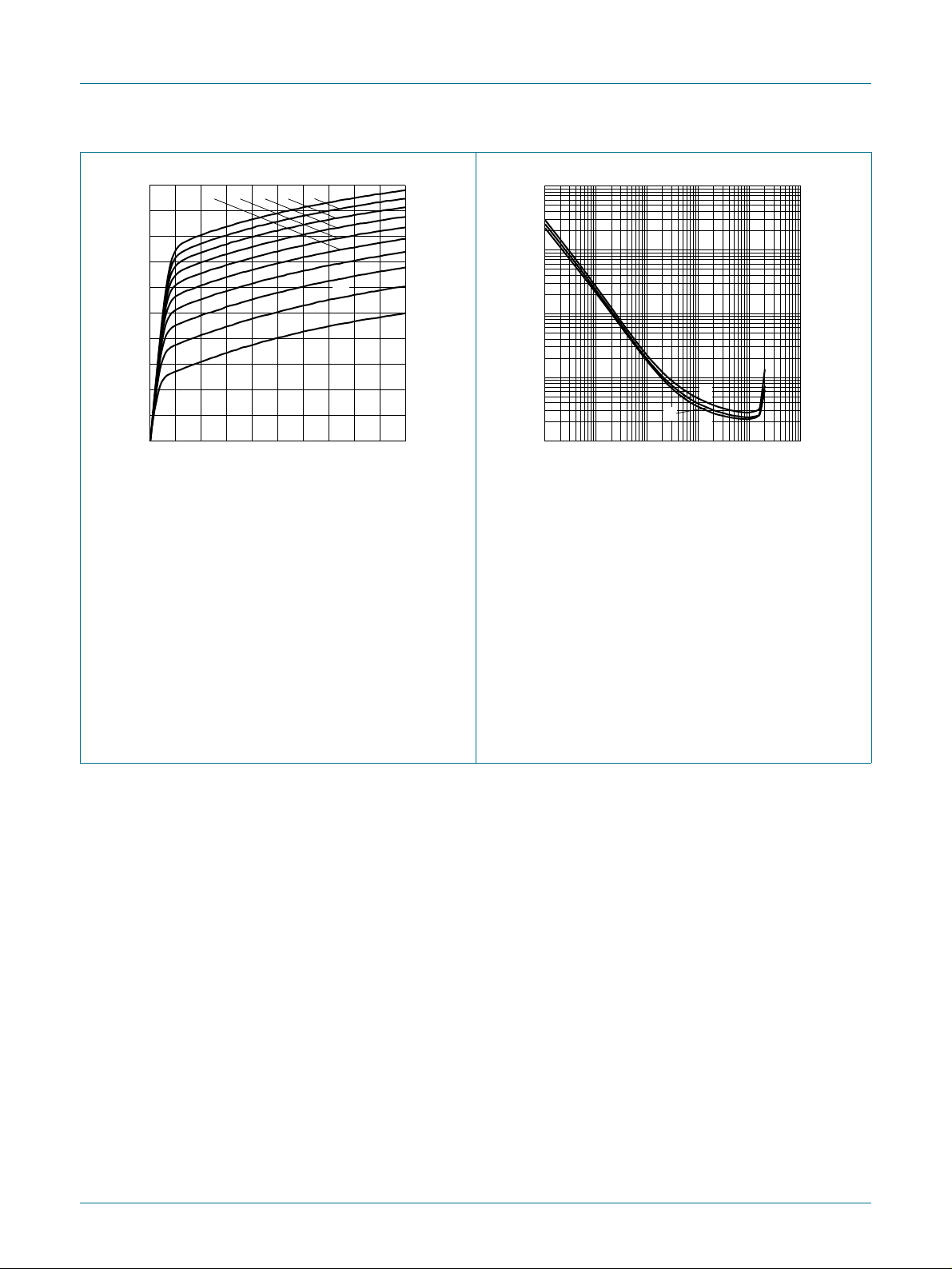
2
I
C
(A)
1.6
1.2
0.8
0.4
0
05
T
(1) I
(2) I
(3) I
(4) I
(5) I
(6) I
(7) I
(8) I
(9) I
(10) I
=25°C
amb
=60mA
B
=54mA
B
=48mA
B
=42mA
B
=36mA
B
=30mA
B
=24mA
B
=18mA
B
=12mA
B
=6mA
B
1
234
(2)(3)(4)(5)(6)
(1)
(7)
(8)
(9)
(10)
V
Fig 9. Collector current as a function of
collector-emitter voltage; typical values
mle131
CE
(V)
R
60 V, 1 A NPN low V
3
10
CEsat
(Ω)
2
10
10
1
−1
10
−1
C/IB
amb
amb
amb
1
=20
= 100 °C
= 25 °C
= −55 °C
10
I
(1) T
(2) T
(3) T
(2)
10 10
(BISS) transistor
CEsat
mle132
(1)
(3)
2
3
10
(mA)
I
C
4
10
Fig 10. Equivalent on-resistance as a function of
collector current; typical values
PBSS4160V_3 © NXP B.V. 2009. All rights reserved.
Product data sheet Rev. 03 — 11 December 2009 8 of 14
Page 9

NXP Semiconductors
PBSS4160V
90 %
10 %
90 %
60 V, 1 A NPN low V
I
B
input pulse
(idealized waveform)
I
(100 %)
Bon
I
Boff
I
C
output pulse
(idealized waveform)
(BISS) transistor
CEsat
IC (100 %)
10 %
t
t
d
r
t
on
Fig 11. BISS transistor switching time definition
(probe)
450 Ω
V
I
R1
= −25 mA
Boff
VCC = 10 V; IC = 0.5 A; I
oscilloscope
= 25 mA; I
Bon
Fig 12. Test circuit for switching times
R2
t
t
s
t
off
V
R
B
BB
V
CC
R
C
V
o
(probe)
oscilloscope
450 Ω
DUT
mlb826
t
f
006aaa003
PBSS4160V_3 © NXP B.V. 2009. All rights reserved.
Product data sheet Rev. 03 — 11 December 2009 9 of 14
Page 10
NXP Semiconductors
6
PBSS4160V
60 V, 1 A NPN low V
(BISS) transistor
CEsat
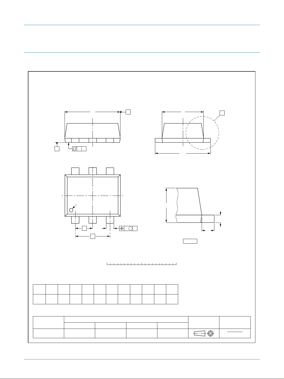
8. Package outline
Plastic surface-mounted package; 6 leads SOT66
D
S
YS
A
E
H
E
X
pin 1 index
123
e
DIMENSIONS (mm are the original dimensions)
UNIT b
mm
A
0.6
0.5
0.27
0.17
p
cD
0.18
0.08
b
1
1.7
1.5
p
e
E
1.3
1.1
456
A
w M
A
0 1 2 mm
scale
e
H
L
1.0
e
1
E
1.7
0.5
1.5
0.3
0.1
p
w
0.1y0.1
detail X
c
L
p
OUTLINE
VERSION
SOT666
REFERENCES
IEC JEDEC JEITA
EUROPEAN
PROJECTION
ISSUE DATE
04-11-08
06-03-16
Fig 13. Package outline SOT666
PBSS4160V_3 © NXP B.V. 2009. All rights reserved.
Product data sheet Rev. 03 — 11 December 2009 10 of 14
Page 11

NXP Semiconductors
PBSS4160V
60 V, 1 A NPN low V
9. Packing information
Table 8. Packing methods
The indicated -xxx are the last three digits of the 12NC ordering code.
Type number Package Description Packing quantity
PBSS4160V SOT666 4 mm pitch, 8 mm tape and reel -1 15
[1] For further information and the availability of packing methods, see Section 12.
[1]
4000
(BISS) transistor
CEsat
PBSS4160V_3 © NXP B.V. 2009. All rights reserved.
Product data sheet Rev. 03 — 11 December 2009 11 of 14
Page 12

NXP Semiconductors
PBSS4160V
60 V, 1 A NPN low V
(BISS) transistor
CEsat
10. Revision history
Table 9. Revision history
Document ID Release date Data sheet status Change notice Supersedes
PBSS4160V_3 20091211 Product data sheet - PBSS4160V_2
Modifications:
PBSS4160V_2 20050131 Product data sheet - PBSS4160V_1
PBSS4160V_1 20040423 Objective data sheet - -
• This data sheet was changed to reflect the new company name NXP Semiconductors,
including new legal definitions and disclaimers. No changes were made to the technical
content.
• Table 2 “Discrete pinning”: updated
• Figure 13 “Package outline SOT666”: updated
PBSS4160V_3 © NXP B.V. 2009. All rights reserved.
Product data sheet Rev. 03 — 11 December 2009 12 of 14
Page 13

NXP Semiconductors
PBSS4160V
60 V, 1 A NPN low V
(BISS) transistor
CEsat
11. Legal information
11.1 Data sheet status
Document status
Objective [short] data sheet Development This document contains data from the objective specification for product development.
Preliminary [short] data sheet Qualification This document contains data from the preliminary specification.
Product [short] data sheet Production This document contains the product specification.
[1] Please consult the most recently issued document before initiating or completing a design.
[2] The term ‘short data sheet’ is explained in section “Definitions”.
[3] The product status of device(s) described in this docu ment may have changed si nce this docum ent was pub lished and may dif fer in case of multiple devices. The latest product status
information is available on the Internet at URL http://www.nxp.com.
11.2 Definitions
Draft — The document is a draft version only. The content is still under
internal review and subject to formal approval, which may result in
modifications or additions. NXP Semiconductors does not give any
representations or warranties as to the accuracy or completeness of
information included herein and shall have no liability for the consequences of
use of such information.
Short data sheet — A short data sheet is an extract from a full data sheet
with the same product type number(s) and title. A short data sheet is intended
for quick reference only and should not be relied u pon to co nt ain det ailed and
full information. For detailed and full information see the relevant full data
sheet, which is available on request via the local NXP Semiconductors sales
office. In case of any inconsistency or conflict with the short data sheet, the
full data sheet shall prevail.
11.3 Disclaimers
General — Information in this document is believed to be accurate and
reliable. However, NXP Semiconduct ors does not give any repr esentatio ns or
warranties, expressed or implied, as to the accuracy or completeness of such
information and shall have no liability for the consequences of use of such
information.
Right to make changes — NXP Semiconductors reserves the right to make
changes to information published in this document, including without
limitation specifications and product descriptions, at any time and without
notice. This document supersedes and replaces all information supplied prior
to the publication hereof.
Suitability for use — NXP Semiconductors products are not designed,
authorized or warranted to be suitable for use in medical, military, aircraft,
space or life support equipment, nor in applications where failure or
malfunction of an NXP Semiconductors product can reasonably be expected
to result in personal injury, death or severe property or environmental
[1][2]
Product status
[3]
Definition
damage. NXP Semiconductors accepts no liability for inclusion and/or use of
NXP Semiconductors products in such equipment or applications and
therefore such inclusion and/or use is at the customer’s own risk.
Applications — Applications that are described herein for any of these
products are for illustrative purposes only. NXP Semiconductors makes no
representation or warranty that such applications will be suitable for the
specified use without further testing or modification.
Limiting values — Stress above one or more limiting values (as defined in
the Absolute Maximum Ratings System of IEC60134) may cause permanent
damage to the device. Limiting values are stress ratings only and operation of
the device at these or any other conditions above those given in the
Characteristics sections of this document is not implied. Exposure to limiting
values for extended periods may affect device reliability.
Terms and conditions of sale — NXP Semiconductors products are sold
subject to the general terms and conditions of commercial sale, as published
at http://www.nxp.com/profile/terms
intellectual property rights infringement and limitation of liability, unless
explicitly otherwise agreed to in writing by NXP Semiconductors. In case of
any inconsistency or conflict between information in this document and such
terms and conditions, the latter will prevail.
No offer to sell or license — Nothing in this document may be interpreted or
construed as an offer to sell product s that is ope n for accept ance or the gr ant,
conveyance or implication of any license under any copyrights, patents or
other industrial or intellectual property rights.
Export control — This document as well as the item(s) described herein
may be subject to export control regulations. Export might require a prior
authorization from national authorities.
Quick reference data — The Quick reference data is an extract of the
product data given in the Limiting values and Characteri stics sections of this
document, and as such is not complete, exhaustive or legally binding.
, including those pertaining to warranty,
11.4 Trademarks
Notice: All referenced brands, product names, service names and trademarks
are the property of their respective owners.
12. Contact information
For more information, please visit: http://www.nxp.com
For sales office addresses, please send an email to: salesaddresses@nxp.com
PBSS4160V_3 © NXP B.V. 2009. All rights reserved.
Product data sheet Rev. 03 — 11 December 2009 13 of 14
Page 14

NXP Semiconductors
PBSS4160V
13. Contents
1 Product profile. . . . . . . . . . . . . . . . . . . . . . . . . . 1
1.1 General description . . . . . . . . . . . . . . . . . . . . . 1
1.2 Features . . . . . . . . . . . . . . . . . . . . . . . . . . . . . . 1
1.3 Applications . . . . . . . . . . . . . . . . . . . . . . . . . . . 1
1.4 Quick reference data . . . . . . . . . . . . . . . . . . . . 1
2 Pinning information. . . . . . . . . . . . . . . . . . . . . . 2
3 Ordering information. . . . . . . . . . . . . . . . . . . . . 2
4 Marking. . . . . . . . . . . . . . . . . . . . . . . . . . . . . . . . 2
5 Limiting values. . . . . . . . . . . . . . . . . . . . . . . . . . 3
6 Thermal characteristics . . . . . . . . . . . . . . . . . . 4
7 Characteristics. . . . . . . . . . . . . . . . . . . . . . . . . . 5
8 Package outline . . . . . . . . . . . . . . . . . . . . . . . . 10
9 Packing information . . . . . . . . . . . . . . . . . . . . 11
10 Revision history. . . . . . . . . . . . . . . . . . . . . . . . 12
11 Legal information. . . . . . . . . . . . . . . . . . . . . . . 13
11.1 Data sheet status . . . . . . . . . . . . . . . . . . . . . . 13
11.2 Definitions. . . . . . . . . . . . . . . . . . . . . . . . . . . . 13
11.3 Disclaimers. . . . . . . . . . . . . . . . . . . . . . . . . . . 13
11.4 Trademarks. . . . . . . . . . . . . . . . . . . . . . . . . . . 13
12 Contact information. . . . . . . . . . . . . . . . . . . . . 13
13 Contents . . . . . . . . . . . . . . . . . . . . . . . . . . . . . . 14
60 V, 1 A NPN low V
(BISS) transistor
CEsat
Please be aware that important notices concerning this document and the product(s)
described herein, have been included in section ‘Legal information’.
© NXP B.V. 2009. All rights reserved.
For more information, please visit: http://www.nxp.com
For sales office addresses, please send an email to: salesaddresses@nxp.com
Date of release: 11 December 2009
Document identifier: PBSS4160V_3
 Loading...