

Page 1

NXP Semiconductors Document identifier: MIMXRT595EVKHUG
User's Guide Rev. 0, 02/2021
MIMXRT595 EVK Board Hardware User's
Guide
Page 2

NXP Semiconductors
Contents
Chapter 1 Introduction........................................................................................... 3
Chapter 2 Getting started.......................................................................................6
Chapter 3 On-board (Link2) debug probe..............................................................8
Chapter 4 Board layout and settings....................................................................10
Chapter 5 Board power........................................................................................20
Chapter 6 Clock sources......................................................................................22
Chapter 7 External memory................................................................................. 23
Chapter 8 On-board peripherals.......................................................................... 26
Chapter 9 Expansion headers............................................................................. 29
Chapter 10 Known issues/errata for revision D................................................... 33
Chapter 11 Revision history.................................................................................34
MIMXRT595 EVK Board Hardware User's Guide, Rev. 0, 02/2021
User's Guide 2 / 35
Page 3

NXP Semiconductors
Chapter 1
Introduction
This document is a Hardware User’s Guide for the MIMXRT595 Evaluation Kit (EVK) based on the NXP Semiconductor i.MX
RT595 Cortex-M33 core processor with Cadence Xtensa Fusion F1 DSP and Vivante GCNanoLite-V vector graphics core. This
board is fully supported by NXP Semiconductor. This Manual includes system setup, debugging information, and provides detailed
information on the overall design and usage of the EVK board from a hardware systems perspective.
1.1 Board overview
This EVK board is a platform designed to showcase many of the most commonly used features of the i.MX RT595 processor in
a small, low-cost package. The MIMXRT595 EVK board is an entry level development board, which gives option to developer
to becoming familiar with the processor before investing a large amount or resources in more specific designs. This document
describes revision D and D1 of the board with B2 silicon (SILICONREV_ID = 0x000B0002).
Features of the MIMXRT595 EVK board are shown below:
• MIMXRT595SFFOC device in 249 FOWLP soldered directly onto the PCB
• Independent voltage domains: VDD_CORE and VDDIO_n’s (0-4)
• 1.2 V, 1.8 V, and 3.3 V support for each voltage domain
• On-board 5 V inputs NXP PCA9420UK PMIC providing 1.2 V, 1.8 V, 3.3 V.
• Multiple power-supply schemes supported
• Jumpers to allow power source selection
• Jumpers for IDD measurement on VDD_CORE and VDDIO_n’s (0-4)
• VBAT coin cell battery holder
• Li-Ion battery header support
• High frequency crystal 24 MHz with compatible footprint
• Low-frequency crystal 32.768 kHz for RTC
• Octal/Quad/pSRAM external memories via FlexSPI
• One reset push button/bootloader selection
• Two push buttons for user input, including Interrupt (SW2) and NMI_b (SW3)
• One motion sensor combo accelero-/magneto-meter NXP FXOS8700CQ
• One RGB LED for user interface
• One Green LED for target MCU power status
• One Red LED for reset status
• One Orange LED for LPC-Link status
• USB2.0 high-speed host and device with micro USB connector and external crystal
• On-board eMMC chip
• Full-size SD card slot
• On-board, high-speed USB, Link2 debug probe with CMSIS-DAP protocol (supports Cortex-M33 debug only) circuit based
on LPC4322 MCU
• Optional external debug probe connections with trace option (10 pin or 20 pin Cortex-M connectors, later required for
trace)
MIMXRT595 EVK Board Hardware User's Guide, Rev. 0, 02/2021
User's Guide 3 / 35
Page 4

NXP Semiconductors
• Single row headers for ARDUINO signals
• MikroBus connector
• FlexIO connector for MikroElektronica TFT Proto 5” capacitive touch display
• Pmod/host expansion connector
• MIPI-DSI connector
• M.2 mini card connector
• Stereo audio codec with line-In/ line-Out/ and Microphone
• NXP TFA9896 audio digital amplifier
• Support for up to 8, off-board digital microphones via 12-pin header
• Two on-board digital microphones
1.2 MIMXRT595 EVK contents
The MIMXRT595 EVK contains the following items:
• MIMXRT595 EVK board
• USB cable (Micro B)
Introduction
• Quick start guide
MIMXRT595 EVK Board Hardware User's Guide, Rev. 0, 02/2021
User's Guide 4 / 35
Page 5
NXP Semiconductors
Introduction
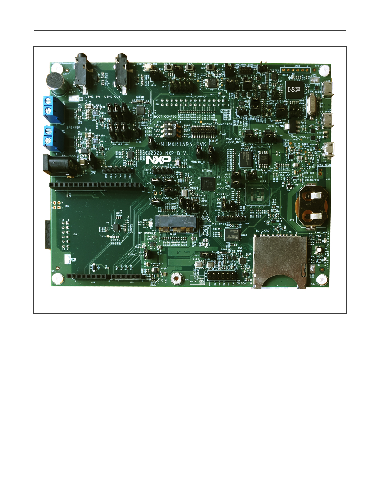
Figure 1. i.MX RT595 board
1.3 MIMXRT595 EVK board revision history
• Rev D
• Rev D1
MIMXRT595 EVK Board Hardware User's Guide, Rev. 0, 02/2021
User's Guide 5 / 35
Page 6

NXP Semiconductors
Chapter 2
Getting started
This section describes how to power up the board and also how to start a first debug session using the MCUXpresso SDK. The
board is pre-programmed with a program indicating that the target MCU is running. Connect a micro USB cable from connector
J40 (LINK USB) to a host computer or supply to power up the board and run this program.
The following debug probes can be used with the board:
• On-board debug probe (LPC4322 Link2), Cortex® M33 only.
• SEGGER J-link probes (version 9 or newer).
Other debug probes may also be supported by IAR and Keil tools and by other IDEs/debug tools. See third-party websites for
further information.
2.1 Starting a debug session using on-board (Link2) Debug Probe
By default, the i.MX RT595 EVK is configured to use the on-board Debug Probe (Link2) via J40 to debug the on-board target (i.MX
RT595), using the CMSIS-DAP debug protocol pre-programmed into the Link2 Flash memory. When connecting the USB cable,
this powers the board and you see that a virtual COM port enumerates.
When using the MCUXpresso IDE, the on-board Link2 can also be booted in the DFU mode (see jumper settings). If this is
done, MCUXpresso IDE downloads CMSIS-DAP to the probe as needed. Using the DFU boot mode, ensure that the most
up-to-date/compatible firmware image is used with MCUXpresso IDE.
The IAR IDE or other development tools that support the CMSIS-DAP protocol can be used in the default configuration (once
support is released for those tools). Check with your toolchain vendor for availability of specific device support packs for the i.MX
RT595 series devices.
NOTE
If the Debug Probe is set up to boot in DFU mode, the USB bridge functions (virtual COM port) and Debug Probe
features will not be available if the board is not first initialized by the MCUXpresso IDE.
2.2 Download and install the MCUXpresso SDK
In order to download the RT500 SDK, visit the MCUXpresso SDK Builder site.
• Go to https://mcuxpresso.nxp.com
• Make sure to log in with NXP account
• Click select development board
• Type in “EVK-MIMXRT595”
• Add desired software components
• Now, download SDK
2.3 Installation steps to use with MCUXpresso IDE
1. Download and install the MCUXpresso IDE v11.3 or latest.
2. Install the RT500 SDK zip package.
3. Install JP1 to force the Link2 Debug Probe to boot in DFU mode.
MIMXRT595 EVK Board Hardware User's Guide, Rev. 0, 02/2021
User's Guide 6 / 35
Page 7

NXP Semiconductors
Getting started
NOTE
If the Debug Probe is set up to boot in DFU mode, the USB bridge functions (virtual COM port) and Debug Probe
features will not be available if the board is not first initialized by the MCUXpresso IDE.
4. Ensure that:
• The jumper JP2 is fitted in position 1-2, local target powered.
• The jumper JP3 is not installed.
5. Connect the board to the USB port of your host computer, connecting a micro USB cable to connector J40 (Link USB).
6. Allow about 10 seconds for the i.MX RT595 EVK device to enumerate for the first time. The device will appear as
LPC-Link2 UCom Port.
Now you can use the MCUXpresso IDE to run the various SDK examples. If the first attempt to debug a project fails in the IDE,
cancel the debug session and repower the board. On some machines the drivers take longer to enumerate for the first time, so
these steps should correct the issue.
2.4 Installation steps to use Keil and IAR tools
1. Download and install LPCScrypt for LPCXpresso boards (http://www.nxp.com/lpcutilities). This installs required drivers
for the board.
NOTE
The Link2 (LPC4322 device) is pre-programmed with CMSIS-DAP firmware during manufacture, so you do not
need to program it.
2. Ensure that JP1 is open to force the Link2 Debug Probe to boot from internal flash.
3. Ensure that jumper JP2 is fitted in position 1-2, and JP3 is not installed. These are the default position set during board
manufacture.
4. Connect the i.MX RT595 board to the USB port of your host computer, connecting a micro USB cable to connector J40
(Link USB). Allow about 10 seconds for the Link2 devices to enumerate for the first time. It is not necessary to check the
Hardware Manager.
Your board is now ready to use with your third-party tool. Follow the instructions for those tools for using a CMSIS-DAP probe.
MCUXpresso IDE can also be used with the board after setting up the board this way.
Now, you can use the Keil/IAR IDE to run the various SDK examples.
NOTE
If using IAR, use v8.50.9 or latest. If using Keil, use v.5.33 or latest.
2.5 Starting a debug session using external Debug Probe
The i.MX RT595 target can also be programmed and debugged using an external Debug Probe that conforms to the standard
Arm® Cortex-M debug connectors (either with 10 pin or 20 pin). To use an external Debug Probe, connect the probe to one of the
SWD connectors (J2 or J19) and connect power via the micro USB connector J39.
MIMXRT595 EVK Board Hardware User's Guide, Rev. 0, 02/2021
User's Guide 7 / 35
Page 8

NXP Semiconductors
Chapter 3
On-board (Link2) debug probe
This section describes the features provided by the on-board Link2 Debug Probe, including how to use this to debug an
external target.
The Link2 Debug Probe is implemented using an LPC43xx MCU, which provides a high-speed USB port interface to the
host computer that runs the development tools. This device is not intended for developer use, and should only be used with
approved firmware images from NXP. The Link2 on-chip flash memory is factory programmed with a firmware image that supports
CMSIS-DAP debug protocol, but also includes other USB end-point functions.
• Virtual COM (VCOM) port: a serial device that can be used with any host computer application design for serial port
communication (for example, Teraterm, puTTY). Set the terminal program for baud rate to 115200, no parity, 8-bit data, 1
stop bit, no flow control.
• SWO trace end point: this virtual device is used by MCUXpresso to retrieve SWO trace data. See the MCUXpresso IDE
documentation for more information.
All of these devices are independent of each other and of the CMSIS-DAP debug device that is enumerated when the board is
connected to a host computer; for example, the VCOM port can be used if the board is running an application when no debugger
is running.
In order to correctly install and use the Link2 device on the i.MX RT595 EVK (required for any debugging purpose) for Windows 7
or 8 host computers, install the drivers first. These drivers will automatically be installed when MCUXpresso IDE has already been
installed. If these IDEs are not being used, it is recommended LPCScrypt be installed as this also includes the required drivers.
All these tools and utilities are available for free download at https://www.nxp.com/lpcscrypt.
The CMSIS-DAP firmware image installed at the factory (and by LPCScrypt) will uniquely identify itself to the host computer so
that more than one board can be connected to that host computer at any time. Some toolchains cannot discern between multiple
debug devices, see your toolchain documentation for more information.
NOTE
MCUXpresso does support multiple LPCXpresso board targets.
It is strongly recommended that LPCScrypt be used to update the Debug Probe firmware in order to ensure that the latest version
is being used.
NOTE
The Link2 only boots when the board is power cycled; the reset button on the board does not reset the Link2.
When using MCUXpresso IDE, the Link2 can be automatically booted with the latest / most appropriate firmware for that IDE
version by installing JP1 DFU jumper before powering up the board. This is the recommended approach for the MCUXpresso IDE.
NOTE
If JP1 is installed when powering the board, then the VCOM port (and other devices mentioned above) device will
not appear until the MCUXpresso IDE boots the Debug Probe. The Debug Probe is booted once a debug session
is started (that is, the IDE attempts to download code to the target).
3.1 Programming the Link2 firmware
As mentioned earlier in this section, it is not normally necessary to program the Link2 firmware. However, this can easily be
accomplished using the supporting utility, LPCScrypt.
To program the Link2 flash, the Link2 device (LPC432x) must be in DFU mode. If the Link2 already has a valid image in the flash, it
needs to be forced into DFU mode by placing a jumper shunt on JP1, and power cycling (disconnecting then reconnecting power).
Link2 MCU programming is performed using the LPCScrypt utility (see http://www.nxp.com/lpcscrypt). Instructions for using the
tool are located at the same webpage. You can also check the instructions in the RT500 Get Started Guide.
MIMXRT595 EVK Board Hardware User's Guide, Rev. 0, 02/2021
User's Guide 8 / 35
Page 9

NXP Semiconductors
On-board (Link2) debug probe
3.2 VCOM port
The identifier of the VCOM port varies between boards and hosts as each board enumerate with a unique identifier. On Windows
OS, to determine the COM port, open the Windows operating system Device Manager. This can be achieved by going to the
Windows operating system click on
“Ports”; the LPC-LinkII UCom Port device and its name should be visible.
This VCOM port will only appear:
• If the Debug Probe has been programmed with the CMSIS-DAP firmware and the Debug Probe DFU link (JP1)
is removed at power-up.
• If the Debug Probe has been configured for DFU boot (JP1) installed at power-up and MCUXpresso IDE has
booted it (by starting a debug session).
Start menu
and typing
Device Manager
NOTE
in the search bar. In the device manager look under
MIMXRT595 EVK Board Hardware User's Guide, Rev. 0, 02/2021
User's Guide 9 / 35
Page 10
NXP Semiconductors
Chapter 4
Board layout and settings
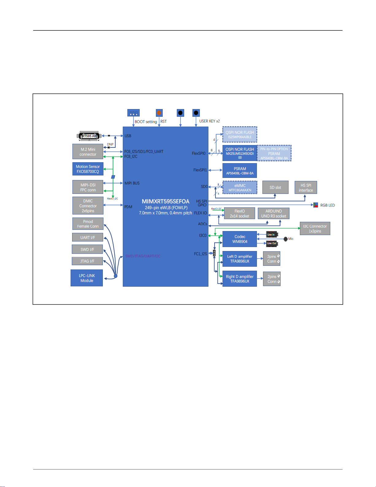
This chapter describes the i.MXRT595-EVK layout, including a description of the jumpers and headers on the board.
Figure 2. i.MX RT595 EVK's block diagram
MIMXRT595 EVK Board Hardware User's Guide, Rev. 0, 02/2021
User's Guide 10 / 35
Page 11
NXP Semiconductors
Board layout and settings
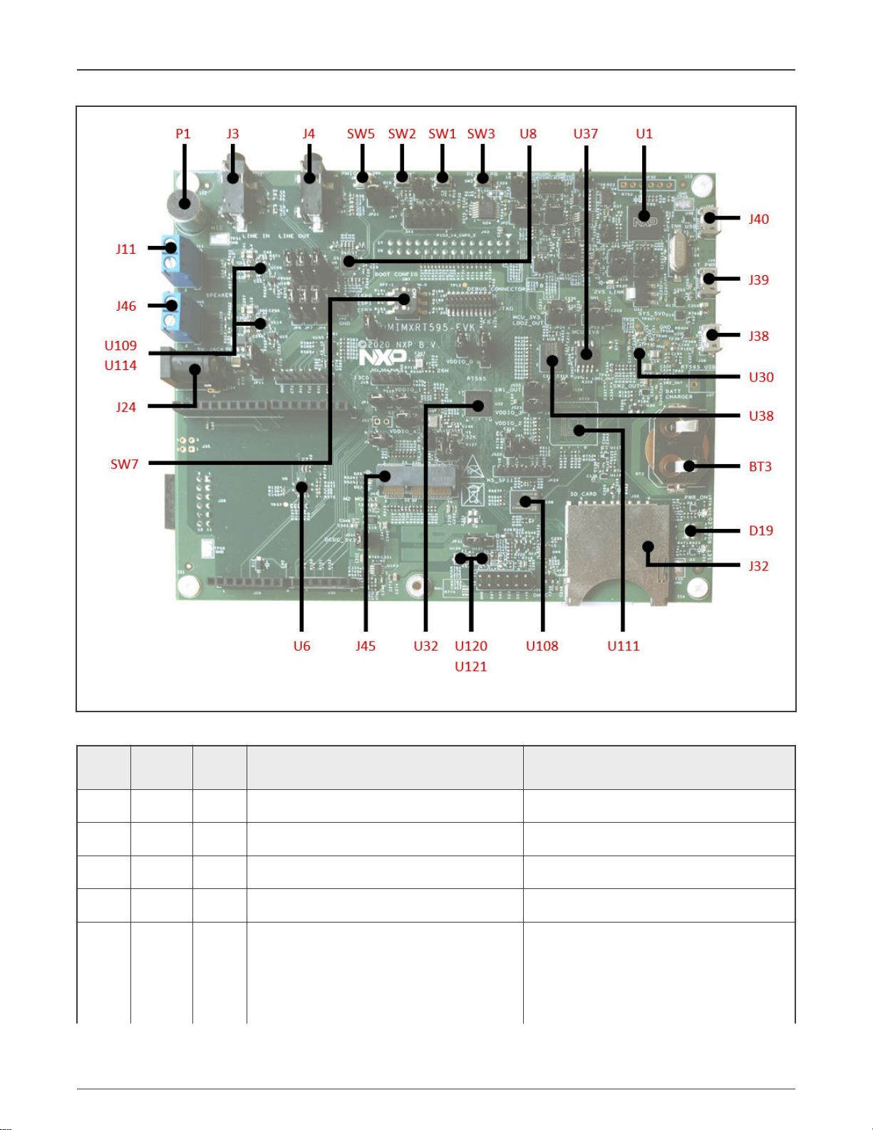
Figure 3. MIMXRT595 EVK board. Components, LEDs, and buttons
Table 1. i.MX RT595 EVK components
Index Circuit
Default Description Reference
Ref.
1 BT3 N/A Coin battery holder. Li-Ion Battery
2 D19 N/A User RGB LED. User LEDs
3 J3 N/A Audio codec line input jack Schematic
4 J4 N/A Audio codec line output jack Schematic
5 J11, J46 N/A Screw terminal connections for external
Schematic
speakers. When attaching a speaker, ensure
that the appropriate driver settings are used
in the TFA9894 devices to avoid damage to
the speaker
Table continues on the next page...
MIMXRT595 EVK Board Hardware User's Guide, Rev. 0, 02/2021
User's Guide 11 / 35
Page 12

NXP Semiconductors
Table 1. i.MX RT595 EVK components (continued)
Board layout and settings
Index Circuit
Default Description Reference
Ref.
6 J24 N/A Additional +5 V power connector. This barrel
Schematic
type connector may be used to supply additional
power to the digital amplifiers, if needed. It
does not power any of the other circuitries on
the board
7 J32 N/A SD Card socket SD Card
8 J38 N/A Micro AB High-speed USB connector
USB High Speed Port
Device/Host
9 J39 N/A External +5 V power. Micro USB connection for
Schematic
power to the i.MX RT595 target and peripheral
circuitry (excluding Link2 Debug Probe)
10 J40 N/A On-board debug probe (LINK USB) micro B
USB connector
Schematic and On-board (PCLink 2)
Debug Probe
11 J45 N/A M.2 connector M.2 Mini Card Connector
12 P1 N/A Microphone Schematic
13 SW1,
SW2
N/A User buttons.
These buttons, when pressed, pulls the
User Buttons
connected i.MX RT595 pin (P0_25 for SW1 and
P0_10 for SW2) to ground. A 100 K ohm pull up
to MCU_1V8 is connected to the pin
14 SW3 N/A Reset button. (Arduino header reset, if JP14
Reset
is installed)
15 SW5 N/A PMIC on button.
Schematic
Press and release to turn on the PMIC. Do not
press down for more than three seconds
16 SW7 SPI0 –
OFF
SPI1 –
OFF
SPI2 –
Boot Config switch.
ISP boot mode selection. Switch the DIP switch
for ISP port signal to ON to pull that pin low via a
1 K ohm resistor. Switch 1 is for ISP0, 2 for ISP1
and 3 for ISP2
Schematic and ISP Boot Config
ON
17 U1 N/A LPC4322 MCU (Link2 device) Schematic
18 U6 N/A FXOS8700CQ Accelerometer/Magnetometer Accelerometer/Magnetometer
19 U8 N/A Audio codec Codec (WM8904)
Table continues on the next page...
MIMXRT595 EVK Board Hardware User's Guide, Rev. 0, 02/2021
User's Guide 12 / 35
Page 13

NXP Semiconductors
Table 1. i.MX RT595 EVK components (continued)
Board layout and settings
Index Circuit
Default Description Reference
Ref.
20 U30 N/A PMIC.
PMIC (PCA9420UK)
Programmable output voltage regulator with
four different outputs: SW1, SW2, LDO1,
and LDO2
21 U32 N/A MIMXRT595 Schematic
22 U37 N/A Quad SPI Flash Octal/Quad Flash
23 U38 N/A Octal SPI Flash Octal/Quad Flash
24 U108 N/A pSRAM pSRAM
25 U109,
N/A Digital Audio Amplifiers Audio Amplifiers
U114
26 U111 N/A eMMC eMMC
27 U120,
N/A On-board DMICs. On-Board DMICs
U121
MIMXRT595 EVK Board Hardware User's Guide, Rev. 0, 02/2021
User's Guide 13 / 35
Page 14

NXP Semiconductors
Board layout and settings
Figure 4. MIMXRT595 EVK (frontside) board jumpers
MIMXRT595 EVK Board Hardware User's Guide, Rev. 0, 02/2021
User's Guide 14 / 35
Page 15

NXP Semiconductors
Board layout and settings
Figure 5. MIMXRT595 EVK (frontside) board jumpers and headers
MIMXRT595 EVK Board Hardware User's Guide, Rev. 0, 02/2021
User's Guide 15 / 35
Page 16

NXP Semiconductors
Board layout and settings
Figure 6. MIMXRT595 EVK (backside) board headers
Table 2. i.MX RT595 EVK expansion headers
Index Circuit Ref. Description Reference
1 J2 10-pin Cortex-M target debug header. Schematic
J18 I3C header Schematic and I3C header
2 J19 Debug Trace Connector. 20-pin Cortex-M debug connector for
Schematic
i.MX RT595 target, including trace pins.
3 J27 - J30 J27, J28, J29, J30 Arduino expansion connectors. Arduino Header
Table continues on the next page...
MIMXRT595 EVK Board Hardware User's Guide, Rev. 0, 02/2021
User's Guide 16 / 35
Page 17

NXP Semiconductors
Table 2. i.MX RT595 EVK expansion headers (continued)
Index Circuit Ref. Description Reference
Board layout and settings
4 J31 External DMIC header.
DMIC daughter card connector
Provides access to all DMIC (PDM) clock and data lines.
5 J36 PMod/Host connector.
PMod connector
This connector provides access to the SPI and I2C ports of
the i.MX RT595 that are also designated for ISP boot. This
connector can be used to work with a remote host, or as
an interface to off-the-shelf PMod expansion boards
J37 Battery Charger Schematic
J43 FLEXIO/LCD Socket FlexIO Socket
J44 MPI/LCD module MIPI-DSI Interface
6 J47 Expansion header Additional expansion Header
7 JP25 USART header USART Header
8 JP26 High-speed SPI header High-speed SPI Header
Table 3. Jumper settings
Index Reference Default Description
1 JS1 1-2 IF_DETECT
2 JP1 OPEN LINK2 ISP BOOT: Link2 (LPC43xx) force DFU boot.
Leave this jumper open (default) for Link2 to follow the normal boot
sequence. The Link2 will boots from internal flash if image is found there.
With the internal flash erased the Link2 normal boot sequence will fall
through to DFU boot.
Install this jumper to force the Link2 to DFU boot mode. Use this setting to
reprogram the Link2 internal flash with a new image (using the LPCScrypt
utility) or to use the MCUXpresso IDE with CMSIS-DAP protocol.
NOTE
Link2 flash is pre-programmed with a version of CMSIS-
DAP firmware by default.
3 JP3 OPEN Target processor selection for the on-board Debug Probe. Jumper open
(default) the i.MX RT595 Target SWD interface enabled. Normal operating
mode where the Target SWD is connected to either the on-board Link2
Debug Probe or an external Debug Probe.
Jumper shunted, the i.MX RT595 Target SWD interface is disabled. Use
this setting only when the on-board Link2 Debug Probe is used to debug an
off-board target MCU.
Table continues on the next page...
MIMXRT595 EVK Board Hardware User's Guide, Rev. 0, 02/2021
User's Guide 17 / 35
Page 18

NXP Semiconductors
Board layout and settings
Table 3. Jumper settings (continued)
Index Reference Default Description
4 JP4 OPEN LINK2 BUFFER for UART and SPI: When open (default), the "Bridge"
UART and SPI connections from the Link2 probe are driven to the i.MX
RT595 target.
Install J10 when using the SPI interface at connector J36 and/or FC0 UART
at J16. This disables the Link2 SPI and UART (VCOM/bridge) connections.
5 JS5 OPEN I2C_SDA: Connects to LPC432x
6 JS6 OPEN I2C_SCL: Connects to LPC432x
7 JS9 1-2 VDD_PMOD: Provides power to PMOD Connector
8 JP14 1-2 UNO_RESET: Reset enable/disable to Arduino. Install jumper to route the
i.MX RT595 reset control signal to the standard Arduino reset pin.
9 JS17 1-2 POR_PULL_UP: Pull-up to PMIC_LDO1_OUT
10 JP17 1-2 LINK2 RST: Reset for the SWD interface
11 JS18 1-2 Buck IC,DCDC_3V3
12 JP18 1-2 SWCLK: SWD port isolation jumpers. When using the VCOM port and an
external debug probe, remove these jumpers to prevent contention with the
on-board debug probe (LPC432x device).
13 JS19 1-2 LDO for LINK2 +2.5V_LINK
14 JP19 1-2 SWDIO SWD port isolation jumpers. When using the VCOM port and an
external debug probe, remove these jumpers to prevent connection with the
on-board debug probe (LPC432x device).
15 JS20 1-2 VDDIO_0: Supply connection to PMIC / external supply injection. This
jumper is provided for optional insertion of an ammeter to measure supply
current to the i.MX RT595 VDDIO_0 supply pins.
16 JS21 1-2 VDDIO_1: Supply connection to PMIC / external supply injection. This
jumper is provided for optional insertion of an ammeter to measure supply
current to the i.MX RT595 VDDIO_1 supply pins.
17 JS22 1-2 VDDIO_2: Supply connection to PMIC / external supply injection. This
jumper is provided for optional insertion of an ammeter to measure supply
current to the i.MX RT595 VDDIO_2 supply pins.
18 JS23 1-2 VDDIO_3: Supply connection to PMIC / external supply injection. This
jumper is provided for optional insertion of an ammeter to measure supply
current to the i.MX RT595 VDDIO_3 supply pins.
19 JS24 1-2 VDDIO_4: Supply connection to PMIC / external supply injection. This
jumper is provided for optional insertion of an ammeter to measure supply
current to the i.MX RT595 VDDIO_4 supply pins.
Table continues on the next page...
MIMXRT595 EVK Board Hardware User's Guide, Rev. 0, 02/2021
User's Guide 18 / 35
Page 19

NXP Semiconductors
Board layout and settings
Table 3. Jumper settings (continued)
Index Reference Default Description
20 JS25 1-2 VDDCORE: Supply connection to PMIC / external supply Injection, the
internal LDO is disabled. This jumper is provided for optional insertion of an
ammeter to measure supply current to the i.MX RT595 VDDCORE supply
pins. If the internal LDO is enabled, this is the output supply.
21 JS26 1-2
Memory 1V8: Isolation jumper for Octal, Quad, and pSRAM memories
22 J41 OPEN GND
23 J42 OPEN GND
24 JP2 1-2
VDD_LINK: Buffer Power Selection
For on-board target place in position 1-2 (default)
For off-board target place in position 2-3
25 JP6 2-3
AMP_INT: Interrupt source select for audio devices, controlling which audio
device drives the interrupt to i.MX RT595.
Insert in position 1-2 for the audio codec or 2-3 for the TFA989x amplifiers
26 JP7 2-3
AMP_DAI: I2S data select for audio devices, controlling which audio device
drives the I2S connections to the i.MX RT595 I2S port. Insert in position
1-2 for the audio codec or 2-3 for the TFA989x amplifiers. Pin is used for
data receive.
27 JP8 2-3
AMP_DAO: I2S data select for audio devices, controlling which audio device
drives the I2S connections to the i.MX RT595 I2S port. Insert in position
1-2 for the audio codec or 2-3 for the TFA989x amplifiers. Pin is used for
data transmit.
28 JP11 1-2 Supply for AMP VBAT,From USB
29 JP13 1-2 ISP_MODE: Host ISP control selection. This header/jumper can be used
to select which of the Port 1 pin 15 (ISP0) or Port 3 pin 28 (ISP1) signals
is routed to the Interrupt/ISP pin on the PMod/Host connector. These
signals from can be used as GPIO/interrupts to/from the i.MX RT595, and
may be used to determine its boot mode following reset.
30 JP21 2-3 Reset signal from PMIC
31 JP23 1-2 MCU_1V8 from PMIC or external LDO
32 JP24 1-2 MCU_3V3 from PMIC or external LDO
33 JP27 2-3 MCLK for codec or AMP
34 JP28 2-3 WS for codec or AMP
35 JP29 2-3 BCLK for codec or AMP
MIMXRT595 EVK Board Hardware User's Guide, Rev. 0, 02/2021
User's Guide 19 / 35
Page 20

NXP Semiconductors
Chapter 5
Board power
The board gets 5 V power from the one of three USB connectors:
• One micro-B connected to the LPC4322 debug probe High-Speed USB port, and which powers the entire board (J40).
• One micro-AB connected to the RT595 High-Speed USB port, and which does not power the debug probe (J38).
• One micro-B for supplying power only to the board (J39).
5.1 Measuring MIMXRT595 EVK device supply current
Current supply to the RT595 Core can be measured via JS25 (VDDCORE). The voltage supplied can be measured on TP42
(SWI1_OUT output voltage from PMIC). GPIO current supplies can be measured via JS20 (VDDIO_0), JS21 (VDDIO_1), JS22
(VDDIO_2), JS23 (VDDIO_3), and JS24 (VDDIO_4). Other headers to measure power are JS29 (VDD_AO) and JS30 (VDD1V8).
For further details, see board schematics.
5.2 PMIC (PCA9420UK)
The MIMXRT595 EVK includes a discrete Power Management Integrated Circuit (PMIC) converter. Using the PMIC adds flexibility
to configure the power supply rails according to the needs of the application. This converter provides all required supplies to all
circuitry except the debug probe. The PMIC has four output voltages, SW1_OUT, SW2_OUT, LDO1_OUT, LDO2_OUT.
Table 4. PMIC output voltages
PMIC output voltage RT500 input voltage Output voltage ranges Default value
SW1_OUT VDDCORE 0.5 – 1.5 V 1.0 V
SW2_OUT VDD1V8
VDDIO_0
VDDIO_1
VDDIO_4
MIPI_DSI_VDD18
LDO1_OUT VDD_AO 1.7 – 1.9 V 1.8 V
LDO2_OUT VDDIO_3
VDDA_BIAS
PMIC is configured by the RT595 via I2C pins:
Table 5. PMIC pins
PMIC iMX RT595
SCL PMIC_I2C_SCL
1.5 – 2.1 V/2.7 V – 3.3 V 1.8 V
1.5 – 2.1 V/2.7 – 3.3 V 3.3 V
SDA PMIC_I2C_SDA
MODESEL0 PMIC_MODE0
Table continues on the next page...
MIMXRT595 EVK Board Hardware User's Guide, Rev. 0, 02/2021
User's Guide 20 / 35
Page 21

NXP Semiconductors
Board power
Table 5. PMIC pins (continued)
PMIC iMX RT595
MODESEL1 PMIC_MODE1
INT PMIC_IRQ_N
SYSRST RESET
ON SW5 (JP21, 1-2)
For further information, see board schematic.
5.3 LDOs
The board design includes 1.8 V and 3.3 V LDOs with 300 mA or more output current capability. Selection between PMIC and the
discrete regulators is to be made using a 3 x 1 header for each rail.
5.4 Li-Ion battery support
The board also includes a header for connecting a Li-Ion battery. The header will not be populated (DNP) by default, and the Li-Ion
battery will not be included with the board or as part of the kit. The connector will allow users to add a battery to be used as the
VBAT power source to the PMIC. The PMIC also includes battery charging capability.
NOTE
When power is supplied from battery, JP31(2-3) must be short. And some functions that belong to 5 V power
domain are limited.
MIMXRT595 EVK Board Hardware User's Guide, Rev. 0, 02/2021
User's Guide 21 / 35
Page 22

NXP Semiconductors
Chapter 6
Clock sources
The RT595 MCU has the capability to run up to 200 MHz. The board includes a 24 MHz crystal as the main external clock source
by default. It also supports an optional 26 MHz crystal.
Additionally, 32.768 kHz external crystal provides a clock source for the RTC.
Clocking sources included on this device are as follows:
• 192 MHz FRO
— Post-divider with 96 MHz, 48 MHz, 24 MHz, 12 MHz outputs.
— Digital feedback control block for frequency tuning.
— 192 MHz output and each of the divided outputs can be individually disabled.
• 96 MHz FRO
— Post-divider with 48 MHz, 24 MHz, 12 MHz, 6 MHz outputs.
— Digital feedback control block for frequency tuning.
— 96 MHz output and each of the divided outputs can be individually disabled.
• Main crystal oscillator with operating range of 4 MHz to 26 MHz.
• 32 kHz Real-Time Clock (RTC) oscillator that can optionally be used as a system clock.
• 1 MHz Low-Power Oscillator (LPOSC).
— LPOSC serves as the watchdog oscillator and clock for the OS/Event Timer and the Systick among others.
— It is also available as the system clock to both domains.
• Separate PLLs for Main Clock, DSP Clock, and Audio (Main clock and DSP clock PLLs are actually 2 PFD outputs from a
single PLL module).
For further information, see Chapter 6. Clock control on the Reference Manual.
MIMXRT595 EVK Board Hardware User's Guide, Rev. 0, 02/2021
User's Guide 22 / 35
Page 23

NXP Semiconductors
Chapter 7
External memory
The board provides various memory options.
7.1 Octal/Quad flash
The board supports a Macronix Octal flash MX25UM51345GXDI00 by default, but the footprint shall accommodate a 1.8 V ISSI
Quad SPI NOR SDR/DDR flash IS25WP064AJBLE as optional on FlexSPI0.
Table 6 shows the hardware modifications needed to use the Octal or Quad flash. Use the schematic for label referral.
Table 6. Octal/Quad SPI hardware modifications
Flash Populated DNP
OctalSPI flash
(MX25UM51345GXDI00)
QuadSPI flash
(IS25WP064AJBLE)
Base on OSPI table, and DNP priority is higher than Populated. If DNP and Populated coexist, choose DNP.
A, B, C, D, E1, E2, F, G, H, M, Q,
S (default)
N, P, Q, S, V1 T, A, C, E1, F, L **
J, K, L, N, P, T, V1 (default)
7.2 pSRAM
An APM APS6408L‐OBx Octal DDR pSRAM memory with compatible footprint is supported on FlexSPI1.
7.3 SD card
A full size SD card slot (J32) in order to accommodate memory SD cards and SDIO Wi-Fi cards. A 4-bit SDIO interface should be
used for this socket on first SDIO instance.
Software drivers and related examples for the SD card are provided as part of the MCUXpresso SDK.
Table 7. SD card connections
SDIO interface signals Circuit reference RT595 port
Clock (CLK) SD0_CLK PIO1_30
Command (CMD) SD0_CMD PIO1_31
D0 SD0_D0 PIO2_0
D1 SD0_D1 PIO2_1
D2 SD0_D2 PIO2_2
D3 SD0_D3 PIO2_3
Card Detect (CD) SD0_CARD_DET_N PIO2_9
Power Enable (WP) SD0_WR_PRT_DS PIO2_4
MIMXRT595 EVK Board Hardware User's Guide, Rev. 0, 02/2021
User's Guide 23 / 35
Page 24

NXP Semiconductors
External memory
NOTE
These signals are shared with the eMMC memory, so hardware changes may be required, depending on your
application. For circuit further details, see board schematics.
7.4 eMMC
An external eMMC memory supporting the SanDisk SDINBDA6-16G-I with 8-bit interface is provided by default. The device can
run at 1.8 V nominal supply voltage.
Software drivers and related examples for the eMMC are provided as part of the MCUXpresso SDK.
Table 8. eMMC connections
eMMC interface signals Circuit reference RT595 Port
Clock (CLK) SD0_CLK PIO1_30
Command (CMD) SD0_CMD PIO1_31
D0 SD0_D0 PIO2_0
D1 SD0_D1 PIO2_1
D2 SD0_D2 PIO2_2
D3 SD0_D3 PIO2_3
D4 SD0_D4 PIO2_5
D5 SD0_D5 PIO2_6
D6 SD0_D6 PIO2_7
D7 SD0_D7 PIO2_8
RESET (RST) SD0_RST_N PIO2_10
DS SD0_WR_PRT_DS PIO2_4
NOTE
These signals are shared with the SD Card slot, so hardware changes may be required depending on your
application. For circuit further details, see board schematics.
7.5 ISP boot config
The ISP pins (PIO1_15, PIO3_28, and PIO3_29) on the boot config SW7, select the boot source:
Table 9. Boot config
Boot mode ISP2 pin
PIO3_29
ISP2 pin
PIO3_29
ISP2 pin
PIO3_29
Description
- low low low Reserved
DFU Master Boot high low high DFU device master serial download boot mode.
Table continues on the next page...
MIMXRT595 EVK Board Hardware User's Guide, Rev. 0, 02/2021
User's Guide 24 / 35
Page 25

NXP Semiconductors
Table 9. Boot config (continued)
External memory
Boot mode ISP2 pin
PIO3_29
ISP2 pin
PIO3_29
ISP2 pin
PIO3_29
Description
USB HID ISP low high low Boot to ISP mode, using USB-HID class.
FlexSPI Boot low high high Boot from Quad/Octal Flash devices connected to
the FLEXSPI interface. The RT500 will look for a
valid image in external Quad/Octal Flash device.
If there is no valid image found, the RT500 will
enter recovery boot or ISP boot mode based on
DEFAULT_ISP_MODE bits.
SDIO0 (eMMC) high low low Boot from an eMMC device connected to SDIO 0
interface. The RT500 will look for a valid image
in the eMMC device. If there is no valid image
found, the RT500 will enter the ISP boot mode
based on the value of OTPDEFAULT_ISP_MODE
bits (6:4, BOOT_CFG[0]).
Serial ISP
(UART, I2C, SPI)
Serial Download (UART,
I2C, SPI, HID)
high high low The Serial Interface (UART, I2C, SPI) is used
to program OTP, external FLASH, SD, or
eMMC device.
high high high Serial Master boot (SPI Slave, or UART, I2C, HID)
is used to download a boot image over the serial
interface(SPI Slave, or UART, I2C, HID).
For further details, See Chapter 18: Non-Secure Boot ROM on the Reference Manual.
MIMXRT595 EVK Board Hardware User's Guide, Rev. 0, 02/2021
User's Guide 25 / 35
Page 26

NXP Semiconductors
Chapter 8
On-board peripherals
This section describes how the on-board peripheral devices of the board are connected to the iMX RT595 and relevant
configuration options. For full details of these devices, refer to the individual device datasheets. For circuit further details, see
board schematics.
8.1 FlexIO socket
There is a 28-pin header (J43) with FlexIO signals connected on the bottom of the board. It is compatible with our third-party
partner, MikroElektronica TFT Proto 5” capacitive touch display, which is supported by the MCUXpresso SDK driver.
8.2 Audio devices
A TFA9896 class D amplifier (stereo configuration) is included on board, using the “easy routing” CSP package. An I2S audio
codec (WM8904), supporting a 1.8 V interface to the RT595 and currently supported by an MCUXpresso SDK driver, is also
included on the board. Jumpers or DIP switches shall be used to select one of these devices (TFA9896 or codec) as an I2S output
channel. The I2S channels (data, SCK, and WS) are connected via zero-ohm resistors to an expansion connector. The (stereo)
line inputs/output of the audio codec are available at jack sockets on the board. Connectors are provided for attaching off-board
speakers to the TFA9896 output.
8.2.1 Codec (WM8904)
The MIMXRT595 EVK board incorporates a Cirrus Logic WM8904 Audio codec. This codec has both I2C (for control) and I2S (for
data) interfaces.
The I2C interface of the codec is routed to Port 2 of the iMX RT595, the same connection as used for the audio amplifiers and the
I3C header on the board; the codec has an address of 0b0011010.
The I2S interface of the codec is routed to Port 0/1 of the iMX RT595, the same connection as used for the audio amplifiers.
Table 10. Audio codec port connections
Circuit reference RT595 port
CODEC_I3C0_SDA P2_30
CODEC_I3C0_SCL P2_29
I2S_BCLK_CODEC P0_7
I2S_DAI_CODEC P0_9
I2S_DAO_CODEC P0_23
I2S_WS_CODEC P0_8
MCLK_CODEC P1_10
ALT_INT_CODEC P0_0
There are six jumpers (JP6, JP7, JP8, JP27, JP28, and JP29) to select iMX RT595 I2S lines between codec and amplifier. To
select the codec, jumpers must be (1-2).
Line input (J3) and line output (J4) ¼” stereo jack sockets provide analog I/O connections to the codec. See schematic for
further information.
MIMXRT595 EVK Board Hardware User's Guide, Rev. 0, 02/2021
User's Guide 26 / 35
Page 27

NXP Semiconductors
On-board peripherals
8.2.2 Audio amplifier
A pair of audio amplifiers are included on the MIMXRT595 EVK. Select the external power supply between JP24 5 V Jack (JP11,
2-3) or J39 USB (JP11, 1-2).
The I2C interface of the amplifiers is routed to Port 2 of the iMX RT595, the same connection as used for the codec and the I3C
header on the board.
The I2S interface of the amplifiers is routed to Port 0/1 of the iMX RT595, the same connection as used for the codec.
Table 11. Digital audio amplifiers port connections
Circuit reference RT595 port
CODEC_I3C0_SDA P2_30
CODEC_I3C0_SCL P2_29
I2S_BCLK_CODEC P0_7
I2S_DAI_CODEC P0_9
I2S_DAO_CODEC P0_23
I2S_WS_CODEC P0_8
MCLK_CODEC P1_10
ALT_INT_CODEC P0_0
There are 6 jumpers (JP6, JP7, JP8, JP27, JP28, and JP29) to select iMX RT595 I2S lines between codec and amplifier. To select
the amplifiers, jumpers must be (2-3).
The connectors provided for attaching off-board speakers to the TFA9896 output are included on the board (J11 and J46). See
schematic for further information.
8.3 USB high-speed port
The board includes a high-speed USB host/device port (J38) connected to the USB signals on the processor. The USB connector
should be micro-AB type.
When the port is used in host mode, the power only USB connector shall be used to provide power to externally connected USB
devices. Jumpers shall be used to configure the USB port for host operation (enabling on-board load switch).
For further details, See High-Speed Device/Host Controller in the Reference Manual.
8.4 MIPI-DSI interface
The board provides a 40-pin FPC connector (J44) to support either MIPI-DSI Video or Smart Displays.
8.5 M.2 Mini card connector
This connector supports the second SDIO instance, UART, I2S, I2C, and USB.
8.6 Accelerometer/magnetometer
The board includes an NXP FXOS8700CQ accelerometer, controlled by I2C interfaced to port 0 (P0_29 and P0_30) with its
interrupt output connected to P0_22. The accelerometer has an I2C address of 0x1E. See schematic for further information.
MIMXRT595 EVK Board Hardware User's Guide, Rev. 0, 02/2021
User's Guide 27 / 35
Page 28

NXP Semiconductors
On-board peripherals
I2C software drivers are provided as part of the MCUXpresso SDK, and example code is provided to illustrate how to read values
from the accelerometer.
8.7 User LEDs
The board provides an RGB LED. The LEDs in this device are controlled by MIMXRT595 ports P3_17 (Blue), P0_14 (Red), P1_0
(Green) with the LEDs being illuminated when the respective LED is pulled low.
8.8 User buttons
The board provides two user push buttons SW1 and SW2 for general input purposes and for wake-up.
8.9 Reset button
A reset button SW3 for the RT595 is provided and resets all devices on the boards except the debug probe.
MIMXRT595 EVK Board Hardware User's Guide, Rev. 0, 02/2021
User's Guide 28 / 35
Page 29

NXP Semiconductors
Chapter 9
Expansion headers
This section describes the various expansion header options and some on-board serial peripherals that are provided on the
MIMXRT595 EVK.
9.1 Arduino header
The connectors J27-J30 provide Arduino compatibility and access to several other signals for use in prototyping.
NOTE
Some ports used on these connectors are shared with other devices/connectors on the board.
The header includes I2C, SPI, UART, GPIOs, and ADC signals.
Table 12. J27 Arduino header pinout
Pin number Circuit reference Functionality
1 FXIO_D11 D0 / UART RX
2 FXIO_D10 D1 / UART TX
3 FXIO_D0 D2 / INT0
4 FXIO_D3 D3 / INT1 / PWM / OC2B
5 FXIO_D4 D4 / T0 / PWM
6 FXIO_D5 D5 / TI / PWM
7 FXIO_D6 D6 / AIN0 / PWM / OC0A
8 FXIO_D7 D7 / AIN1
Table 13. J28 Arduino header pinout
Pin number Circuit reference Functionality
1 FXIO_D8 D8 / CLK0 / ICP1
2 FXIO_D9 D9 / OC1A / PWM
3 FXIO_D12 D10 / SPI_CS
4 FXIO_D13 D11 / OC2A / PWM / SPI_MOSI
5 FXIO_D14 D12 / SPI_MISO
6 FXIO_D15 D13 / SPI_CLK
7 GND
Table continues on the next page...
MIMXRT595 EVK Board Hardware User's Guide, Rev. 0, 02/2021
User's Guide 29 / 35
Page 30

NXP Semiconductors
Table 13. J28 Arduino header pinout (continued)
Pin number Circuit reference Functionality
8 DCDC_3V3 AREF
9 FXIO_D2 D14 / I2C_SDA
10 FXIO_D1 D15 / I2C_SCL
Table 14. J29 Arduino header pinout
Pin number Circuit reference Functionality
1 NC
2 DCDC_3V3 IOREF
3 nRESET_TRGT RESET_b
4 DCDC_3V3 3V3
Expansion headers
5 SYS_5V0 5 V
6 GND GND
7 GND GND
8 SYS_5V0 VIN
Table 15. J30 Arduino header pinout
Pin number Circuit reference Functionality
1 UNO_P0_5_ADC0_0 * A0
2 UNO_P0_6_ADC0_8 * A1
3 UNO_P0_19_ADC0_2 * A2
4 UNO_P0_13_ADC0_9 * A3
5 FXIO_D2 SDA
6 FXIO_D1 SCL
Special Pins. Analog function: 0 V to 1.8 V. Digital function: 0 V or 1.8 V.
NOTE
Arduino shield used should not exceed 200 mA power requirements through 3V3.
9.2 PMod connector
Connector J36 is an optional connector which can provide access for a remote host that support ISP mode. The SPI and I2C serial
ports that support ISP boot shall be available at this connector, along with 2 GPIO/interrupt signals. One of the GPIO signals shall
be ISP0, so an external host can select serial / serial master ISP boot (assuming ISP1 and ISP2 are pulled up internally to RT595).
MIMXRT595 EVK Board Hardware User's Guide, Rev. 0, 02/2021
User's Guide 30 / 35
Page 31

NXP Semiconductors
Table 16. PMod connections
PMOD Pin Circuit Reference RT595 Port
Pin 1 RT_P1_14_SPI_SS0 P1_14
Pin 2 BRIDGE_INTR_ISP P3_28
Pin 3 RT_P1_13_SPI_MOSI P1_13
Pin 4 RT_P0_3_FC0_CTS P0_3
Pin 5 RT_P1_12_SPI_MISO P1_12
Pin 6 RT_P0_15_FC2_SCL P0_15
Pin 7 RT_P1_11_SPI_CLK P1_11
Pin 8 RT_P0_16_FC2_SDA P0_16
Pins 9, 10 GND n/a
Expansion headers
Pins 11, 12 VDD_PMOD VCC_1V8 (JS9)
9.3 I3C header
This header (J18) provides generic access to the I3C interface of the RT595 along with a ground signal. This signals are shared
with the codec and amplifier.
9.4 USART header
Header JP25 is provided as a convenient way to use the USART with a serial to USB cable. Flexcomm 0 ports (P0_1 and P0_2)
are used for this feature, since these ports are assigned for UART ISP mode. These ports are shared with the Link2 debug
probe (LPC4322).
NOTE
When using this header ensure to disable the connection to the Link2. Disconnect JS27 and short JP4.
9.5 High-speed SPI header
Header JP26 provides generic access to the high-speed SPI interface of the RT595 along with a ground signal.
9.6 Additional expansion header
Table 17 shows the pinout for the additional 10-pin header J47.
Table 17. J47 Header pinout
Header pin RT595 port
Pin 1 DCDC_3V3
Pin 2 GND
Pin 3 NC
Table continues on the next page...
MIMXRT595 EVK Board Hardware User's Guide, Rev. 0, 02/2021
User's Guide 31 / 35
Page 32

NXP Semiconductors
Table 17. J47 Header pinout (continued)
Header pin RT595 port
Pin 4 PIO4_5
Pin 5 PIO4_1
Pin 6 PIO4_6
Pin 7 PIO4_3
Pin 8 PIO0_11
Pin 9 PIO3_14
Pin 10 PIO2_15
9.7 DMIC
MIMXRT595 EVK provides two DMIC interfaces described below.
Expansion headers
9.7.1 On-board DMIC
The board incorporates a couple of DMICs on the board. Both DMICs share the data (PIO5_8) and clock (PIO5_4) signals and
are directly routed the RT595.
NOTE
These pins are shared with the External DMIC. By default, on-board DMICS are selected (see R782). For further
details, see board schematics.
9.7.2 DMIC daughter card connector
The board includes a 5x2 0.1” header with connection to the PDM DMIC interfaces of the RT595, for support of the 8 DMIC
daughter board. 2 PDM microphones will be driven in pairs, one sampling data on each edge of the clock signal; therefore 4 clock,
4 data, one ground, and one power signal are required.
Table 18. External DMIC connections
Circuit reference RT595 port
DMIC_PDM_CLK01 PIO5_4
DMIC_PDM_DAT01 PIO5_8
DMIC_PDM_DAT23 PIO3_1
DMIC_PDM_DAT45 PIO3_2
DMIC_PDM_DAT67 PIO3_3
MIMXRT595 EVK Board Hardware User's Guide, Rev. 0, 02/2021
User's Guide 32 / 35
Page 33

NXP Semiconductors
Chapter 10
Known issues/errata for revision D
• Change R547, R548 with RES 12 K from 4.7 K.
• Update layout for DMICs:
— Microphones U120 and U121 to be placed 66 cm apart.
— Acoustic holes should face to the top and not to the bottom.
MIMXRT595 EVK Board Hardware User's Guide, Rev. 0, 02/2021
User's Guide 33 / 35
Page 34

NXP Semiconductors
Chapter 11
Revision history
Table 19 summarizes the changes made to this document since the initial release.
Table 19. Revision history
Revision number Date Substantive changes
0 02/2021 Initial release
MIMXRT595 EVK Board Hardware User's Guide, Rev. 0, 02/2021
User's Guide 34 / 35
Page 35

How To Reach Us
Home Page:
nxp.com
Web Support:
nxp.com/support
Information in this document is provided solely to enable system and software implementers to use NXP
products. There are no express or implied copyright licenses granted hereunder to design or fabricate any
integrated circuits based on the information in this document. NXP reserves the right to make changes without
further notice to any products herein.
NXP makes no warranty, representation, or guarantee regarding the suitability of its products for any particular
purpose, nor does NXP assume any liability arising out of the application or use of any product or circuit,
and specifically disclaims any and all liability, including without limitation consequential or incidental damages.
“Typical” parameters that may be provided in NXP data sheets and/or specifications can and do vary in different
applications, and actual performance may vary over time. All operating parameters, including “typicals,” must
be validated for each customer application by customer's technical experts. NXP does not convey any license
under its patent rights nor the rights of others. NXP sells products pursuant to standard terms and conditions of
sale, which can be found at the following address: nxp.com/SalesTermsandConditions.
Security — Customer understands that all NXP products may be subject to unidentified or documented
vulnerabilities. Customer is responsible for the design and operation of its applications and products throughout
their lifecycles to reduce the effect of these vulnerabilities on customer’s applications and products. Customer’s
responsibility also extends to other open and/or proprietary technologies supported by NXP products for use in
customer’s applications. NXP accepts no liability for any vulnerability. Customer should regularly check security
updates from NXP and follow up appropriately. Customer shall select products with security features that best
meet rules, regulations, and standards of the intended application and make the ultimate design decisions
regarding its products and is solely responsible for compliance with all legal, regulatory, and security related
requirements concerning its products, regardless of any information or support that may be provided by NXP.
NXP has a Product Security Incident Response Team (PSIRT) (reachable at PSIRT@nxp.com) that manages
the investigation, reporting, and solution release to security vulnerabilities of NXP products.
NXP, the NXP logo, NXP SECURE CONNECTIONS FOR A SMARTER WORLD, COOLFLUX, EMBRACE,
GREENCHIP, HITAG, ICODE, JCOP, LIFE, VIBES, MIFARE, MIFARE CLASSIC, MIFARE DESFire, MIFARE
PLUS, MIFARE FLEX, MANTIS, MIFARE ULTRALIGHT, MIFARE4MOBILE, MIGLO, NTAG, ROADLINK,
SMARTLX, SMARTMX, STARPLUG, TOPFET, TRENCHMOS, UCODE, Freescale, the Freescale logo,
AltiVec, CodeWarrior, ColdFire, ColdFire+, the Energy Efficient Solutions logo, Kinetis, Layerscape, MagniV,
mobileGT, PEG, PowerQUICC, Processor Expert, QorIQ, QorIQ Qonverge, SafeAssure, the SafeAssure logo,
StarCore, Symphony, VortiQa, Vybrid, Airfast, BeeKit, BeeStack, CoreNet, Flexis, MXC, Platform in a Package,
QUICC Engine, Tower, TurboLink, EdgeScale, EdgeLock, eIQ, and Immersive3D are trademarks of NXP B.V.
All other product or service names are the property of their respective owners. AMBA, Arm, Arm7, Arm7TDMI,
Arm9, Arm11, Artisan, big.LITTLE, Cordio, CoreLink, CoreSight, Cortex, DesignStart, DynamIQ, Jazelle, Keil,
Mali, Mbed, Mbed Enabled, NEON, POP, RealView, SecurCore, Socrates, Thumb, TrustZone, ULINK, ULINK2,
ULINK-ME, ULINK-PLUS, ULINKpro, μVision, Versatile are trademarks or registered trademarks of Arm Limited
(or its subsidiaries) in the US and/or elsewhere. The related technology may be protected by any or all of
patents, copyrights, designs and trade secrets. All rights reserved. Oracle and Java are registered trademarks
of Oracle and/or its affiliates. The Power Architecture and Power.org word marks and the Power and Power.org
logos and related marks are trademarks and service marks licensed by Power.org.
©
NXP B.V. 2021. All rights reserved.
For more information, please visit: http://www.nxp.com
For sales office addresses, please send an email to: salesaddresses@nxp.com
Date of release: 02/2021
Document identifier: MIMXRT595EVKHUG
 Loading...