

SOT457
IP4223CZ6
Dual USB 2.0 integrated ESD protection
Rev. 1 — 17 October 2011 Product data sheet
1. Product profile
1.1 General description
The IP4223CZ6 is designed to protect I/O lines sensitive to capacitive load, such as
USB 2.0, ethernet, Digital Video Interface (DVI) and so on, from damage due to
ElectroSt atic Discharge (ESD). It incorporates four pairs of ultra low capacitance rail-to- rail
ESD protection diodes plus a Zener diode to provide protection to signal and supply
components from ESD voltages up to 8 kV contact discharge. Protection is supply
voltage independent due to the rail-to-rail diodes being connected to the Zener diode.
The device is encapsulated in a small 6-lead SOT457 (SC-74) Surface-Mounted
Device (SMD) plastic package.
1.2 Features and benefits
Pb-free, Restriction of Hazardous Substances (RoHS) compliant and free of halogen
and antimony (Dark Green compliant)
ESD protection up to 8 kV contact discharge; IEC 61000-4-2, level 4 compliant
Four pairs of ultra low input cap acitance (C
diodes
Low voltage clamping due to integrated Zener diode
Small 6-lead TSOP6 (SOT457) SMD package
(I/O-GND)
= 1.5 pF) ESD rail-to-rail protection
1.3 Applications
General-purpose downstream ESD protection for high-frequency analog signal ports
and high-speed serial data transmission ports in:
Cellular phone and Personal Communication System (PCS) mobile handsets
PC/notebook USB 2.0/IEEE1394 ports
DVI
Cordless telephones
Wireless data (WAN/LAN) systems
Mobile Internet Devices (MID)
Portable Media Players (PMP)
High-Definition Multimedia Interface (HDMI)
NXP Semiconductors
132
4
56
018aaa142
1
2
3
6
5
4
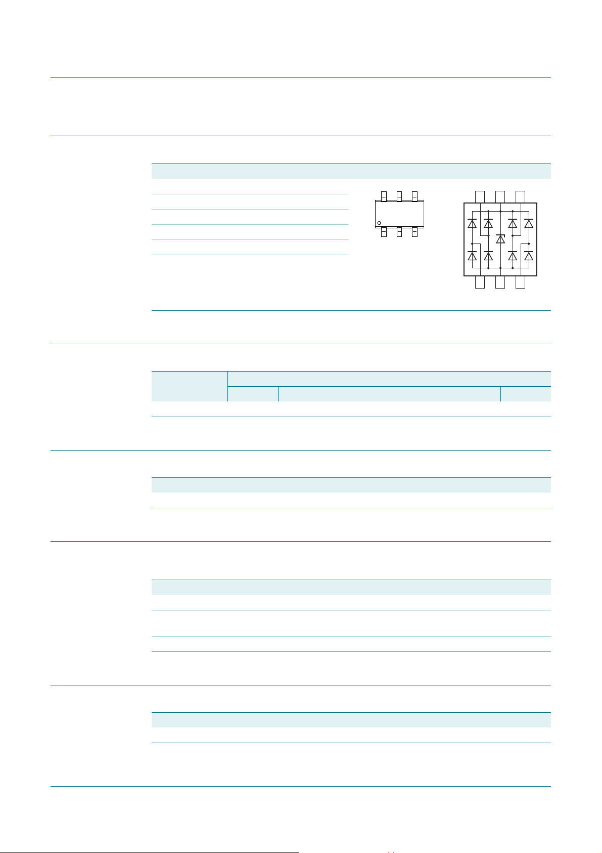
2. Pinning information
Table 1. Pinning
Pin Symbol Description Simplified outline Graphic symbol
1 I/O 1 ESD protection
2 GND ground
3 I/O 2 ESD protection
4 I/O 3 ESD protection
5V
6 I/O 4 ESD protection
3. Ordering information
Table 2. Ordering information
Type number Package
IP4223CZ6 SC-74 plastic surface-mounted package (TSOP6); 6 leads SOT457
IP4223CZ6
Dual USB 2.0 integrated ESD protection
P
supply voltage
Name Description Version
4. Marking
Table 3. Marking codes
Type number Marking code
IP4223CZ6 21
5. Limiting values
Table 4. Limiting values
In accordance with the Absolute Maximum Rating System (IEC 60134).
Symbol Parameter Conditions Min Max Unit
V
I
V
ESD
T
stg
input voltage 0 5.5 V
electrostatic discharge
voltage
IEC 61000-4-2, level 4,
contact; all pins
8+8kV
storage temperature 55 +125 C
6. Recommended operating conditions
Table 5. Operating conditions
Symbol Parameter Conditions Min Typ Max Unit
T
amb
ambient temperature 40 - +85 C
IP4223CZ6 All information provided in this document is subject to legal disclaimers. © NXP B.V. 2011. All rights reserved.
Product data sheet Rev. 1 — 17 October 2011 2 of 9
NXP Semiconductors
018aaa159
4
USB 2.0
IEEE1394
CONTROLLER
5
6
3
2
1
V
BUS
D+
D–
GND
V
BUS
D+
D–
GND
IP4223CZ6
7. Characteristics
Table 6. Characteristics
T
amb
Symbol Parameter Conditions Min Typ Max Unit
C
(I/O-GND)
C
(zd-GND)
I
RM
V
BRzd
V
F
[1] Pins 1, 3, 4 and 6.
[2] Pin 5 to pin 2.
[3] Pins 1, 3, 4 and 6 to ground.
IP4223CZ6
Dual USB 2.0 integrated ESD protection
=25C; unless otherwise specified.
input/output to
ground capacitance
Zener diode to
ground capacitance
VI=0V; f=1MHz;
=3V
V
P
VI=0V; f=1MHz;
VP=3V
reverse leakage current VI=3V
Zener diode breakdown
I=1mA
voltage
forward voltage - 0.7 - V
[1]
--1.5pF
[2]
-40-pF
[3]
- - 100 nA
[2]
6- 9V
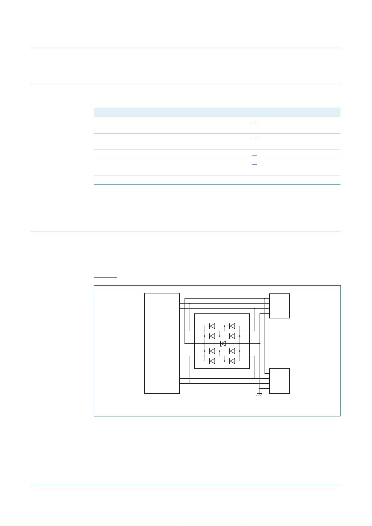
8. Application information
8.1 Universal serial bus 2.0 protection
The device is optimized to protect, for example, two USB 2.0 ports from ESD. Each device
can protect both USB data lines and the V
Figure 1
.
supply line. A typical application is shown in
BUS
Fig 1. Typical application of IP4223CZ6
IP4223CZ6 All information provided in this document is subject to legal disclaimers. © NXP B.V. 2011. All rights reserved.
Product data sheet Rev. 1 — 17 October 2011 3 of 9

NXP Semiconductors
REFERENCES
OUTLINE
VERSION
EUROPEAN
PROJECTION
ISSUE DATE
IEC JEDEC JEITA
SOT457 SC-74
wBM
b
p
D
e
pin 1
index
A
A
1
L
p
Q
detail X
H
E
E
v M
A
AB
y
scale
c
X
132
4
56
0 1 2 mm
Plastic surface-mounted package (TSOP6); 6 leads SOT457
UNIT
A
1
b
p
cD
E
H
E
L
p
Qywv
mm
0.1
0.013
0.40
0.25
3.1
2.7
0.26
0.10
1.7
1.3
e
0.95
3.0
2.5
0.2 0.10.2
DIMENSIONS (mm are the original dimensions)
0.6
0.2
0.33
0.23
A
1.1
0.9
05-11-07
06-03-16
IP4223CZ6
Dual USB 2.0 integrated ESD protection
9. Package outline
Fig 2. Package outline SOT457 (SC-74)
IP4223CZ6 All information provided in this document is subject to legal disclaimers. © NXP B.V. 2011. All rights reserved.
Product data sheet Rev. 1 — 17 October 2011 4 of 9

NXP Semiconductors
solder lands
solder resist
occupied area
solder paste
sot457_fr
3.45
1.95
2.8253.3
0.45
(6×)
0.55
(6×)
0.7
(6×)
0.8
(6×)
2.4
0.95
0.95
Dimensions in mm
sot457_fw
5.3
5.05
1.45
(6×)
0.45
(2×)
1.5
(4×)
2.85
1.475
1.475
solder lands
solder resist
occupied area
preferred transport
direction during soldering
Dimensions in mm
10. Soldering
IP4223CZ6
Dual USB 2.0 integrated ESD protection
Fig 3. Reflow soldering footprint SOT457 (SC-74)
Fig 4. Wave soldering footprint SOT457 (SC-74)
IP4223CZ6 All information provided in this document is subject to legal disclaimers. © NXP B.V. 2011. All rights reserved.
Product data sheet Rev. 1 — 17 October 2011 5 of 9

NXP Semiconductors
IP4223CZ6
Dual USB 2.0 integrated ESD protection
11. Revision history
Table 7. Revision history
Document ID Release date Data sheet status Change notice Supersedes
IP4223CZ6 v.1 20111017 Product data sheet - -
IP4223CZ6 All information provided in this document is subject to legal disclaimers. © NXP B.V. 2011. All rights reserved.
Product data sheet Rev. 1 — 17 October 2011 6 of 9

NXP Semiconductors
IP4223CZ6
Dual USB 2.0 integrated ESD protection
12. Legal information
12.1 Data sheet status
Document status
Objective [short] data sheet Development This document contains data from the objective specification for product development.
Preliminary [short] data sheet Qualification This document contains data from the preliminary specification.
Product [short] data sheet Production This document contains the product specification.
[1] Please consult the most recently issued document before initiating or completing a design.
[2] The term ‘short data sheet’ is explained in section “Definitions”.
[3] The product status of device(s) described in this docu ment may have change d since this d ocument was p ublished and may dif fe r in case of multiple devices. The latest product status
information is available on the Internet at URL http://www.nxp.com.
[1][2]
Product status
[3]
Definition
12.2 Definitions
Draft — The document is a draft version only. The content is still under
internal review and subject to formal approval, which may result in
modifications or additions. NXP Semiconductors does not give any
representations or warranties as to the accuracy or completeness of
information included herein and shall have no liability for the consequences of
use of such information.
Short data sheet — A short data sheet is an extract from a full data sheet
with the same product type number(s) and title. A short data sheet is intended
for quick reference only and should not be relied upon to co nt ain det ailed and
full information. For detailed and full information see the relevant full data
sheet, which is available on request via the local NXP Semiconductors sales
office. In case of any inconsistency or conflict with the short data sheet, the
full data sheet shall prevail.
Product specification — The information and data provided in a Product
data sheet shall define the specification of the product as agreed between
NXP Semiconductors and its customer, unless NXP Semiconductors and
customer have explicitly agreed otherwise in writing. In no event however,
shall an agreement be valid in which the NXP Semiconductors product is
deemed to offer functions and qualities beyond those described in the
Product data sheet.
12.3 Disclaimers
Limited warranty and liability — Information in this document is believed to
be accurate and reliable. However, NXP Semiconductors does not give any
representations or warranties, expressed or implied, as to the accuracy or
completeness of such information and shall have no liability for the
consequences of use of such information.
In no event shall NXP Semiconductors be liable for any indirect, incidental,
punitive, special or consequential damages (including - without limitation - lost
profits, lost savings, business interruption, costs related to the removal or
replacement of any products or rework charges) whether or not such
damages are based on tort (including negligence), warranty, breach of
contract or any other legal theory.
Notwithstanding any damages that customer might incur for any reason
whatsoever, NXP Semi conductors’ aggregat e and cumulative liabil ity towards
customer for the products described herein shall be limited in accordance
with the Terms and conditions of commercial sale of NXP Semiconductors.
Right to make changes — NXP Semiconductors reserves the right to make
changes to information published in this document, including without
limitation specifications and product descriptions, at any time and without
notice. This document supersedes and replaces all information supplied prior
to the publication hereof.
Suitability for use — NXP Semiconductors products are not designed,
authorized or warranted to be suitable for use in life support, life-critical or
safety-critical systems or equipment, nor in applications where failure or
malfunction of an NXP Semiconductors product can reasonably be expected
to result in personal injury, death or severe property or environmental
damage. NXP Semiconductors accepts no liability for inclusion and/or use of
NXP Semiconductors products in such equipment or applications and
therefore such inclusion and/or use is at the customer’s own risk.
Applications — Applications that are described herein for any of these
products are for illustrative purposes only. NXP Semiconductors makes no
representation or warranty that such applications will be suitable for the
specified use without further testing or modification.
Customers are responsible for the design and operation of their applications
and products using NXP Semiconductors products, and NXP Semiconductors
accepts no liability for any assistance with applications or customer product
design. It is customer’s sole responsibility to determine whether the NXP
Semiconductors product is suitable and fit for the customer’s applications and
products planned, as well as for the planned application and use of
customer’s third party customer(s). Customers should provide appropriate
design and operating safeguards to minimize the risks associated with their
applications and products.
NXP Semiconductors does not accept any liability related to any default ,
damage, costs or problem which is based on any weakness or default in the
customer’s applications or products, or the application or use by customer’s
third party customer(s). Customer is responsible for doing all necessary
testing for the customer’s applications and products using NXP
Semiconductors products in order to avoid a default of the applications and
the products or of the application or use by customer’s third part y
customer(s). NXP does not accept any liability in this respect.
Limiting values — Stress above one or more limiting values (as defined in
the Absolute Maximum Ratings System of IEC 60134) will cause permanent
damage to the device. Limiting values are stress ratings only and (proper)
operation of the device at these or any other conditions above those given in
the Recommended operating conditions section (if present) or the
Characteristics sections of this document is not warranted. Constant or
repeated exposure to limiting values will permanently and irreversibly affect
the quality and reliability of the device.
Terms and conditions of commercial sale — NXP Semiconductors
products are sold subject to the general terms and conditions of commercial
sale, as published at http://www.nxp.com/profile/terms
agreed in a valid written individual agreement. In case an individual
agreement is concluded only the terms and conditions of the respective
agreement shall apply. NXP Semiconductors hereby expressly objects to
applying the customer’s general terms and conditions with regard to the
purchase of NXP Semiconductors products by customer.
No offer to sell or license — Nothing in this document may be interpreted or
construed as an offer to sell product s that is open for accept ance or the gr ant,
conveyance or implication of any license under any copyrights, patents or
other industrial or intellectual property rights.
Export control — This document as well as the item(s) described herein
may be subject to export control regulations. Export might require a prior
authorization from competent authorities.
, unless otherwise
IP4223CZ6 All information provided in this document is subject to legal disclaimers. © NXP B.V. 2011. All rights reserved.
Product data sheet Rev. 1 — 17 October 2011 7 of 9

NXP Semiconductors
IP4223CZ6
Dual USB 2.0 integrated ESD protection
Quick reference data — The Quick reference data is an extract of the
product data given in the Limiting values and Characteristics sections of this
document, and as such is not complete, exhaustive or legally binding.
Non-automotive qualified products — Unless this data sheet expressly
states that this specific NXP Semiconductors product is automotive qualified,
the product is not suitable for automotive use. It i s neit her qua lif ied nor tested
in accordance with automotive testing or application requirements. NXP
Semiconductors accepts no liability for inclusion and/or use of
non-automotive qualified products in automotive equipment or applications.
In the event that customer uses the product for design-in and use in
automotive applications to automotive specifications and standards, custome r
(a) shall use the product without NXP Semiconductors’ warranty of the
product for such automotive applications, use and specifications, and (b)
whenever customer uses the product for automotive applications beyond
NXP Semiconductors’ specifications such use shall be solely at customer’s
own risk, and (c) customer fully indemnifies NXP Semiconductors for any
liability, da mages or failed produ ct claims result ing from custome r design and
use of the product for automotive applications beyond NXP Semiconductors’
standard warranty and NXP Semiconductors’ product specifications.
12.4 Trademarks
Notice: All referenced brands, prod uct names, service names and trademarks
are the property of their respective owners.
13. Contact information
For more information, please visit: http://www.nxp.com
For sales office addresses, please send an email to: salesaddresses@nxp.com
IP4223CZ6 All information provided in this document is subject to legal disclaimers. © NXP B.V. 2011. All rights reserved.
Product data sheet Rev. 1 — 17 October 2011 8 of 9

NXP Semiconductors
14. Contents
1 Product profile. . . . . . . . . . . . . . . . . . . . . . . . . . 1
1.1 General description . . . . . . . . . . . . . . . . . . . . . 1
1.2 Features and benefits. . . . . . . . . . . . . . . . . . . . 1
1.3 Applications . . . . . . . . . . . . . . . . . . . . . . . . . . . 1
2 Pinning information. . . . . . . . . . . . . . . . . . . . . . 2
3 Ordering information. . . . . . . . . . . . . . . . . . . . . 2
4 Marking. . . . . . . . . . . . . . . . . . . . . . . . . . . . . . . . 2
5 Limiting values. . . . . . . . . . . . . . . . . . . . . . . . . . 2
6 Recommended operating conditions. . . . . . . . 2
7 Characteristics. . . . . . . . . . . . . . . . . . . . . . . . . . 3
8 Application information. . . . . . . . . . . . . . . . . . . 3
8.1 Universal serial bus 2.0 protection . . . . . . . . . . 3
9 Package outline . . . . . . . . . . . . . . . . . . . . . . . . . 4
10 Soldering . . . . . . . . . . . . . . . . . . . . . . . . . . . . . . 5
11 Revision history. . . . . . . . . . . . . . . . . . . . . . . . . 6
12 Legal information. . . . . . . . . . . . . . . . . . . . . . . . 7
12.1 Data sheet status . . . . . . . . . . . . . . . . . . . . . . . 7
12.2 Definitions. . . . . . . . . . . . . . . . . . . . . . . . . . . . . 7
12.3 Disclaimers. . . . . . . . . . . . . . . . . . . . . . . . . . . . 7
12.4 Trademarks. . . . . . . . . . . . . . . . . . . . . . . . . . . . 8
13 Contact information. . . . . . . . . . . . . . . . . . . . . . 8
14 Contents . . . . . . . . . . . . . . . . . . . . . . . . . . . . . . . 9
IP4223CZ6
Dual USB 2.0 integrated ESD protection
Please be aware that important notices concerning this document and the product(s)
described herein, have been included in section ‘Legal information’.
© NXP B.V. 2011. All rights reserved.
For more information, please visit: http://www.nxp.com
For sales office addresses, please send an email to: salesaddresses@nxp.com
Date of release: 17 October 2011
Document identifier: IP4223CZ6

 Loading...