

2
BZT52H series
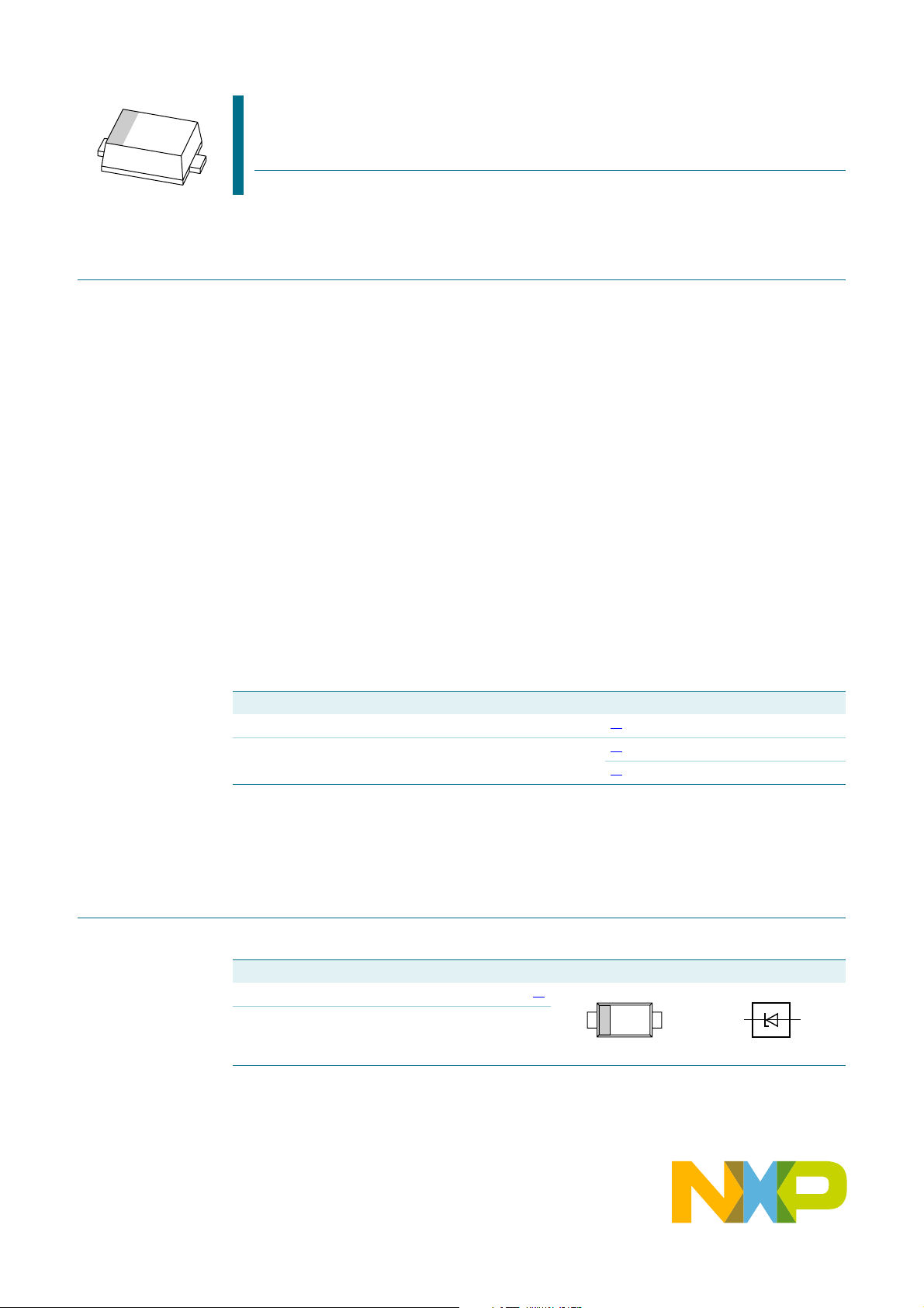
Single Zener diodes in a SOD123F package
Rev. 3 — 7 December 2010 Product data sheet
1. Product profile
1.1 General description
General-purpose Zener diodes in a SOD123F small and flat lead Surface-Mounted
Device (SMD) plastic package.
1.2 Features and benefits
Total power dissipation: ≤ 83 0 mW Low differential resistance
Wide working voltage range: nominal
2.4 V to 75 V (E24 range)
Small plastic package suitable for
surface-mounted design
AEC-Q101 qualified
1.3 Applications
General regulation functions
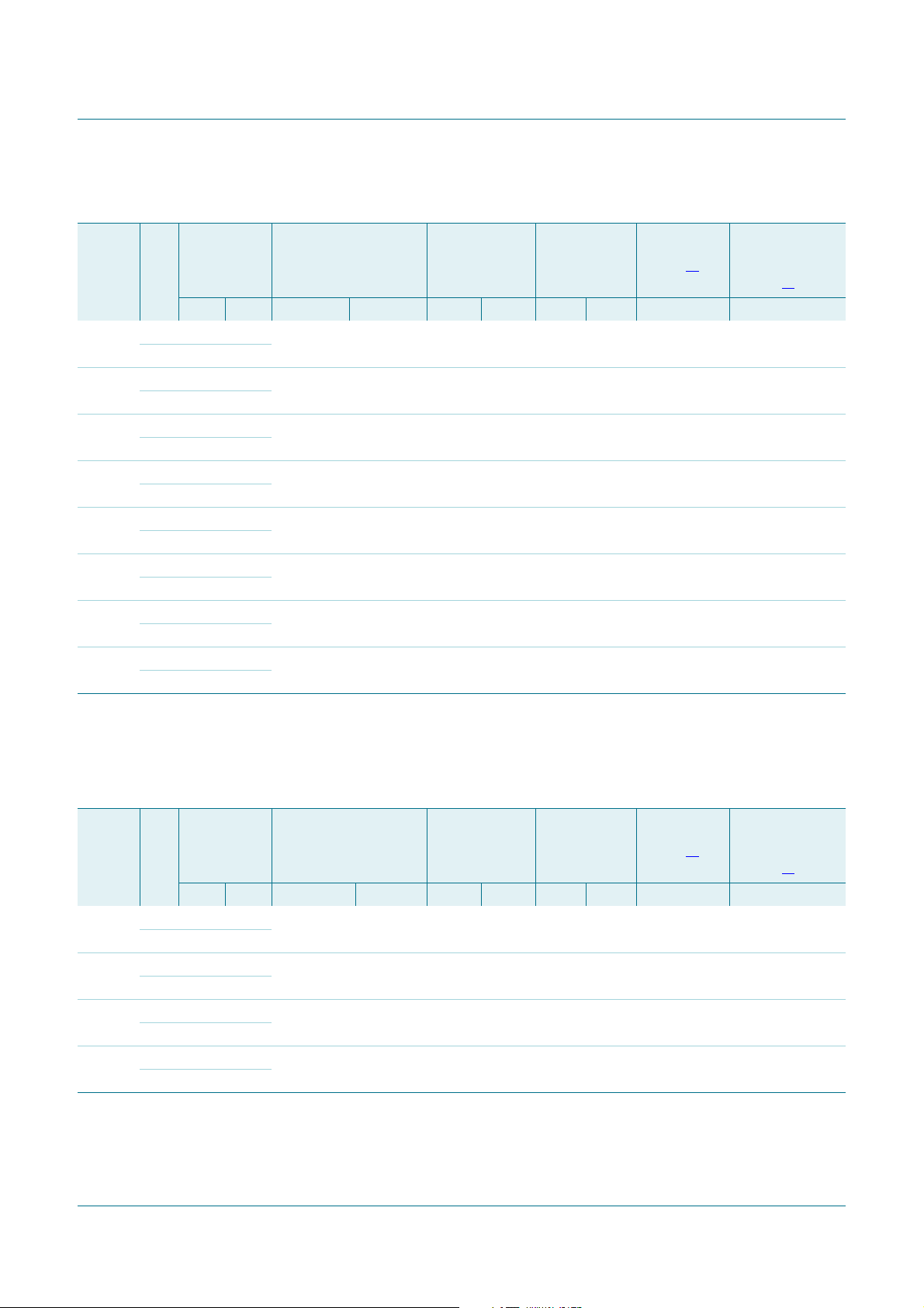
1.4 Quick reference data
Table 1. Quick reference data
Symbol Parameter Conditions Min Typ Max Unit
V
F
P
tot
[1] Pulse test: tp≤ 300μs; δ≤0.02.
[2] Device mounted on an FR4 Printed-Circuit Board (PCB), single-sided copper, tin-plated and standard
[3] Device mounted on an FR4 PCB, single-sided copper, tin-plated, mounting pad for cathode 1 cm2.
forward voltage IF=10mA
total power dissipation T
footprint.
2. Pinning information
Table 2. Pinning
Pin Description Simplified outline Graphic symbol
1 cathode
2 anode
amb
≤ 25 °C
[1]
[1]
--0.9V
[2]
--375mW
[3]
--830mW
21
1
2
006aaa15
[1] The marking bar indicates the cathode.

NXP Semiconductors
3. Ordering information
Table 3. Ordering information
Type number Package
BZT52H-B2V4 to
BZT52H-C75
[1] The series consists of 74 types with nominal working voltages from 2.4 V to 75 V.
[1]
4. Marking
BZT52H series
Single Zener diodes in a SOD123F package
Name Description Version
- plastic surface-mounted package; 2 leads SOD123F
code
Type number Marking
code
Ty pe numb er Marking
code
Type number Marking
code
Table 4. Marking codes
Type number Marking
BZT52H-B2V4 DC BZT52H-B15 DX BZT52H-C2V4 B3 BZT52H-C15 BN
BZT52H-B2V7 DD BZT52H-B16 DY BZT52H-C2V7 B4 BZT52H-C16 BP
BZT52H-B3V0 DE BZT52H-B18 DZ BZT52H-C3V0 B5 BZT52H-C18 BQ
BZT52H-B3V3 DF BZT52H-B20 E1 BZT52H-C3V3 B6 BZT52H-C20 BR
BZT52H-B3V6 DG BZT52H-B22 E2 BZT52H-C3V6 B7 BZT52H-C22 BS
BZT52H-B3V9 DH BZT52H-B24 E3 BZT52H-C3V9 B8 BZT52H-C24 BT
BZT52H-B4V3 DJ BZT52H-B27 E4 BZT52H-C4V3 B9 BZT52H-C27 BU
BZT52H-B4V7 DK BZT52H-B30 E5 BZT52H-C4V7 BA BZT52H-C30 BV
BZT52H-B5V1 DL BZT52H-B33 E6 BZT52H-C5V1 BB BZT52H-C33 BW
BZT52H-B5V6 DM BZT52H-B36 E7 BZT52H-C5V6 BC BZT52H-C36 BX
BZT52H-B6V2 DN BZT52H-B39 E8 BZT52H-C6V2 BD BZT52H-C39 BY
BZT52H-B6V8 DP BZT52H-B43 E9 BZT52H-C6V8 BE BZT52H-C43 BZ
BZT52H-B7V5 DQ BZT52H-B47 EA BZT52H-C7V5 BF BZT52H-C47 C1
BZT52H-B8V2 DR BZT52H-B51 EB BZT52H-C8V2 BG BZT52H-C51 C2
BZT52H-B9V1 DS BZT52H-B56 EC BZT52H-C9V1 BH BZT52H-C56 C3
BZT52H-B10 DT BZT52H-B62 ED BZT52H-C10 BJ BZT52H-C62 C4
BZT52H-B11 DU BZT52H-B68 EE BZT52H-C11 BK BZT52H-C68 C5
BZT52H-B12 DV BZT52H-B75 EF BZT52H-C12 BL BZT52H-C75 C6
BZT52H-B13 DW - - BZT52H-C13 BM - -
BZT52H_SER All information provided in this document is subject to legal disclaimers. © NXP B.V. 2010. All rights reserved.
Product data sheet Rev. 3 — 7 December 2010 2 of 13
NXP Semiconductors
5. Limiting values
Table 5. Limiting values
In accordance with the Absolute Maximum Rating System (IEC 60134).
Symbol Parameter Conditions Min Max Unit
I
F
I
ZSM
P
ZSM
P
tot
T
j
T
amb
T
stg
[1] tp=100μs; square wave; Tj=25°C prior to surge.
[2] Device mounted on an FR4 PCB, single-sided copper, tin-plated and standard footprint.
[3] Device mounted on an FR4 PCB, single-sided copper, tin-plated, mounting pad for cathode 1 cm2.
BZT52H series
Single Zener diodes in a SOD123F package
forward current - 250 mA
non-repetitive peak
reverse current
non-repetitive peak
reverse power dissipation
total power dissipation T
amb
≤ 25 °C
junction temperature - 150 °C
ambient temperature −65 +150 °C
storage temperature −65 +150 °C
- see
Table 8, 9
10
and
[1]
-40W
[2]
- 375 mW
[3]
- 830 mW
6. Thermal characteristics
Table 6. Thermal characteristics
Symbol Parameter Conditions Min Typ Max Unit
R
th(j-a)
R
th(j-sp)
[1] Device mounted on an FR4 PCB, single-sided copper, tin-plated and standard footprint.
[2] Device mounted on an FR4 PCB, single-sided copper, tin-plated, mounting pad for cathode 1 cm2.
[3] Soldering point of cathode tab.
thermal resistance from
junction to ambient
thermal resistance from
junction to solder point
in free air
[1]
--330K/W
[2]
--150K/W
[3]
--70K/W
BZT52H_SER All information provided in this document is subject to legal disclaimers. © NXP B.V. 2010. All rights reserved.
Product data sheet Rev. 3 — 7 December 2010 3 of 13
NXP Semiconductors
7. Characteristics
Table 7. Ch aracteristics
Tj=25°C unless otherwise specified.
Symbol Parameter Conditions Min Typ Max Unit
V
F
[1] Pulse test: tp≤ 300 μs; δ≤0.02.
forward voltage IF=10mA
BZT52H series
Single Zener diodes in a SOD123F package
[1]
--0.9V
Table 8. Characteristics per type; BZT52H-B2V4 to BZT52H-C24
Tj=25°C unless otherwise specified.
BZT52H
-xxx
Sel Working
voltage
(V);
V
Z
IZ=5mA
Maximum differential
resistance r
dif
(Ω)
Reverse
current IR(μA)
Temperature
coefficient
(mV/K);
S
Z
IZ=5mA
Diode
capacitance
[1]
(pF)
C
d
Non-repetitive
peak reverse
current
I
Min Max IZ=1mA IZ=5mA Max VR(V) Min Max Max Max
2V4 B 2.35 2.45 400 85 50 1 −3.5 0.0 450 6.0
C2.22.6
2V7 B 2.65 2.75 500 83 20 1 −3.5 0.0 450 6.0
C2.52.9
3V0 B 2.94 3.06 500 95 10 1 −3.5 0.0 450 6.0
C2.83.2
3V3 B 3.23 3.37 500 95 5 1 −3.5 0.0 450 6.0
C3.13.5
3V6 B 3.53 3.67 500 95 5 1 −3.5 0.0 450 6.0
C3.43.8
3V9 B 3.82 3.98 500 95 3 1 −3.5 0.0 450 6.0
C3.74.1
4V3 B 4.21 4.39 500 95 3 1 −3.5 0.0 450 6.0
C4.04.6
4V7 B 4.61 4.79 500 78 3 2 −3.5 0.2 300 6.0
C4.45.0
5V1 B 5.0 5.2 480 60 2 2 −2.7 1.2 300 6.0
C4.85.4
5V6 B 5.49 5.71 400 40 1 2 −2.0 2.5 300 6.0
C5.26.0
6V2 B 6.08 6.32 150 10 3 4 0.4 3.7 200 6.0
C5.86.6
6V8 B 6.66 6.94 80 8 2 4 1.2 4.5 200 6.0
C6.47.2
7V5 B 7.35 7.65 80 10 1 5 2.5 5.3 150 4.0
C7.07.9
8V2 B 8.04 8.36 80 10 0.7 5 3.2 6.2 150 4.0
C7.78.7
ZSM
(A)
[2]
BZT52H_SER All information provided in this document is subject to legal disclaimers. © NXP B.V. 2010. All rights reserved.
Product data sheet Rev. 3 — 7 December 2010 4 of 13
NXP Semiconductors
BZT52H series
Single Zener diodes in a SOD123F package
Table 8. Characteristics per type; BZT52H-B2V4 to BZT52H-C24
…continued
Tj=25°C unless otherwise specified.
BZT52H
-xxx
Sel Working
voltage
VZ(V);
=5mA
I
Z
Maximum differential
resistance r
dif
(Ω)
Reverse
current IR(μA)
Temperature
coefficient
SZ(mV/K);
=5mA
I
Z
Diode
capacitance
Cd(pF)
[1]
Non-repetitive
peak reverse
current
I
ZSM
Min Max IZ=1mA IZ=5mA Max VR(V) Min Max Max Max
9V1 B 8.92 9.28 100 10 0.5 6 3.8 7.0 150 3.0
C8.59.6
10 B 9.8 10.2 70 10 0.2 7 4.5 8.0 90 3.0
C 9.4 10.6
11 B 10.8 11.2 70 10 0.1 8 5.4 9.0 85 2.5
C 10.4 11.6
12 B 11.8 12.2 90 10 0.1 8 6.0 10.0 85 2.5
C 11.4 12.7
13 B 12.7 13.3 110 10 0.1 8 7.0 11.0 80 2.5
C 12.4 14.1
15 B 14.7 15.3 110 15 0.05 10.5 9.2 13.0 75 2.0
C 13.8 15.6
16 B 15.7 16.3 170 20 0.05 11.2 10.4 14.0 75 1.5
C 15.3 17.1
18 B 17.6 18.4 170 20 0.05 12.6 12.4 16.0 70 1.5
C 16.8 19.1
20 B 19.6 20.4 220 20 0.05 14 14.4 18.0 60 1.5
C 18.8 21.2
22 B 21.6 22.4 220 25 0.05 15.4 16.4 20.0 60 1.25
C 20.8 23.3
24 B 23.5 24.5 220 30 0.05 16.8 18.4 22.0 55 1.25
C 22.8 25.6
(A)
[2]
[1] f = 1 MHz; VR=0V.
= 100 μs; T
[2] t
p
BZT52H_SER All information provided in this document is subject to legal disclaimers. © NXP B.V. 2010. All rights reserved.
Product data sheet Rev. 3 — 7 December 2010 5 of 13
amb
=25°C.
NXP Semiconductors
BZT52H series
Single Zener diodes in a SOD123F package
Table 9. Characteristics per type; BZT52H-B27 to BZT52H-C51
Tj=25°C unless otherwise specified.
BZT52H
-xxx
Sel Working
voltage
(V);
V
Z
IZ=2mA
Maximum differential
resistance r
dif
(Ω)
Reverse
current IR(μA)
Temperature
coefficient
(mV/K);
S
Z
IZ=5mA
Diode
capacitance
[1]
(pF)
C
d
Non-repetitive
peak reverse
current
I
Min Max IZ=1mA IZ=5mA Max VR(V) Min Max Max Max
27 B 26.5 27.5 250 40 0.05 18.9 21.4 25.3 50 1.0
C 25.1 28.9
30 B 29.4 30.6 250 40 0.05 21 24.4 29.4 50 1.0
C 28.0 32.0
33 B 32.3 33.7 250 40 0.05 23.1 27.4 33.4 45 0.9
C 31.0 35.0
36 B 35.3 36.7 250 60 0.05 25.2 30.4 37.4 45 0.8
C 34.0 38.0
39 B 38.2 39.8 300 75 0.05 27.3 33.4 41.2 45 0.7
C 37.0 41.0
43 B 42.1 43.9 325 80 0.05 30.1 37.6 46.6 40 0.6
C 40.0 46.0
47 B 46.1 47.9 325 90 0.05 32.9 42.0 51.8 40 0.5
C 44.0 50.0
51 B 50.0 52.0 350 100 0.05 35.7 46.6 57.2 40 0.4
C 48.0 54.0
ZSM
(A)
[2]
[1] f = 1 MHz; VR=0V.
= 100 μs; T
[2] t
p
Table 10. Characteristics per type; BZT52H-B56 to BZT52H-C75
=25
T
°
C unless otherwise specified.
j
BZT52H
Sel Working
-xxx
=25°C.
amb
voltage
VZ(V);
=2mA
I
Z
Maximum differential
resistance r
dif
(Ω)
Reverse
current IR(μA)
Temperature
coefficient
SZ(mV/K);
=5mA
I
Z
Diode
capacitance
Cd(pF)
[1]
Non-repetitive
peak reverse
current
I
ZSM
Min Max IZ=0.5mA IZ=2mA Max VR(V) Min Max Max Max
56 B 54.9 57.1 375 120 0.05 39.2 52.2 63.8 40 0.3
C 52.0 60.0
62 B 60.8 63.2 400 140 0.05 43.4 58.8 71.6 35 0.3
C 58.0 66.0
68 B 66.6 69.4 400 160 0.05 47.6 65.6 79.8 35 0.25
C 64.0 72.0
75 B 73.5 76.5 400 175 0.05 52.5 73.4 88.6 35 0.20
C 70.0 79.0
[1] f = 1 MHz; VR=0V.
[2] tp= 100 μs; T
amb
=25°C.
(A)
[2]
BZT52H_SER All information provided in this document is subject to legal disclaimers. © NXP B.V. 2010. All rights reserved.
Product data sheet Rev. 3 — 7 December 2010 6 of 13

NXP Semiconductors
BZT52H series
Single Zener diodes in a SOD123F package
tp (ms)
mbg801
10
P
ZSM
(W)
3
10
2
10
10
1
−1
10
(1)
(2)
1
(1) Tj=25°C (prior to surge)
= 150 °C (prior to surge)
(2) T
j
Fig 1. Non-repetitive peak reverse power dissipation
as a function of pulse duration; maximum
values
mbg783
3V9
3V6
3V3
3V0
S
Z
(mV/K)
0
4V3
−1
−2
300
I
F
(mA)
200
100
0
0.6 10.8
mbg781
VF (V)
Tj=25°C
Fig 2. Forward current as a function of forward
voltage; typical values
mbg782
S
Z
(mV/K)
10
12
11
10
5
0
9V1
8V2
7V5
6V8
6V2
5V6
5V1
4V7
2V4
2V7
−3
060
20 40
I
Z
(mA)
BZT52H-B/C2V4 to BZT52H-B/C4V3
=25°C to 150 °C
T
j
Fig 3. Temperature coefficient as a function of
working current; typical values
BZT52H_SER All information provided in this document is subject to legal disclaimers. © NXP B.V. 2010. All rights reserved.
−5
02016
4812
I
Z
(mA)
BZT52H-B/C4V7 to BZT52H-B/C12
Tj=25°C to 150 °C
Fig 4. Temperature coefficient as a function of
working current; typical values
Product data sheet Rev. 3 — 7 December 2010 7 of 13

NXP Semiconductors
8. Test information
8.1 Quality information
This product has been qualified in accordance with the Automotive Electronics Council
(AEC) standard Q101 - Stress test qualification for discrete semiconductors, and is
suitable for use in automotive applications.
9. Package outline
BZT52H series
Single Zener diodes in a SOD123F package
Fig 5. Package outline SOD123F
10. Packing information
Table 11. Packing methods
The indicated -xxx are the last three digits of the 12NC ordering code.
Type number Package Description Packing quantity
BZT52H-B2V4 to
BZT52H-C75
1.2
1.0
0.25
0.10
04-11-29Dimensions in mm
[1]
3.6
3.4
2.7
2.5
1.7
1.5
0.70
0.55
1
0.55
0.35
2
3000 10000
SOD123F 4 mm pitch, 8 mm tape and reel -115 -135
[1] For further information and the availability of packing methods, see Section 14.
BZT52H_SER All information provided in this document is subject to legal disclaimers. © NXP B.V. 2010. All rights reserved.
Product data sheet Rev. 3 — 7 December 2010 8 of 13

NXP Semiconductors
11. Soldering
Fig 6. Reflow soldering footprint SOD123F
Single Zener diodes in a SOD123F package
4.4
4
2.9
1.6
1.6
1.1
(2×)
Reflow soldering is the only recommended soldering method.
Dimensions in mm.
1.1 1.22.1
BZT52H series
solder lands
solder resist
solder paste
occupied area
BZT52H_SER All information provided in this document is subject to legal disclaimers. © NXP B.V. 2010. All rights reserved.
Product data sheet Rev. 3 — 7 December 2010 9 of 13

NXP Semiconductors
BZT52H series
Single Zener diodes in a SOD123F package
12. Revision history
Table 12. Revision history
Document ID Release date Data sheet status Change notice Supersedes
BZT52H_SER v.3 20101207 Product data sheet - BZT52H_SER v.2
Modifications: • Added selection B.
Section 1.2 “Features and benefits”: amended.
•
•
Table 2 “Pinning”: graphic symbol updated.
Section 8 “Test information”: added.
•
Section 13 “Legal information”: updated.
•
BZT52H_SER v.2 20091115 Product data sheet - BZT52H_SER v.1
BZT52H_SER v.1 20051222 Product data sheet - -
BZT52H_SER All information provided in this document is subject to legal disclaimers. © NXP B.V. 2010. All rights reserved.
Product data sheet Rev. 3 — 7 December 2010 10 of 13

NXP Semiconductors
BZT52H series
Single Zener diodes in a SOD123F package
13. Legal information
13.1 Data sheet status
Document status
Objective [short] data sheet Development This document contains data from the objective specification for product development.
Preliminary [short] data sheet Qualification This document contains data from the preliminary specification.
Product [short] data sheet Production This document contains the product specification.
[1] Please consult the most recently issued document before initiating or completing a design.
[2] The term ‘short data sheet’ is explained in section “Definitions”.
[3] The product status of device(s) described in this docu ment may have changed si nce this docum ent was pub lished and may dif fer in case of multiple devices. The latest product statu s
information is available on the Internet at URL
[1][2]
Product status
http://www.nxp.com.
[3]
Definition
13.2 Definitions
Draft — The document is a draft version only. The content is still under
internal review and subject to formal approval, which may result in
modifications or additions. NXP Semiconductors does not give any
representations or warranties as to the accuracy or completeness of
information included herein and shall have no liability for the consequences of
use of such information.
Short data sheet — A short data sheet is an extract from a full data sheet
with the same product type number(s) and title. A short data sheet is intended
for quick reference only and should not be relied u pon to co nt ain det ailed and
full information. For detailed and full information see the relevant full data
sheet, which is available on request via the local NXP Semiconductors sales
office. In case of any inconsistency or conflict with the short data sheet, the
full data sheet shall prevail.
Product specification — The information and data provided in a Product
data sheet shall define the specification of the product as agreed between
NXP Semiconductors and its customer, unless NXP Semiconductors and
customer have explicitly agreed otherwise in writing. In no event however,
shall an agreement be valid in which the NXP Semiconductors product is
deemed to offer functions and qualities beyond those described in the
Product data sheet.
13.3 Disclaimers
Limited warranty and liability — Information in this document is believed to
be accurate and reliable. However, NXP Semiconductors does not give any
representations or warranties, expressed or implied, as to the accuracy or
completeness of such information and shall have no liability for the
consequences of use of such information.
In no event shall NXP Semiconductors be lia ble for any indirect, incidental,
punitive, special or consequential damages (including - without limitation - lost
profits, lost savings, business interruption, costs related to the removal or
replacement of any products or rework charges) whether or not such
damages are based on tort (including negligence), warranty, breach of
contract or any other legal theory.
Notwithstanding any damages that customer might incur for any reason
whatsoever, NXP Semi conductors’ aggregat e and cumulative liabil ity towards
customer for the products described herein shall be limited in accordance
with the Terms and conditions of commercial sale of NXP Semiconductors.
Right to make changes — NXP Semiconductors reserves the right to make
changes to information published in this document, including without
limitation specifications and product descriptions, at any time and without
notice. This document supersedes and replaces all information supplied prior
to the publication hereof.
Suitability for use — NXP Semiconductors products are not designed,
authorized or warranted to be suitable for use in life support, life-critical or
safety-critical systems or equipment, nor in applications where failure or
malfunction of an NXP Semiconductors product can reasonabl y be expected
to result in personal injury, death or severe property or environmental
damage. NXP Semiconductors accepts no liability for inclusion and/or use of
NXP Semiconductors products in such equipment or applications and
therefore such inclusion and/or use is at the customer’s own risk.
Applications — Applications that are described herein for any of these
products are for illustrative purposes only. NXP Semiconductors makes no
representation or warranty that such applications will be suitable for the
specified use without further testing or modification.
Customers are responsible for the design and operation of their applications
and products using NXP Semiconductors products, and NXP Semiconductors
accepts no liability for any assistance with applications or customer product
design. It is customer’s sole responsibility to determine whether the NXP
Semiconductors product is suitable and fit for the customer’s applications and
products planned, as well as for the planned application and use of
customer’s third party customer(s). Customers should provide appropriate
design and operating safeguards to minimize the risks associated with their
applications and products.
NXP Semiconductors does not accept any liability related to any default ,
damage, costs or problem which is based on any weakness or default in the
customer’s applications or products, or the application or use by customer’s
third party customer(s). Customer is responsible for doing all necessary
testing for the customer’s applications and products using NXP
Semiconductors products in order to avoid a default of the applications and
the products or of the application or use by customer’s third part y
customer(s). NXP does not accept any liability in this respect.
Limiting values — Stress above one or more limiting values (as defined in
the Absolute Maximum Ratings System of IEC 60134) will cause permanent
damage to the device. Limiting values are stress ratings only and (proper)
operation of the device at these or any other conditions above those given in
the Recommended operating conditions section (if present) or the
Characteristics sections of this document is not warranted. Constant or
repeated exposure to limiting values will permanently and irreversibly affect
the quality and reliability of the device.
Terms and conditions of commercial sale — NXP Semiconductors
products are sold subject to the general terms and conditions of commercial
sale, as published at
agreed in a valid written individual agreement. In case an individual
agreement is concluded only the terms and conditions of the respective
agreement shall apply. NXP Semiconductors hereby expressly objects to
applying the customer’s general terms and conditions with regard to the
purchase of NXP Semiconductors products by customer.
No offer to sell or license — Nothing in this document may be interpreted or
construed as an offer to sell product s that is ope n for accept ance or the gr ant,
conveyance or implication of any license under any copyrights, patents or
other industrial or intellectual property rights.
Export control — This document as well as the item(s) described herein
may be subject to export control regulations. Export might require a prior
authorization from national authorities.
http://www.nxp.com/profile/terms
, unless otherwise
BZT52H_SER All information provided in this document is subject to legal disclaimers. © NXP B.V. 2010. All rights reserved.
Product data sheet Rev. 3 — 7 December 2010 11 of 13

NXP Semiconductors
BZT52H series
Single Zener diodes in a SOD123F package
Quick reference data — The Quick reference data is an extract of the
product data given in the Limiting values and Characteristics sections of this
document, and as such is not complete, exhaustive or legally binding.
13.4 Trademarks
Notice: All referenced brands, prod uct names, service names and trad emarks
are the property of their respective owners.
14. Contact information
For more information, please visit: http://www.nxp.com
For sales office addresses, please send an email to: salesaddresses@nxp.com
BZT52H_SER All information provided in this document is subject to legal disclaimers. © NXP B.V. 2010. All rights reserved.
Product data sheet Rev. 3 — 7 December 2010 12 of 13

NXP Semiconductors
15. Contents
1 Product profile. . . . . . . . . . . . . . . . . . . . . . . . . . 1
1.1 General description . . . . . . . . . . . . . . . . . . . . . 1
1.2 Features and benefits. . . . . . . . . . . . . . . . . . . . 1
1.3 Applications . . . . . . . . . . . . . . . . . . . . . . . . . . . 1
1.4 Quick reference data . . . . . . . . . . . . . . . . . . . . 1
2 Pinning information. . . . . . . . . . . . . . . . . . . . . . 1
3 Ordering information. . . . . . . . . . . . . . . . . . . . . 2
4 Marking. . . . . . . . . . . . . . . . . . . . . . . . . . . . . . . . 2
5 Limiting values. . . . . . . . . . . . . . . . . . . . . . . . . . 3
6 Thermal characteristics . . . . . . . . . . . . . . . . . . 3
7 Characteristics. . . . . . . . . . . . . . . . . . . . . . . . . . 4
8 Test information. . . . . . . . . . . . . . . . . . . . . . . . . 8
8.1 Quality information . . . . . . . . . . . . . . . . . . . . . . 8
9 Package outline . . . . . . . . . . . . . . . . . . . . . . . . . 8
10 Packing information . . . . . . . . . . . . . . . . . . . . . 8
11 Soldering . . . . . . . . . . . . . . . . . . . . . . . . . . . . . . 9
12 Revision history. . . . . . . . . . . . . . . . . . . . . . . . 10
13 Legal information. . . . . . . . . . . . . . . . . . . . . . . 11
13.1 Data sheet status . . . . . . . . . . . . . . . . . . . . . . 11
13.2 Definitions. . . . . . . . . . . . . . . . . . . . . . . . . . . . 11
13.3 Disclaimers. . . . . . . . . . . . . . . . . . . . . . . . . . . 11
13.4 Trademarks. . . . . . . . . . . . . . . . . . . . . . . . . . . 12
14 Contact information . . . . . . . . . . . . . . . . . . . . . 12
15 Contents. . . . . . . . . . . . . . . . . . . . . . . . . . . . . . 13
BZT52H series
Single Zener diodes in a SOD123F package
Please be aware that important notices concerning this document and the product(s)
described herein, have been included in section ‘Legal information’.
© NXP B.V. 2010. All rights reserved.
For more information, please visit: http://www.nxp.com
For sales office addresses, please send an email to: salesaddresses@nxp.com
Date of release: 7 December 2010
Document identifier: BZT52H_SER

 Loading...