


BFQ591
NPN 7 GHz wideband transistor
Rev. 04 — 2 October 2007 Product data sheet
IMPORTANT NOTICE
Dear customer,
As from October 1st, 2006 Philips Semiconductors has a new trade name
- NXP Semiconductors, which will be used in future data sheets together with new contact
details.
In data sheets where the previous Philips references remain, please use the new links as
shown below.
http://www.philips.semiconductors.com use http://www.nxp.com
http://www.semiconductors.philips.com use http://www.nxp.com (Internet)
sales.addresses@www.semiconductors.philips.com use salesaddresses@nxp.com
(email)
The copyright notice at the bottom of each page (or elsewhere in the document,
depending on the version)
- © Koninklijke Philips Electronics N.V. (year). All rights reserved is replaced with:
- © NXP B.V. (year). All rights reserved. If you have any questions related to the data sheet, please contact our nearest sales
office via e-mail or phone (details via salesaddresses@nxp.com). Thank you for your
cooperation and understanding,
NXP Semiconductors
NXP Semiconductors Product specification
Rev. 04 - 2 October 2007
2 of 11
NPN 7 GHz wideband transistor BFQ591
FEATURES
• High power gain
• Low noise figure
• High transition frequency
• Gold metallization ensures excellent reliability.
APPLICATIONS
Intended for applications intheGHz range such as MATV
or CATV amplifiers and RF communications subscribers
equipment.
DESCRIPTION
NPN wideband transistor in a SOT89 plastic package.
MARKING
TYPE NUMBER MARKING CODE
BFQ591 BCp
QUICK REFERENCE DATA
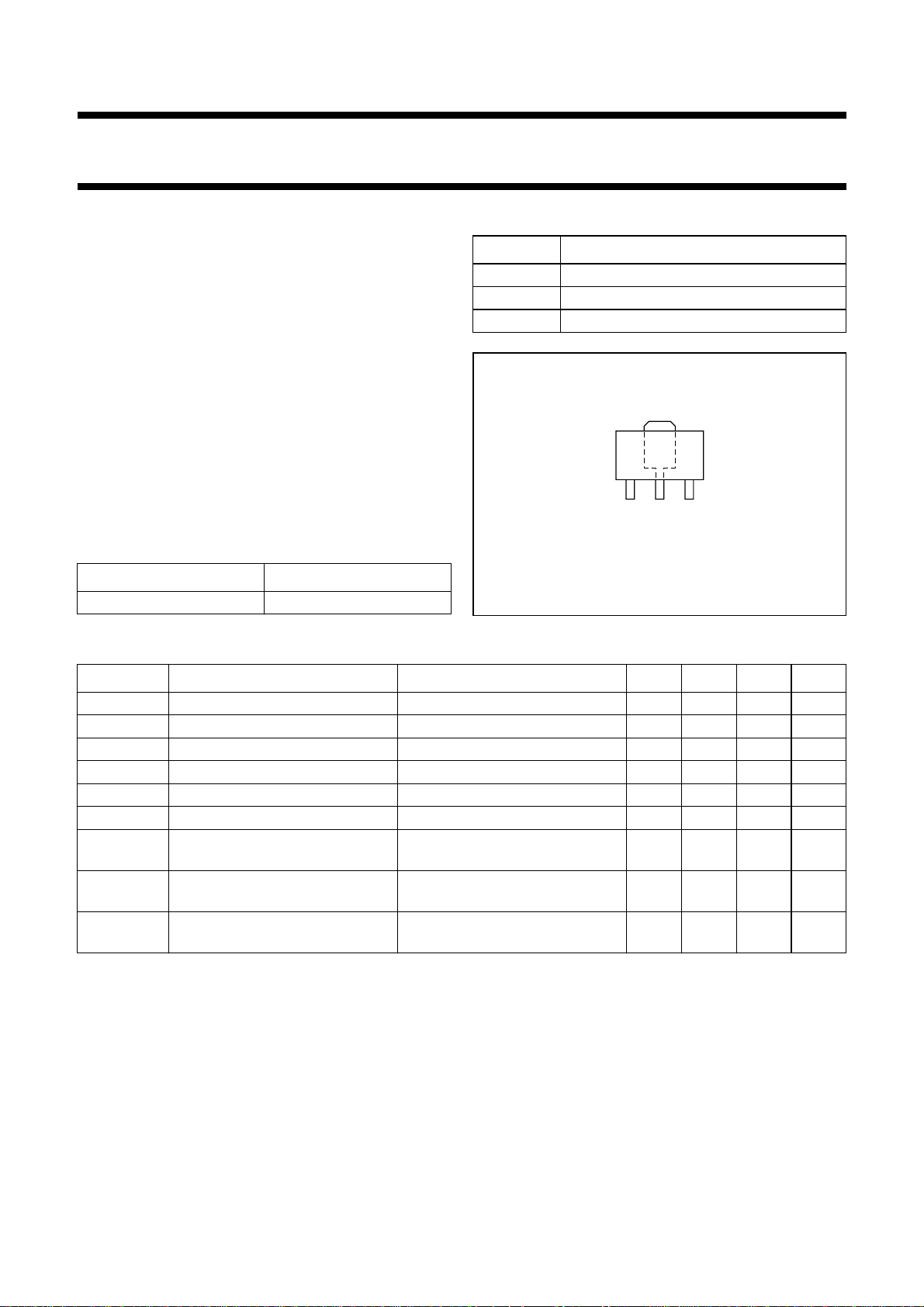
PINNING
PIN DESCRIPTION
1 emitter
2 collector
3 base
321
Fig.1 Simplified outline (SOT89).
SYMBOL PARAMETER CONDITIONS MIN. TYP. MAX. UNIT
V
V
I
P
h
C
f
CBO
CEO
C
tot
FE
re
T
collector-base voltage open emitter −−20 V
collector-emitter voltage open base −−15 V
collector current (DC) −−200 mA
total power dissipation Ts≤ 90 °C; note 1 −−2.25 W
DC current gain IC= 70 mA; VCE=8V 6090250
feedback capacitance IC= 0; VCB= 12 V; f = 1 MHz − 0.8 − pF
transition frequency IC= 70 mA; VCE=12V;
− 7 − GHz
f = 1 GHz
G
UM
2
|s
|
21
maximum unilateral power gain IC= 70 mA; VCE=12V;
f = 900 MHz; T
amb
=25°C
insertion power gain IC= 70 mA; VCE=12V;
f = 900 MHz; T
amb
=25°C
− 11 − dB
− 10 − dB
Note
1. T
is the temperature at the soldering point of the collector pin.
s

NXP Semiconductors Product specification
Rev. 04 - 2 October 2007
3 of 11
NPN 7 GHz wideband transistor BFQ591
LIMITING VALUES
In accordance with the Absolute Maximum System (IEC 60134).
SYMBOL PARAMETER CONDITIONS MIN. MAX. UNIT
V
CBO
V
CEO
V
EBO
I
C
P
tot
T
stg
T
j
Note
1. Tsis the temperature at the soldering point of the collector pin.
THERMAL CHARACTERISTICS
collector-base voltage open emitter − 20 V
collector-emitter voltage open base − 15 V
emitter-base voltage open collector − 3V
collector current (DC) − 200 mA
total power dissipation Ts≤ 90 °C; note 1 − 2.25 W
storage temperature −65 +150 °C
junction temperature − 175 °C
SYMBOL PARAMETER CONDITIONS VALUE UNIT
R
th j-s
thermal resistance from junction
Ts≤ 90 °C; note 1 38 K/W
to soldering point
Note
1. Tsis the temperature at the soldering point of the collector pin.
NXP Semiconductors Product specification
Rev. 04 - 2 October 2007
4 of 11
NPN 7 GHz wideband transistor BFQ591
CHARACTERISTICS
Tj=25°C; unless otherwise specified.
SYMBOL PARAMETER CONDITIONS MIN. TYP. MAX. UNIT
V
(BR)CBO
V
(BR)CES
V
(BR)EBO
I
CBO
h
FE
C
re
f
T
G
UM
|s21|
V
o
2
collector-base breakdown voltage IC= 0.1 mA; IE=0 −−20 V
collector-emitter breakdown
IC= 0.1 mA; IB=0 −−15 V
voltage
emitter-base breakdown voltage IE= 0.1 mA; IC=0 −−3V
collector-base leakage current IE= 0; VCB=10 −−100 nA
DC current gain IC=70mA; VCE=8V 6090250
feedback capacitance IC= 0; VCB= 12 V; f = 1 MHz − 0.8 − pF
transition frequency IC= 70 mA; VCE=12V;
− 7 − GHz
f = 1 GHz
maximum unilateral power gain;
note 1
IC= 70 mA; VCE=12V;
T
=25°C
amb
f = 900 MHz − 11 − dB
f = 2 GHz − 5.5 − dB
insertion power gain IC= 70 mA; VCE=12V;
f = 1 GHz; T
amb
=25°C
− 10 − dB
output voltage note 2 − 700 − mV
Notes
2
s
1. G
is the maximum unilateral power gain, assuming s12is zero and .
UM
G
UM
10 log
-------------------------------------------------------1s
21
2
–()1s
11
–()
2. dim= 60 dB (DIN45004B); Vp=Vo; Vq=Vo −6 dB; fp= 795.25 MHz; fq= 803.25 MHz; fr= 803.25 MHz;
measured at f
= 793.25 MHz.
(p+q+r)
dB=
2
22

NXP Semiconductors Product specification
Rev. 04 - 2 October 2007
5 of 11
NPN 7 GHz wideband transistor BFQ591
P
(W)
3
tot
2
1
0
0
handbook, halfpage
50 100 200
150
Fig.2 Power derating curve.
MLD796
Ts (°C)
250
handbook, halfpage
h
FE
200
150
100
50
0
−2
10
VCE=12V.
−1
10
11010
MRA749
IC (mA)
Fig.3 DC current gain as a function of collector
current; typical values.
2
1.2
handbook, halfpage
C
re
(pF)
0.8
0.4
0
0
IC= 0; f = 1 MHz.
48 16
12
VCB (V)
Fig.4 Feedback capacitance as a function of
collector-base voltage; typical values.
MLD797
handbook, halfpage
8
f
T
(GHz)
6
4
2
0
1
VCE= 12 V; f = 1 GHz.
10 10
IC (mA)
Fig.5 Transition frequency as a function of
collector current.
MLD798
2

NXP Semiconductors Product specification
Rev. 04 - 2 October 2007
6 of 11
NPN 7 GHz wideband transistor BFQ591
25
handbook, halfpage
gain
(dB)
20
15
10
5
0
0
VCE= 12 V; f = 900 MHz.
40 80
IC (mA)
Fig.6 Gain as a function of collector current;
typical values.
MLD799
G
max
G
UM
120
10
handbook, halfpage
gain
(dB)
8
6
4
2
0
0
VCE= 12 V; f = 2 GHz.
40 80
IC (mA)
Fig.7 Gain as a function of collector current;
typical values.
MLD800
MSG
G
UM
120
40
handbook, halfpage
gain
(dB)
30
MSG
20
10
0
10
IC= 70 mA; VCE=12V.
G
UM
2
10
G
max
MSG
3
10
f (MHz)
Fig.8 Gain as a function of frequency; typical
values.
MLD801
4
10

NXP Semiconductors Product specification
Rev. 04 - 2 October 2007
7 of 11
NPN 7 GHz wideband transistor BFQ591
−30
handbook, halfpage
d
im
(dB)
−40
−50
−60
−70
04080
Vo= 700 mV; VCE= 12 V; T
amb
=25°C; f
(p+q+r)
IC (mA)
= 793.25 MHz.
Fig.9 Intermodulation distortion as function of
collector current; typical values.
MLD802
120
−30
handbook, halfpage
d
2
(dB)
−40
−50
−60
−70
−80
04080
Vo= 316 mV; VCE= 12 V; f
(p+q)
= 810 MHz.
MLD803
IC (mA)
Fig.10 Second order intermodulation distortion as
function of collector current; typical values.
120

NXP Semiconductors Product specification
Rev. 04 - 2 October 2007
8 of 11
NPN 7 GHz wideband transistor BFQ591
SPICE parameters for the BFQ591 die.
SEQUENCE No. PARAMETER VALUE UNIT
1 IS 1.341 fA
2 BF 123.5 −
3 NF .988 −
4 VAF 75.85 V
5 IKF 9.656 mA
6 ISE 232.2 fA
7 NE 2.134 −
8 BR 10.22 −
9 NR 1.016 −
10 VAR 1.992 V
11 IKR 294.1 mA
12 ISC 211.0 aA
13 NC 997.2 −
14 RB 5.00 Ω
15 IRB 1.000 µA
16 RBM 5.00 Ω
17 RE 1.275 Ω
18 RC 920.6 Ω
(1)
19
20
21
(1)
(1)
XTB 0.000 −
EG 1.110 eV
XTI 3.000 −
22 CJE 3.821 pF
23 VJE 600.0 mV
24 MJE 348.5 −
25 TF 13.60 ps
26 XTF 71.73 −
27 VTF 10.28 V
28 ITF 1.929 mA
29 PTF 0.000 deg
30 CJC 1.409 fF
31 VJC 219.4 mV
32 MJC 166.5 −
33 XCJ 2.340 −
34 TR 543.7 ps
(1)
35
36
37
(1)
(1)
CJS 0.000 F
VJS 750.0 mV
MJS 0.000 −
38 FC 733.2 −
handbook, halfpage
L1 L2
B
C
QLB= 50;QLE= 50;QL
= scaling frequency = 1 GHz.
f
c
L
be ce
B,E
Fig.11 Package equivalent circuit SOT89.
List of components (see Fig.11)
DESIGNATION VALUE UNIT
C
be
C
cb
C
ce
L1 1 nH
L2 0.01 nH
L3 1 nH
L
B
L
E
C
cb
B
E'
L
L3
E
(f)=QL
B,E
√(f/fc);
16 fF
150 fF
150 fF
1.2 nH
1.2 nH
CB' C'
C
E
MBC964
Note
1. These parameters have not been extracted, the
default values are shown.

NXP Semiconductors Product specification
Rev. 04 - 2 October 2007
9 of 11
NPN 7 GHz wideband transistor BFQ591
PACKAGE OUTLINE
Plastic surface-mounted package; collector pad for good heat transfer; 3 leads SOT89
w M
D
b
p3
123
b
p2
B
b
p1
e
1
e
B
A
E
L
p
H
E
c
DIMENSIONS (mm are the original dimensions)
UNIT
mm
0 2 4 mm
scale
A
1.6
1.4
OUTLINE
VERSION
SOT89 TO-243 SC-62
b
p1
0.48
0.35
b
p2
0.53
0.40
IEC JEDEC JEITA
b
1.8
1.4
p3
c
0.44
0.23
D
E
4.6
2.6
4.4
2.4
REFERENCES
e
3.0
1.5
H
L
1.2
0.8
w
p
0.13
EUROPEAN
PROJECTION
ISSUE DATE
06-03-16
06-08-29
e
E
1
4.25
3.75

NXP Semiconductors
Rev. 04 - 2 October 2007
10 of 11
Legal information
Data sheet status
BFQ591
NPN 7 GHz wideband transistor
Document status
Objective [short] data sheet Development This document contains data from the objective specification for product development.
Preliminary [short] data sheet Qualification This document contains data from the preliminary specification.
Product [short] data sheet Production This document contains the product specification.
[1] Please consult the most recently issued document before initiating or completing a design.
[2] The term ‘short data sheet’ is explained in section “Definitions”.
[3] The product statusof device(s) described in this document may have changed since this document was published and may differ in case of multiple devices. The latest product status
information is available on the Internet at URL
[1][2]
Product status
Definitions
Draft — The document is a draft version only. The content is still under
internal review and subject to formal approval, which may result in
modifications or additions. NXP Semiconductors does not give any
representations or warranties as to the accuracy or completeness of
information included herein and shall haveno liability for the consequences of
use of such information.
Short data sheet — A short data sheet is an extract from a full data sheet
with the same product type number(s) and title. A short data sheet is intended
for quick reference only and should not be relied upon to contain detailed and
full information. For detailed and full information see the relevant full data
sheet, which is available on request via the local NXP Semiconductors sales
office. In case of any inconsistency or conflict with the short data sheet, the
full data sheet shall prevail.
Disclaimers
General — Information in this document is believed to be accurate and
reliable. However,NXP Semiconductors does not give any representations or
warranties, expressed or implied, as to the accuracy or completeness of such
information and shall have no liability for the consequences of use of such
information.
Right to make changes — NXP Semiconductors reserves the right to make
changes to information published in this document, including without
limitation specifications and product descriptions, at any time and without
notice. This document supersedes and replaces all information supplied prior
to the publication hereof.
Suitability for use — NXP Semiconductors products are not designed,
authorized or warranted to be suitable for use in medical, military, aircraft,
space or life support equipment, nor in applications where failure or
[3]
http://www.nxp.com.
Definition
malfunction of a NXP Semiconductors product can reasonably be expected to
result in personal injury, death or severe property or environmental damage.
NXP Semiconductors accepts no liability for inclusion and/or use of NXP
Semiconductors products in such equipment or applications and therefore
such inclusion and/or use is at the customer’s own risk.
Applications — Applications that are described herein for any of these
products are for illustrative purposes only. NXP Semiconductors makes no
representation or warranty that such applications will be suitable for the
specified use without further testing or modification.
Limiting values — Stress above one or more limiting values (as defined in
the Absolute Maximum Ratings System of IEC 60134) may cause permanent
damage to the device. Limiting values are stress ratings only and operation of
the device at these or any other conditions above those given in the
Characteristics sections of this document is not implied. Exposure to limiting
values for extended periods may affect device reliability.
Terms and conditions of sale — NXP Semiconductors products are sold
subject to the general terms and conditions of commercial sale, as published
http://www.nxp.com/profile/terms, including those pertaining to warranty,
at
intellectual property rights infringement and limitation of liability, unless
explicitly otherwise agreed to in writing by NXP Semiconductors. In case of
any inconsistency or conflict between information in this document and such
terms and conditions, the latter will prevail.
No offer to sell or license — Nothing in this document may be interpreted
or construed as an offer to sell products that is open for acceptance or the
grant, conveyance or implication of any license under any copyrights, patents
or other industrial or intellectual property rights.
Trademarks
Notice: All referenced brands, product names, service names and trademarks
are the property of their respective owners.
Contact information
For additional information, please visit: http://www.nxp.com
For sales office addresses, send an email to: salesaddresses@nxp.com

NXP Semiconductors
BFQ591
NPN 7 GHz wideband transistor
Revision history
Revision history
Document ID Release date Data sheet status Change notice Supersedes
BFQ591_N_4 20071002 Product data sheet - BFQ591_3
Modifications:
BFQ591_3 20020204 Product specification - BFQ591_N_2
BFQ591_N_2
(9397 750 09252)
BFQ591_N_1
(9397 750 09013)
• Fig. 1 and package outline updated
20020102 Preliminary specification BFQ591_N_1
20011203 Preliminary specification - -
Please be aware that important notices concerning this document and the product(s)
described herein, have been included in section ‘Legal information’.
© NXP B.V. 2007. All rights reserved.
For more information, please visit: http://www.nxp.com
For sales office addresses, please send an email to: salesaddresses@nxp.com
Date of release: 2 October 2007
Document identifier: BFQ591_N_4
 Loading...