

Page 1

User Guide
NVIDIA nForce 590 SLI
Technology Chipset Overclocking
May 2005
DU-02451-001_v01
Page 2

Document Change History
Version Date Responsible Reason for Change
01 05/17/06 WZ, TS, NSmith Initial release.
DU-02451-001_v01 ii
05/17/06
Page 3

Table of Contents
NVIDIA nForce 590 SLI Technology Chipset Overclocking ...........................................1
Key Concepts.........................................................................................................2
Cooling...............................................................................................................2
Power Supply Units .............................................................................................2
Glossary of Terms ..................................................................................................3
Overclocking the NVIDIA nForce 590 SLI Technology Chipset......................................5
Disable AMD Cool’n’Quiet Technology......................................................................7
A Systematic Approach ...........................................................................................8
CPU Reference Clock...........................................................................................9
CPU HyperTransport Overclocking......................................................................15
CPU Core Clock.................................................................................................17
DDR2 Memory Interface Overclocking ................................................................19
Balance CPU Frequency, HyperTransport, and Memory Overclocking Results ........24
PCI Express Overclocking ..................................................................................25
NVIDIA nForce 590 SLI MCP HyperTransport Interface........................................27
GPU Overclocking..............................................................................................29
Overclocking the System.......................................................................................30
Final Thoughts.........................................................................................................33
DU-02451-001_v01 iii
05/17/06
Page 4

List of Figures
Figure 1. High-level System Diagram.....................................................................6
Figure 2. Power Management Setup SBIOS Menu ..................................................7
Figure 3. System Clock Setup for CPU Reference Clock Overclocking.....................10
Figure 4. Memory Settings for CPU Reference Clock Overclocking.........................11
Figure 5. System Voltages for Reference Clock Overclocking.................................12
Figure 6. Adjusting CPU Reference Clock using NVIDIA nTune 5.0........................13
Figure 7. NVIDIA nTune 5.0 Stability Test ...........................................................14
Figure 8. System Clocks BIOS Configuration for CPU HTT Overclocking.................15
Figure 9. Adjusting HT Bus Frequency Using NVIDIA nTune 5.0 ...........................16
Figure 10. BIOS System Clocks Configuration for CPU Overclocking........................18
Figure 11. Disabling SLI-Ready Memory in BIOS....................................................20
Figure 12. BIOS System Voltages Configuration for Memory Overclocking...............20
Figure 13. BIOS Memory Timings Settings for Memory Overclocking.......................21
Figure 14. BIOS Drive Strength Setting for Memory Overclocking ...........................22
Figure 15. Memory Overclocking using NVIDIA nTune 5.0......................................23
Figure 16. Overclocking PCI Express using NVIDIA nTune 5.0................................26
Figure 17. BIOS System Voltages Configuration for MCP HTT Overclocking .............27
Figure 18. Adjusting MCP HTT Frequency in BIOS..................................................28
Figure 19. Overclocking GPU using NVIDIA nTune 5.0 ...........................................29
Figure 20. NVIDIA nTune 5.0 Dynamic BIOS Access ..............................................31
Figure 21. Storing Profiles in NVIDIA nTune 5.0 ....................................................32
Figure 22. Loading Automated Settings Using NVIDIA nTune 5.0 Custom Rules.......32
DU-02451-001_v01 iv
05/17/06
Page 5

NVIDIA nForce 590 SLI Technology
Chipset Overclocking
The purpose of this document is to guide users through overclocking NVIDIA
nForce 590 SLI technology chipset and use of the numerous tools and features that
will boost system performance, enhancing end-user gaming experience.
Overclocking PCs was once quite difficult and required people to physically change
hardware. In the past, companies that designed motherboards, CPUs, memory, and
graphics processor units were not supportive of overclocking nor were they
supportive of allowing users to tamper with qualified and tested settings.
Things have changed recently, however. Companies are more accommodating of
the urgent requests PC enthusiasts make. In fact, ASIC designers now incorporate a
lot of performance and overclocking headroom in the chips they produce.
Nowadays, with the availability of highly overclockable PC components and the
utilities that allow users to easily attain higher performance, overclocking has moved
into the mainstream.
NVIDIA
overclockable. These products have provided higher performance for PC gaming
enthusiasts searching for the ultimate gaming experience.
NVIDIA specifically designed the NVIDIA nForce
based on the new AMD AM2 Athlon processor, with overclocking enthusiasts in
mind. Even though the chipset itself is highly overclockable, NVIDIA built an
entire support platform around the NVIDIA nForce 590 SLI core logic. This
platform includes:
®
GPUs have enjoyed good reputations as products that are highly
®
590 SLI™ technology chipset,
Software utilities such as the newly redesigned NVIDIA nTune 5.0 and its
highly sophisticated SBIOS
Special high-performance memory with Enhanced Performance Profiles
Technology
Recommended CPU coolers
NVIDIA SLI
DU-02451-001_v01 1
05/17/06
™
technology.
Page 6

NVIDIA nForce 590 SLI Technology Chipset Overclocking
Key Concepts
Overclocking refers to operating PC components beyond what the manufacturer
guarantees. When overclocking is not carried on with care, it may lead to system
instability, crashes and loss of data, and may even destroy components. However,
when overclocking is performed attentively, it increases overall system performance
quite dramatically.
Cooling
Cooling PC components sufficiently is critical to overclocking. Keeping the CPU,
GPU, or overall system cool all contribute to overall system overclockability.
Otherwise, higher component temperatures lead to operation instability and
increased power consumption.
Theoretically, frequency is directly proportional to power and temperature. The
higher the frequency, the more the power consumed and the hotter the device
becomes. In order to achieve higher frequencies, component temperatures should
be kept as low as possible. With proper cooling, overclocking is highly attainable.
The most commonly cooling techniques are air cooling with fan-mounted heat sinks
and water cooling blocks. Even though water cooling is harder to install, it achieves
higher overclockability in comparison to air cooling because it keeps temperatures
lower. With technological advancements, air cooling has improved in performance
providing the means for overclocking. Even so, water cooling CPUs and GPUs is
becoming more widely accepted.
For NVIDIA recommended CPU coolers, visit
components.
Power Supply Units
Power supply units are also important when it comes to overclocking. Increasing
system performance leads to increased power consumption by the overclocked
components. Having a power supply that generates enough power with headroom
is essential in guaranteeing system stability. Check the following site for a list of
power supplies suitable for SLI systems:
www.slizone.com/object/slizone2_build.html#certified_powersupplies.
www.SLIZone.com/nForce for a list of
DU-02451-001_v01 2
05/17/06
Page 7

NVIDIA nForce 590 SLI Technology Chipset Overclocking
Glossary of Terms
3DMark
AMD
Cool’n’Quiet
Technology
BIOS
CPU HTT
CPU HTT
Reference
Clock
Multiplier
Prime95
Synthetic 3D benchmark that provides a measure of graphics
performance. It is also often used to test a system for stability.
Technology that changes CPU frequency dynamically depending
™
on power and thermal requirements of a CPU. Because it limits
the overclockability of an AMD CPU, it needs to be turned off
for best results.
For more information, visit this link
en/Processors/ProductInformation/0,,30_118_9485_9487%5E10272,00.html.
http://www.amd.com/us-
Basic Input Output System.
HyperTransport interface connecting the AMD CPU to NVIDIA
nForce 590 SLI SPP. Nominally, it runs at 1 GHz clock or 4
GBps in downstream and upstream directions.
Clock signal of the CPU HyperTransport link. It has impact on
HyperTransport bus speed, CPU frequency, as well as memory
frequency. It is 200 MHz nominally.
Multiplier for your front-side bus (FSB). Multiply this value by the
speed of your FSB to get the end CPU clock speed:
CPU Clock Speed = Multiplier x FSB
Program that searches for very large prime number. It contains
stability tests and is an indication of how robust a system is.
Serious Sam
Video game which is used by overclockers to test system
robustness.
t
RAS
Row Address Strobe time is the amount of time between a row
being activated by precharge and deactivated. A row cannot be
deactivated until
has completed. The lower t
RAS
is, the faster
RAS
t
the performance. If it is set too low, it can cause data corruption
by deactivating the row too soon.
tWR
Write Recovery time is the memory timing that determines the
delay between a write command and when a precharge command
is set to the same bank of memory.
t
WRRD
W to R Termination Turnaround time is the number of clock
cycles between the last write data pair and the subsequent READ
command to the same physical bank.
t
RCD
RAS to CAS Access time is the amount of time in cycles for
issuing an active command and the read/write commands.
DU-02451-001_v01 3
05/17/06
Page 8

NVIDIA nForce 590 SLI Technology Chipset Overclocking
t
RRD
t
REF
tRP
t
RWT
t
RDRD
tRC
t
WTR
RAS to RAS Delay is the amount of cycles that it takes to activate
the next bank of memory. The lower the timing, the better the
performance but it can cause instability.
Refresh Rate is the amount of time it takes before a change is
refreshed. If the charge is not refreshed enough, the signal loses
its charge and corrupts data. It is measured in microseconds.
Row Precharge time is the minimum time between active
commands and the read/writes of the next bank of the memory
module.
Read to Write Delay is when a write command is received, this is
the amount of cycles for the command to be executed.
Read to Read Timing is the number of clock cycles between the
last read and the subsequent READ command to the same
physical bank.
Row Cycle time is the minimum time in cycles it takes a row to
t
= t
+ t
complete a full cycle. This can be determined by
t
is set too short, it can cause data corruption. If t
If
RC
RC
RC
RAS
is set too
.
RP
long, stability increases at the expense of performance.
Write to Read Delay is the amount of cycles required between a
valid write command and the next read command. Lower is
better performance but can cause instability.
t
tCL
t
WRWR
CPC
Write to Write time is the number of clock cycles between the last
write and the subsequent WRITE command to the same physical
bank.
CAS latency is the number of clock cycles between the memory
receiving a
READ command and actually starting to read
Command per Clock has only two values: 1 and 2. When set to 1,
it provides the best performance but limits memory frequency. In
order to overclock memory frequency, a value of 2 is more
reasonable.
DU-02451-001_v01 4
05/17/06
Page 9

Overclocking the NVIDIA
nForce 590 SLI Technology Chipset
This section describes how to maximize the performance of an NVIDIA nForce
590 SLI PC system. It provides a systematic approach to unleashing its immense
performance potential. Bus speeds, bandwidth and processor core speeds — both
CPU and GPU core speeds — are the main contributing factors to boosting overall
system performance.
This section describes how to adjust settings for the major chip interconnects and
components that affect performance. Figure 1 shows a high-level diagram of
components in a PC system:
AMD Athlon CPU core frequency
DDR2 memory interface bandwidth and latency
CPU-NVIDIA nForce 590 SLI SPP HyperTransport bus
NVIDIA nForce 590 SLI SPP-NVIDIA nForce 590 SLI MCP
HyperTransport bus
NVIDIA nForce 590 SLI SPP/MCP PCI Express bus
GPU core and memory frequency
DU-02451-001_v01 5
05/17/06
Page 10

NVIDIA nForce 590 SLI Technology Chipset Overclocking
Figure 1. High-level System Diagram
DU-02451-001_v01 6
05/17/06
Page 11
NVIDIA nForce 590 SLI Technology Chipset Overclocking
Disable AMD Cool’n’Quiet
Technology
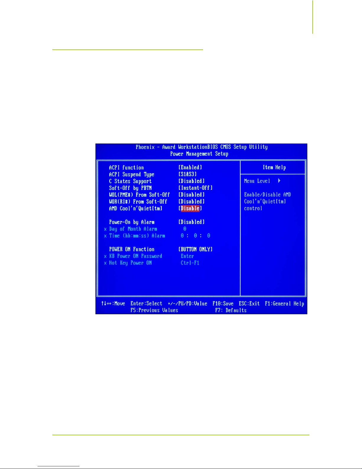
Before overclocking, disable the AMD Cool’n’Quiet™ technology.
The AMD Cool’n’Quiet technology must be disabled in order to enable stable
overclocking without limiting maximum achieved CPU performance. Use the
following procedure to disable this feature:
1. Set AMD Cool’n’Quiet to Disable on the Advanced Power Management
BIOS menu as shown in Figure 2.
Figure 2. Power Management Setup SBIOS Menu
2. Save the configuration.
3. Exit from the BIOS.
DU-02451-001_v01 7
05/17/06
Page 12

NVIDIA nForce 590 SLI Technology Chipset Overclocking
A Systematic Approach
A step-by-step approach helps simplify the complex task of overclocking, described
in the following steps:
1. CPU reference clock (HTT)
2. CPU HyperTransport interface speed
3. CPU core clock frequency
4. DDR2 memory interface frequency & timing
5. Balance the results achieved with CPU frequency, HyperTransport, and
memory overclocking
6. Overclock the PCI Express x16 buses
7. Increase the NVIDIA nForce 590 SLI MCP HyperTransport bus frequency
8. Boost the GPU core and memory frequencies
Each of the following sections provides guidance on how to tweak an NVIDIA
nForce 590-SLI technology chipset based PC system based on this step-by-step
approach.
The first steps for overclocking the CPU reference clock, CPU HyperTransport bus,
CPU frequency, memory interface, PCI Express, and MCP HyperTransport link are
done in the SBIOS. Some system settings, such as CPU multiplier and memory
drive strength parameters, can only be adjusted in the SBIOS.
Once you use the SBIOS for an initial pass at overclocking, you then fine-tune the
settings with NVIDIA nTune 5.0. NVIDIA nTune provides flexibility to adjust
majority of parameters that affect overclocking in a Windows environment, allowing
for dynamic system overclocking and stability testing without the need for constant
system reboots.
Note: Start NVIDIA nTune 5.0 from Programs > NVIDIA Corporation >
nTune. Refer to the application’s on-line help for more information about
the nTune 5.0 features and settings.
The system configuration used in developing this guide is as follows:
CPU: AMD Athlon™ FX-62
Motherboard: Foxconn C51XEM2AA
Graphics: Dual NVIDIA GeForce 7900GTX SLI
CPU Cooler: Zalman CNPS9500AM2
Memory: Corsair TWIN2X2048-8500C5 with Enhanced
Performance Profiles (EPP) Technology
DU-02451-001_v01 8
05/17/06
Page 13

NVIDIA nForce 590 SLI Technology Chipset Overclocking
CPU Reference Clock
CPU reference clock refers to the HyperTransport reference clock signal of the bus
connecting the CPU to NVIDIA nForce 590 SLI SPP chip. Typically, CPU
reference clock frequency is 200 MHz.
Updating the CPU reference clock requires several steps, described in this section:
1. Change system clocks in system BIOS menu.
2. Change memory timings in system BIOS menu.
3. Change system voltages in system BIOS menu.
4. Fine-tune the CPU reference clock in the motherboard settings control panel
of nTune.
5. Text the stability of the system
Because the CPU reference clock value direct impacts CPU core frequency and
HyperTransport bandwidth, take some time to determine the maximum attainable
CPU reference clock. To do so, use the following formulas:
CPU core frequency = CPU reference clock (MHz) × CPU multiplier
HyperTransport bus speed = CPU reference clock (MHz) × HT multiplier
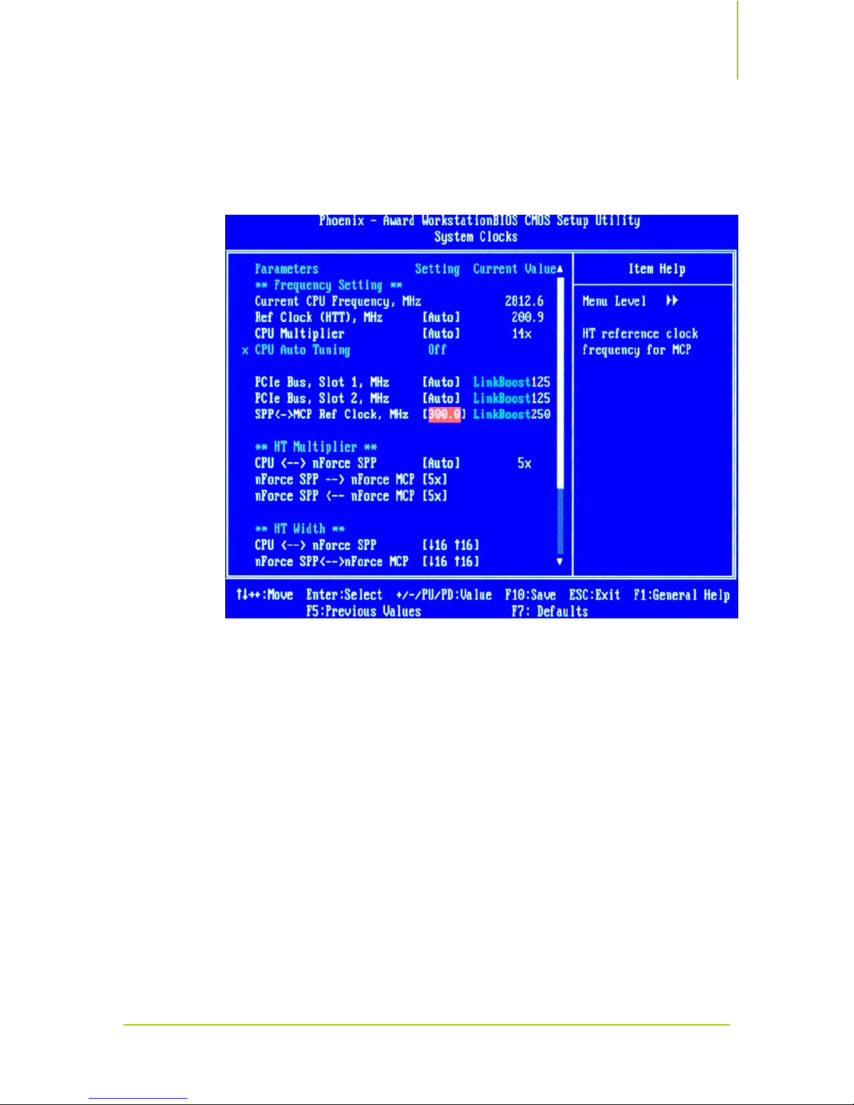
Change System Clocks
Before you can find the maximum CPU reference clock the NVIDIA nForce 590
SLI motherboard is capable of achieving, you must make sure all reasons for
instability in the system are eliminated. Possible causes of instability include
undesirable values for CPU core clock, HyperTransport frequency, and memory
frequency. Make sure these are set well within their specifications in order to isolate
the root cause of issues that may arise from increasing the CPU reference clock
frequency.
When the system shows signs of instability, use the following procedure and the
BIOS menu shown in Figure 3 to reconfigure the system to better isolate the root
cause of issues:
1. Lower the
other AM2 CPUs x5 will work) in
2. Change
3. Set the
the CPU reference clock later using nTune.
CPU Multiplier to x9 (for FX-62 CPU, this value is sufficient; for
CPU <-> nForce SPP multiplier to x3.
Ref Clock (HTT) to 250 MHz as a starting point. You can fine-tune
System Clocks BIOS menu.
DU-02451-001_v01 9
05/17/06
Page 14

NVIDIA nForce 590 SLI Technology Chipset Overclocking
Figure 3 shows the proper configuration in preparation for overclocking the CPU
reference clock.
Figure 3. System Clock Setup for CPU Reference Clock
Overclocking
DU-02451-001_v01 10
05/17/06
Page 15

NVIDIA nForce 590 SLI Technology Chipset Overclocking
Set Memory Timings
Set memory frequency as low as possible from the Memory Timings BIOS menu, as
shown in Figure 4:
1. Set
2. Set
Timing Mode to [User limit].
Memory Clock Limit to [DDR2 400].
Figure 4. Memory Settings for CPU Reference Clock
Overclocking
DU-02451-001_v01 11
05/17/06
Page 16

NVIDIA nForce 590 SLI Technology Chipset Overclocking
Change System Voltages
To enable increases in the CPU reference clock frequency, increase the following
voltages. Go to the
match the values shown in Figure 5:
System Voltages BIOS menu and change the following to
1. Change CPU core voltage,
2. Change HyperTransport interface core voltage,
CPU.
HT CPU <-> nForce SPP.
3. Change NVIDIA nForce 590 SLI SPP and MCP core voltage,
nForce MCP.
and
nForce SPP
Figure 5. System Voltages for Reference Clock Overclocking
4. Save all BIOS settings.
5. Reboot to Windows.
DU-02451-001_v01 12
05/17/06
Page 17

NVIDIA nForce 590 SLI Technology Chipset Overclocking
Fine-Tune CPU Reference Clock
Go to NVIDIA nTune 5.0 to adjust the frequency using the Reference Clock
(HTT)
setting from NVIDIA nTune Motherboard Settings control panel as shown
in Figure 6. This action incrementally adjusts the reference clock and allows for
dynamically testing for system stability.
Figure 6. Adjusting CPU Reference Clock using NVIDIA
nTune 5.0
Tip: In nTune, use Left and Right keyboard buttons to make small increments
or decrements for the CPU Reference clock (HTT) slider value.
Incrementing voltages slightly can provide more overclockability.
A CPU reference clock value of 300 MHz is an achievable target, and in some cases
the interface can be overclocked much more depending on the speed of the AMD
FX-62 CPU and nForce 590 SPP chips. Chip speeds vary due to the manufacturing
process variations of the ASICs–application specific integrated circuits.
DU-02451-001_v01 13
05/17/06
Page 18

NVIDIA nForce 590 SLI Technology Chipset Overclocking
Test System Stability
To test system stability, run the NVIDIA Stability Test for at least two hours as seen
in Figure 7. Additionally, running 3DMark, Prime95, or a GPU intensive game like
Serious Sam II for an extended period of time allows you to get a sense of overall
system stability.
Note: CPU reference clock values between 314 MHz to 320 MHz may not
provide system stability.
Figure 7. NVIDIA nTune 5.0 Stability Test
DU-02451-001_v01 14
05/17/06
Page 19

NVIDIA nForce 590 SLI Technology Chipset Overclocking
CPU HyperTransport Overclocking
CPU HyperTransport (HTT) bandwidth (speed) is an important contributing factor
to overall system performance. Its nominal effective bandwidth is 4 GBps running
at 1 GHz (200 MHz × 5) upstream and downstream. CPU HTT bandwidth is
directly proportional to CPU reference clock as mentioned earlier in CPU Reference
Clock on page 9. It defines how fast data propagates between PC devices and CPU
and system memory to maximize throughput. Furthermore, CPU HTT bus speed
has a tremendous impact on memory performance.
Use the following procedure to overclock CPU HyperTransport bandwidth:
1. Eliminate all sources of instability by configuring
settings as shown in Figure 8.
a) Lower the
CPU Multiplier to x10 (for FX-62 CPU, this value is sufficient
and to be safe a x8 multiplier will work; for other AM2 CPUs x5 will
work) in System Clocks BIOS menu.
b) Change
c) Set the
CPU <-> nForce SPP multiplier to x5.
Ref Clock (HTT) to 200 MHz as a starting point. You can fine-
tune the CPU reference clock later using nTune.
System Clocks BIOS
Figure 8. System Clocks BIOS Configuration for CPU HTT
Note: In the Memory Timings BIOS menu, make sure Memory Clock Limit is set
to [DDR2 400] as shown in Figure 4.
DU-02451-001_v01 15
05/17/06
Overclocking
Page 20

NVIDIA nForce 590 SLI Technology Chipset Overclocking
2. Go to NVIDIA nTune to incrementally adjust and test the CPU HTT bus in
Windows. Increasing the
Reference clock (HTT) to 281 MHz provides a
stable setting that effectively increases the CPU HyperTransport speed by
40% to 1.4 GHz, up from 1 GHz. (Check in using the NVIDIA nTune
Motherboard Settings control panel shown in Figure 9).
The CPU HTT interface of NVIDIA nForce 590 SLI motherboards can
support much higher speeds. Adjusting the voltage can help you reach
increases of 50 to 60%.
You can achieve more overclocking by using better cooling systems or by
incrementing voltages slightly (both through the BIOS settings and nTune).
Remember that ASIC and board process variation affects the overclockability
of a system.
Figure 9. Adjusting HT Bus Frequency Using NVIDIA nTune
5.0
3. Run a Stability Test or another application (for example, 3DMark or Serious
Sam) to test system stability.
DU-02451-001_v01 16
05/17/06
Page 21

NVIDIA nForce 590 SLI Technology Chipset Overclocking
CPU Core Clock
This section discusses how to effectively increase the CPU core clock of the AMD
Athlon FX-62 CPU on NVIDIA nForce 590 SLI chipset. Before you proceed to
overclock the CPU core clock, eliminate all other sources of system instability. Do
so by keeping memory and CPU HyperTransport frequencies low.
Use the following procedure to overclock the FX-62 CPU:
1. Go to the
System Voltages BIOS menu to change the following voltages (so
they have exactly the same values as shown in Figure 5):
CPU core voltage
¾
¾ HyperTransport interface core voltage,
¾ NVIDIA nForce 590 SLI SPP core voltage,
HT CPU <-> nForce SPP
nForce SPP and nForce MCP
2. Set memory frequency as low as possible from the
menu so they have exactly the same values as shown in Figure 4.
a) Set
b) Set
Timing Mode to [User limit].
Memory Clock Limit to [DDR2 400].
3. Change the
a) Change the
System Clocks settings to the values shown in Figure 10.
CPU Multiplier to x12 (for FX-62 CPU, this value is
sufficient; for other AM2 CPUs x5 will work) in
menu.
b) Change
c) Set the Ref Clock
CPU <-> nForce SPP multiplier to x3.
(HTT) to 200 MHz as a starting point.
Memory Timings BIOS
System Clocks BIOS
DU-02451-001_v01 17
05/17/06
Page 22

NVIDIA nForce 590 SLI Technology Chipset Overclocking
Figure 10. BIOS System Clocks Configuration for CPU
Overclocking
4. Save BIOS settings and exit.
5. Use NVIDIA nTune 5.0 to change the CPU reference clock by changing the
Reference Clock (HTT) setting.
The AMD Athlon FX-62 CPU runs at 2.8 GHz nominally. When you
increase the reference clock, for instance, to 246 MHz from 200 MHz, you
have overclocked the CPU to 3.07 GHz (256 MHz × 12). You can reach a
higher CPU frequency with by using a better cooling system, by increasing
CPU voltage, or both.
Note: Due to CPU manufacturing process variations, the overclock potential
for CPUs varies. However, AMD FX-62 CPUs typically can overclock to
3.1 to 3.2 GHz using air cooling solutions with a NVIDIA nForce 590
SLI chipset.
DU-02451-001_v01 18
05/17/06
Page 23

NVIDIA nForce 590 SLI Technology Chipset Overclocking
DDR2 Memory Interface Overclocking
Because so much of the memory controller settings can be tuned and because
memory speeds depend on the CPU HTT reference clock and CPU multiplier,
overclocking memory is complicated.
The two approaches to overclocking memory are to:
Increase memory bandwidth by increasing frequency
Decrease memory latency which may lead to frequency reductions
Since different memory devices exhibit different overclocking limitations, some are
more suited for higher frequency while others are best for achieving low CAS
latency. Because this memory device used with the nForce 590 provides higher
performance with increased memory frequency than with reduced latency, this
document focuses on techniques to increase memory bandwidth using Corsair
TWIN2X2048-8500C5 with Enhanced Performance Profiles (EPP) technology.
Rule of Thumb: To decide which approach to overclocking memory works better
for your memory device, calculate the reduction of CAS latency
when the memory is overclocked and divide that value by the
operating memory frequency. The smaller the value, the higher
the throughput and performance will be.
Your two basic options are a faster clock with longer CAS latency
(like tCL = 5) or a slower clock with shorter latency (like tCL = 4).
For example, 5 ÷ CLK1 might be smaller than 4 ÷ CLK2. The
settings with the smallest result will likely provide better
performance, you would choose CLK and tCL = 5.
The AM2 processor’s memory controller architecture is such that the effective
memory frequency is a function of the CPU’s frequency and an internal memory
clock divider. The CPU frequency is also a function of CPU reference clock, or
CPU HyperTransport reference clock, as well as the CPU multiplier. The
relationships are as follows:
Memory frequency = CPU frequency (MHz) ÷ internal integer clock divider
CPU core frequency = CPU reference clock (MHz) × CPU multiplier
A built-in memory clock divider lookup table is used to calculate the memory
frequency. The divider varies based on the memory timings selected (200 MHz, 533
MHz, 667 MHz, and 800 MHz). It increases as the CPU multiplier increase. For
DDR-800 memory setting with an even-numbered CPU multiplier of 10 or above, it
is easy to calculate the memory frequency without knowing what the internal clock
divider is. Multiply 800 MHz by the increase in CPU reference clock with respect to
200 MHz:
Memory frequency = 800 MHz × CPU reference clock ÷ 200 MHz
Before you proceed to overclock the CPU core clock, eliminate all other sources of
system instability.
DU-02451-001_v01 19
05/17/06
Page 24

NVIDIA nForce 590 SLI Technology Chipset Overclocking
Use the following procedure to systematically overclock the DDR2 memory
interface:
1. Turn off
SLI-Ready Memory feature in the Memory Configuration BIOS
menu as shown in Figure 11.
Figure 11. Disabling SLI-Ready Memory in BIOS
2. Go to the
Memory voltage to 2.125 V. To achieve higher clocks, it is often required to
System Voltages BIOS menu shown in Figure 12 to increase the
increase voltage levels while maintaining low device tempuratures.
Figure 12. BIOS System Voltages Configuration for Memory
Overclocking
DU-02451-001_v01 20
05/17/06
Page 25

NVIDIA nForce 590 SLI Technology Chipset Overclocking
3. Change the System Clocks BIOS menu settings so they have exactly the same
values as shown in Figure 10.
a) Change the
CPU Multiplier to x12 (for FX-62 CPU, this value is
sufficient; for other AM2 CPUs x5 will work) in System Clocks BIOS
menu.
b) Change
4. Go to the
CPU <-> nForce SPP multiplier to x3.
Memory Timings BIOS menu shown in Figure 13 and set the
values to match.
Enhanced Performance Profiles (EPP) Technology provides a baseline for
overclocking. Enabling this technology reveals some key memory
performance settings. Adjustments however, are needed to overclock beyond
what EPP technology can provide.
The
Memory Timings BIOS menu displays EPP settings when SLI memory
is enabled and the system is rebooted.
Figure 13. BIOS Memory Timings Settings for Memory
DU-02451-001_v01 21
05/17/06
Overclocking
Page 26

NVIDIA nForce 590 SLI Technology Chipset Overclocking
5. Go to the Driver Strength Settings BIOS menu shown in Figure 14.
The Corsair TWIN2X2048-8500C5 memories can overclock further when
you lower the chip-select (
CS), address (MA), and clock (MCLK) drive strength
settings. Drive strength defines how sharp the edge of a signal transition is.
Lowering the signal drive strength reduces noise injected to neighboring
signals and helps increase frequency.
Note: If you use different memory types, you may discover other tricks and
optimizations by experimenting. For instance, raising the drive strength
may be more a more effective way to tune memory for low latency but
less effective for increasing frequency.
For example, OCZ Technology memories with EPP, lowering data (MD)
and DQS drive strengths by 0.75x produces higher overclocking results.
Figure 14. BIOS Drive Strength Setting for Memory
6. Save BIOS settings and exit.
7. Using NVIDIA nTune 5.0 in Windows, adjust
directly change memory frequency, shown in Figure 15.
DU-02451-001_v01 22
05/17/06
Overclocking
Reference Clock (HTT) to
Page 27

NVIDIA nForce 590 SLI Technology Chipset Overclocking
For DDR2-800 memory, use an even-numbered CPU multiplier of 10 and above:
Effective Memory Frequency = 400 MHz DDR × Reference Clock (HTT) Increase
For example, if the reference clock HTT is set to 250 MHz, the effective memory
frequency will be 500 MHz DDR or 1 GHz:
400 MHz DDR × (250 MHz ÷ 200 MHz)
NVIDIA nTune will report the effective frequency of memory in megahertz.
Figure 15 shows how nTune can be used to overclock memory. Adjusting memory
timings drive strengths, and possible memory and CPU voltages ever so slightly
might be necessary to achieve higher overclockability. Note that the
Strength
is 2 rather than 0. Also, the Reference clock (HTT) setting is 277 MHz
Clock Drive
rather than 300 MHz.
8. Run the Stability Test or 3DMark for an extended period of time to test
system stability with the overclocked memory. The Corsair TWIN2X20488500C5 memories can run well beyond 1.1 GHz.
Figure 15. Memory Overclocking using NVIDIA nTune 5.0
Note: Using odd-numbered CPU multipliers generate lower memory frequency
values than even-numbered multipliers even when using the same reference
clock (HTT) value.
DU-02451-001_v01 23
05/17/06
Page 28

NVIDIA nForce 590 SLI Technology Chipset Overclocking
Balance CPU Frequency, HyperTransport, and Memory
Overclocking Results
Since CPU frequency, HyperTransport bandwidth, and memory frequency
overclocking all depend on CPU HTT reference clock, it is often difficult to obtain
a specific configuration that would generate a maximum overclocking for all.
Hence, overclocking tradeoffs must be made in order to generate the optimum
achievable performance. Higher CPU frequency generally influences performance
the most in comparison to HyperTransport and memory interfaces. 3D applications
are generally CPU-bound, so increasing CPU frequency tremendously boosts
performance. A frequency combination that maximizes CPU frequency is often the
best tradeoff.
Review what you have achieved by following the steps in the previous sections will
provide some guidance as to how a combination can be obtained. As described in
the section called “CPU HyperTransport Overclocking” on page 15, the CPU
HyperTransport interface is capable of running at about 1.4 GHz (280 MHz × 5).
The CPU frequency achieved is 3.07 GHz (256 MHz × 12). Memory is capable of
running at 1,108 MHz:
400 MHz for even-numbered CPU multiplier × percentage overclocking of reference clock
400 MHz × 277 MHz ÷ 200 MHz = 1,108 MHz
Since all three variables have different CPU HTT reference clock settings to achieve
independent overclocking, a value for the reference clock must be selected to
achieve maximum performance for all.
In this case, using 256 MHz as a reference clock generates:
3.07 GHz CPU frequency.
1,280 MHz HyperTransport frequency
1,024 MHz memory frequency
Under other circumstances, however, increasing CPU HTT reference clock and
reducing CPU multiplier while maintaining the same CPU frequency may produce
better results.
It is all about balance. Make it a priority to maximize CPU frequency (sometimes by
lowering the multiplier and raising the CPU HTT). Next, consider memory timings.
In the example setup discussed earlier, the memory frequency is a bit lower than the
physical modules are capable of running. To alleviate this performance reduction
impact, tune latency to improve memory throughput. A memory timing
configuration that reduces
t
, t
, tRP, t
CL
RCD
, tRD, tRC, t
RAS
WTR
, or t
will boost
RAS
performance but might cause instability. Only trial-and-error will help optimize
memory latency. Finally, focus on HyperTransport speed. HyperTransport
overclocking provides some added performance benefit, but its impact is not as
significant as altering CPU frequency and memory performance settings.
Fortunately, NVIDIA nTune 5.0 provides a complete, easy-to-use solution to
optimize memory performance in a Windows environment.
DU-02451-001_v01 24
05/17/06
Page 29

NVIDIA nForce 590 SLI Technology Chipset Overclocking
PCI Express Overclocking
The NVIDIA nForce 590 SLI technology chipset is highly overclockable by design.
™
One of the main features it supports is NVIDIA LinkBoost
technology.
LinkBoost technology is only supported on this chipset and high-end NVIDIA
GeForce products such as the GeForce 7900GTX. LinkBoost technology increases
the PCI Express and HyperTransport link between NVIDIA nForce 590 MCP and
SPP chips by 25% out of the box. PCI Express, however, is far more overclockable
that 25%.
Use the following procedure to overclock the PCI Express interface:
1. Load system configuration defaults in BIOS using Load Defaults option.
2. Go to the
System Voltages BIOS menu to change the following voltages so
they have exactly the same values as shown in Figure 5:
¾ HT nForce SPP <-> MCP
¾ nForce SPP
¾ nForce MCP
3. Use the NVIDIA nTune 5.0 to dynamically change and test each x16 PCI
Express link within the Windows environment.
This will overclock PCI Express on the NVIDIA nForce 590 SLI chipset.
The NVIDIA nForce 590 SLI chipset can sustain PCI Express overclocking
more than 50% nominal. Figure 16 shows how to overclock each of the x16
PCI Express links.
Overclock PCI Express in increments, then test using Stability Test or
another system stress application to ensure proper system functionality after
each increment. Even though the NVIDIA nForce 590 SLI SPP PCI
Express interface might overclock more than its MCP counter part, there is
no performance impact if the two x16 PCI Express interfaces are not
balanced.
DU-02451-001_v01 25
05/17/06
Page 30

NVIDIA nForce 590 SLI Technology Chipset Overclocking
Figure 16. Overclocking PCI Express using NVIDIA nTune 5.0
DU-02451-001_v01 26
05/17/06
Page 31

NVIDIA nForce 590 SLI Technology Chipset Overclocking
NVIDIA nForce 590 SLI MCP HyperTransport Interface
The link between NVIDIA nForce 590 SLI MCP and SPP is a 16-bit upstream and
downstream HyperTransport interface operating at 1 GHz, similar to CPU
HyperTransport interconnect. The NVIDIA LinkBoost technology increases this
bus bandwidth by 25%. Bandwidth increases help with overall system performance.
MCP HyperTransport (HTT) is designed to overclock by up to 50 to 60%.
Overclocking the MCP HTT interface through the BIOS:
1. Load system configuration defaults in BIOS using
Load Defaults option
2. Configure system voltage settings as shown in Figure 17.
Figure 17. BIOS System Voltages Configuration for MCP HTT
Overclocking
DU-02451-001_v01 27
05/17/06
Page 32
NVIDIA nForce 590 SLI Technology Chipset Overclocking
3. To change the frequency, adjust SPP <-> MCP Ref Clock setting in System
Clocks
BIOS menu as illustrated in Figure 18. Gradually increment MCP
HTT clock to determine the highest passing value. MCP HTT clock can run
at 300 MHz and higher.
Figure 18. Adjusting MCP HTT Frequency in BIOS
4. Run a stability test in Windows to test the overclocking.
DU-02451-001_v01 28
05/17/06
Page 33

NVIDIA nForce 590 SLI Technology Chipset Overclocking
GPU Overclocking
GPU overclocking adds a tremendous boost to system gaming performance.
Overclocking the two settings that have the most to do with 3D performance and
gaming will increase GPU performance:
3D frequency
Memory frequency
2D core frequency
Overclocking the GPU can be done using NVIDIA nTune 5.0 as shown in
Figure 19. Although increasing 2D core frequency does not affect 3D applications
and gaming performance, the setting impact 2D applications such as DVD
playback.
The GeForce 7900GTX GPU can overclock to 675 MHz to 710 MHz core
frequency and from 850 MHz to 900 MHz memory frequency using the stock
cooling solution. This alone significantly boosting graphics performance. With
water cooling, the GPU can be overclocked further. Be sure to run Stability Test or
3DMark to test the new overclocked settings.
Figure 19. Overclocking GPU using NVIDIA nTune 5.0
DU-02451-001_v01 29
05/17/06
Page 34

NVIDIA nForce 590 SLI Technology Chipset Overclocking
Overclocking the System
Now that the individual interfaces and system components have been overclocked
independently, combing the new settings generates the best system performance
enhancing the gaming experience.
Conduct overall system stability and burn-in testing to ensure that the new settings
do not impede system stability robustness. Typically, running 3DMark for 24 hours
tests the new system settings adequately. If a system fails, tweak the overclocked
settings to find a stable system configuration. The order of component overclocking
importance relative to performance is as follows:
1. CPU core frequency
2. Optimizing memory performance
3. GPU core and memory frequencies
4. CPU HyperTransport interface bandwidth
5. PCI Express and MCP HyperTransport bus speeds
Upon achieving a stable system configuration, store the new settings and reload
them when starting a new Windows session. NVIDIA nTune 5.0 provides a
comprehensive solution for customizing and retaining settings and retaining
overclock settings. The new
Dynamic BIOS Access feature, shown in Figure 20,
provides easy access to BIOS within a Windows environment. The new clock
settings as well as memory settings are automatically written to BIOS and kick into
effect upon a system reboot.
DU-02451-001_v01 30
05/17/06
Page 35

NVIDIA nForce 590 SLI Technology Chipset Overclocking
Figure 20. NVIDIA nTune 5.0 Dynamic BIOS Access
To retain a complete system configuration of overclocked settings in Windows,
including GPU overclocking, the NVIDIA nTune 5.0
Figure 21. The
Profiles feature lets end users save overclock settings. Once the
settings are configured properly in nTune, save a profile as an “*.nsu” file on the
hard disk drive.
Use the
Custom Rules feature in nTune 5.0 to configure the overclocked settings to
load upon Windows OS initialization. Figure 22 demonstrates how the new settings
can be configured to load upon Windows start up.
Profiles feature, shown in
DU-02451-001_v01 31
05/17/06
Page 36

NVIDIA nForce 590 SLI Technology Chipset Overclocking
Figure 21. Storing Profiles in NVIDIA nTune 5.0
Figure 22. Loading Automated Settings Using NVIDIA nTune
DU-02451-001_v01 32
05/17/06
5.0 Custom Rules
Page 37

Final Thoughts
Overclocking is becoming mainstream practice due to technological advancements
in device manufacturing and the availability of easy-to-use utilities to tune a PC
system. The NVIDIA nForce 590 SLI chipset has been engineered with enthusiasts
and overclockers in mind. An entire platform solution is designed to provide
gaming enthusiasts and overclockers the necessary means to improve their gaming
experience. With new features such as NVIDIA LinkBoost technology, Enhanced
Memory Profiles technology, and NVIDIA nTune 5.0 utility, overclocking
enthusiasts can propel their experiences to new heights.
DU-02451-001_v01 33
05/17/06
Page 38

Notice
ALL NVIDIA DESIGN SPECIFICATIONS, REFERENCE BOARDS, FILES, DRAWINGS, DIAGNOSTICS, LISTS, AND
OTHER DOCUMENTS (TOGETHER AND SEPARATELY, “MATERIALS”) ARE BEING PROVIDED “AS IS.” NVIDIA
MAKES NO WARRANTIES, EXPRESSED, IMPLIED, STATUTORY, OR OTHERWISE WITH RESPECT TO THE
MATERIALS, AND EXPRESSLY DISCLAIMS ALL IMPLIED WARRANTIES OF NONINFRINGEMENT,
MERCHANTABILITY, AND FITNESS FOR A PARTICULAR PURPOSE.
Information furnished is believed to be accurate and reliable. However, NVIDIA Corporation assumes no
responsibility for the consequences of use of such informa ti on or f or any infringement of patents or other
rights of third parties that may result from its use. No license is granted by implication or otherwise under any
patent or patent rights of NVIDIA Corporation. Specifications mentioned in this publication are subject to
change without notice. This public ation supersedes and replaces all information previously supplied. NVIDIA
Corporation products are not authorized for use as critical components in life support devices or systems
without express written approval of NVIDIA Corp oration.
Trademarks
NVIDIA, the NVIDIA logo, SLI, the SLI logo, and nForce are trademarks or registered trademarks of NVIDIA
Corporation. Other company and product names may be trademarks of the respective companies with which
they are associated.
Copyright
© 2006 NVIDIA Corporation. All rights reserved.
NVIDIA Corporation
2701 San Tomas Expressway
Santa Clara, CA 95050
www.nvidia.com
 Loading...