

Page 1

USER GUIDE
Tegra™ 200 Series Developer Board
Advance Information – Subject to Change
NVIDIA CONFIDENTIAL
January 2010 | DG-04927-001_v01
Page 2

Document Change History
Version Date Description
v01 JAN 22, 2010 Initial Release
2 Advance Information – Subject to Change DG-04927-001_v01
NVIDIA CONFIDENTIAL
Page 3

Tegra 200 Series Developer Board User Guide
Table of Contents
1.0 INTRODUCTION .................................................................................................................................................................... 5
2.0 DEVELOPER BOARD OVERVIEW ........................................................................................................................................ 6
2.1 Feature List ........................................................................................................................................................................ 6
2.2 NVIDIA® Tegra™ 250 ........................................................................................................................................................ 8
2.3 System DRAM .................................................................................................................................................................... 8
2.4 Boot Device ........................................................................................................................................................................ 8
2.5 LCD Interface ..................................................................................................................................................................... 9
2.6 External Display Support .................................................................................................................................................... 9
2.7 Audio .................................................................................................................................................................................. 9
2.8 USB .................................................................................................................................................................................... 9
2.9 Storage ............................................................................................................................................................................. 10
2.10 Camera (optional) ........................................................................................................................................................... 10
2.11 Wireless .......................................................................................................................................................................... 10
2.12 User Interface ................................................................................................................................................................. 11
2.13 Miscellaneous ................................................................................................................................................................. 11
2.14 Power ............................................................................................................................................................................. 11
3.0 SATELLITE BOARD HEADERS ........................................................................................................................................... 12
3.1 Satellite Board Headers .................................................................................................................................................... 13
3.2 I2C Map ............................................................................................................................................................................ 14
4.0 CONNECTION EXAMPLES ................................................................................................................................................. 15
4.1 Power ............................................................................................................................................................................... 15
4.1.1 Major Components ...................................................................................................................................................................... 16
4.1.2 Power Supplies ............................................................................................................................................................................ 17
4.1.3 Power Sequencing ...................................................................................................................................................................... 18
4.1.4 Bypass Capacitor Recommendations ......................................................................................................................................... 19
4.1.5 Unused Interface Power Rails ..................................................................................................................................................... 19
4.1.6 Unused Power Management Signals .......................................................................................................................................... 19
4.2 Clocks ............................................................................................................................................................................... 20
4.2.1 32.768KHz Clock ......................................................................................................................................................................... 20
4.2.2 Oscillator Clock ............................................................................................................................................................................ 20
4.3 DRAM Memory Configurations ......................................................................................................................................... 22
4.3.1 Four, 8-bit DDR2 devices ............................................................................................................................................................ 22
4.3.2 Eight, 8-bit DDR2 devices ........................................................................................................................................................... 22
4.3.3 Unused Pins ................................................................................................................................................................................ 23
4.4 NAND ............................................................................................................................................................................... 24
4.5 USB .................................................................................................................................................................................. 24
4.5.1 Force Recovery ........................................................................................................................................................................... 25
4.5.2 ULPI ............................................................................................................................................................................................. 25
4.5.3 PCIe ............................................................................................................................................................................................. 26
DG-04927-001_v01 Advance Information – Subject to Change 3
NVIDIA CONFIDENTIAL
Page 4

Tegra 200 Series Developer Board User Guide
4.6 Display .............................................................................................................................................................................. 27
4.6.1 LCD Displays ............................................................................................................................................................................... 27
4.6.2 HDMI ........................................................................................................................................................................................... 29
4.6.3 VGA (CRT) Out ........................................................................................................................................................................... 30
4.7 Camera ............................................................................................................................................................................. 31
4.7.1 Unused Pins ................................................................................................................................................................................ 31
4.8 SD/SDIO/MMC ................................................................................................................................................................. 32
4.8.1 SD/MMC Card Connections ........................................................................................................................................................ 32
4.8.2 eMMC Device Connections ......................................................................................................................................................... 33
4.8.3 SDIO Device Connections ........................................................................................................................................................... 34
4.8.4 Unused Pins ................................................................................................................................................................................ 34
4.9 Miscellaneous ................................................................................................................................................................... 35
4.9.1 Thermal Diode (Temperature Sensor) ........................................................................................................................................ 35
4.9.2 Debug Interfaces ......................................................................................................................................................................... 35
4.9.3 EFUSE ......................................................................................................................................................................................... 36
4.9.4 Strapping Pins ............................................................................................................................................................................. 37
5.0 THERMAL ............................................................................................................................................................................ 38
5.1 Major Component Thermal Specifications ........................................................................................................................ 38
5.2 Thermal Considerations for Components ......................................................................................................................... 38
DG-04927-001_v01 Advance Information – Subject to Change 4
NVIDIA CONFIDENTIAL
Page 5
Tegra 200 Series Developer Board User Guide
1.0 INTRODUCTION
The Smartbook Development System is an example of a development platform built around the Tegra™ 200 Series Developer
Board. This example provides a starting point for continued development; it outlines a fairly typical Smartbook configuration
based on the NVIDIA® Tegra™ 250 Computer-on-a-Chip.
This document:
Provides recommendations and integration guidelines for engineers to follow when designing a Smartbook or similar
product that is optimized for high performance and low power consumption.
®
Details a generic Smartbook Development System: development system consists of the NVIDIA
Developer Kit plus a satellite board containing most of the user input devices and some features for test and
development; can be used for evaluation and/or software development.
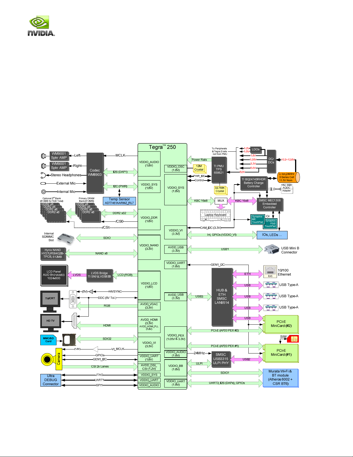
Figure 1. Example Smartbook Development System Block Diagram
Tegra™ 200 Series
DG-04927-001_v01 Advance Information – Subject to Change 5
NVIDIA CONFIDENTIAL
Page 6

2.0 DEVELOPER BOARD OVERVIEW
2.1 Feature List
Tegra 200 Series Developer Board User Guide
Applications Processor
NVIDIA Tegra 250, 23x23mm ,0.8mm pitch
DRAM and Flash Memory
8, 128Mx8, DDR2 @ 333MHz
TPS51116RGET DDR2 Buck Regulator
Hynix 8-bit NAND on board
Internal SD/MMC socket supports eMMC module
Baseband
USB based PCIe Mini Card Modules
USIM Card Connector
Display
LVDS Bridge: TI SN75LVDS83B
HDMI (Type A connector)
Slim 15-pin VGA Connector
Audio
Wolfson WM8903L Codec
Stereo Headphones
External and Internal Mics
Left/Right Speaker Amps.
Imaging
Dual-lane MIPI CSI connection for camera module
Wireless
Murata WiFi and Bluetooth module
- Bluetooth: CSR BC6
- 802.11b/g WiFi: Atheros 6002
-
SD/SDIO and HSMMC
Standard SD/SDIO/MMC socket
USB and Ethernet
SMSC LAN 9514 USB Hub and Ethernet
- 3 USB Type A Host ports
- USB for PCIE MiniCard Slot 2
- Ethernet RJ-45 Jack
SMSC USB3315 ULPI PHY
- USB for PCIE MiniCard Slot 1
USB Mini Type B connector for Recovery Mode
Buttons, Switches
Power-On, Reset and Force-Recovery Buttons
Miscellaneous Devices
EC: SMSC MEC1308
Temperature Sensor: ADT7461AARMZ_RL7
Power
PMIC: TI TPS658621AZGUR
Battery Charge Controller: TI BQ24745RHDR
Main s
Other, lower power regulators
3.3V (standby), 1.2V and 1.5V
Debug / Test Features
22-pin Debug Connector
Tegra Debug Module (optional)
ystem regulators
- 3.3V, 5V, 1.8V and 1.05V
- JTAG, UART and SPI
This is an optional module that may have been shipped with
your Tegra 200 Series Developer Board depending on the
version of the development kit that was ordered.
Power, Reset and Force-Recovery Buttons
Lid Open/Close slider switch
UART4 (4-pin UART) brought to RS232 DB9 serial
connector (intended for software test and debug)
Adds a coin cell battery for uninterrupted Real-Time
Clock operation when the developer board is
powered off
DG-04927-001_v01 Advance Information – Subject to Change 6
NVIDIA CONFIDENTIAL
Page 7

Figure 2. Tegra 200 Series Developer Board (Top View)
LCD (J7)
Camera (J9)
Mini-B
USB
SD/MMC
(J5)
Ethernet
Jack (J4)
VGA Conn
(J12)
Battery
Con
(J14)
AC/DC
Jack
(J15)
Tegra T20
(U4)
HDMI
Conn
(J18)
Tegra 200 Series Developer Board User Guide
WiFi Ant
(J24)
SIM Card
(J19)
PCIE
MiniCard 0
(J27)
PCIE
PMU
(U7)
MiniCard 1
(J27)
Dual USB
Host Ports
(J6)
Headphn
Jack (J1)
Mic Jack
(J2)
Int
Mic
(J8)
Debug
Conn
(J10)
Left
Spkr
(J11)
On
Button
(S1)
Force Rec
Figure 3. Tegra 200 Series Developer Board (Bottom View)
Button
(S2)
DDR2
(Rank 0)
Reset
Button
(S3)
MMC VCORE (J20)
Satellite
Headers
(J16, J17)
Right
Spkr
(J21)
USB Host
Port (J25)
Internal
SD/MMC
(J26)
DG-04927-001_v01 Advance Information – Subject to Change 7
NVIDIA CONFIDENTIAL
Page 8

Tegra 200 Series Developer Board User Guide
2.2 NVIDIA® Tegra™ 250
The NVIDIA Tegra 250 computer-on-a-chip is suited for handheld and mobile applications. It’s primary purpose is to control all
system peripherals and provide computing power.
Table 1 Features (Available / Used on Tegra 200 Series Developer Board)
CPU
External Memory Support
Advanced Power Management
2D/3D acceleration
Connectivity and Expansion
Storage
Multimedia Support
Note:
For more information on Tegra 250, refer to the Tegra 200 Series Datasheet (Electrical, Mechanical and
Thermal Specifications and the Design Guide.
Dual-core ARM® Cortex-A9 MPCore™ processor
32-bit 333MHz DDR2 SDRAM (to 1GB)
2 chip selects
Dynamic voltage and frequency scaling
Multiple clock and power domains
Independent gating of power domains
Integrated Open GLES 2.0 3D core
SPI (Qty 1), I2C (Qty 3), UART (Qty 2)
I2S/PCM (Qty 2)
ULPI HS
USB 2.0 HS (Qty 3)
SDIO (Qty 3)
Internal 4-bit SD/8-bit MMC
o eMMC compatible module available
External 4-bit MMC/SD
Dual Display (Integrated LCD + external)
18-bit LVDS LCD
HDMI to 1080p and VGA
Camera (CSI)
Pre/Post Processing Acceleration with ISP
MPEG-4/H264/JPEG Encoder
2.3 System DRAM
The Tegra 200 Series Developer Board has 8 DDR2 128M x 8 devices for 1GB total system DRAM. The DDR2 will operate up
to 333MHz for a peak bandwidth of 2.7GB/s. The memory is arranged as one or two 32-bit Ranks. Each Rank uses a different
Chip Select and Clock Enable. For low power operation with memory retention, self refresh is supported.
2.4 Boot Device
A 4Gb (512MB) Hynix HY27UF084G2BTPCB 8-bit NAND is available for use as the boot device. In addition, an internal 4-bit
SD, 8-bit MMC socket (J26) is provided to support other flash memories.
DG-04927-001_v01 Advance Information – Subject to Change 8
NVIDIA CONFIDENTIAL
Page 9

Tegra 200 Series Developer Board User Guide
2.5 LCD Interface
The Smartbook Development System routes an 18-bit parallel RGB interface from the Tegra 250 to a Texas Instruments
SN75LVDS83B LVDS Transmitter which goes to an LVDS panel connector (J7). The connector is a Foxconn GS13307-112307F.
The controls available for the panel and backlight include:
Panel power provided by main 3.3V Buck regulator and enabled by the Tegra 250 GPIO on LCD_PWR2
(EN_VDD_PNL)
Backlight enable controlled by the Tegra 250 GPIO on pin SDIO3_DAT2 (SDIO block)
Backlight PWM controlled by PM3_PWM0 on SDIO3_DAT3 (SDIO block)
Backlight power provided from VDD_VBAT (battery or AC/DC adapter) and enabled by the Tegra 250 GPIO on
LCD_CS1_N
LVDS Transmitter shutdown enabled by Tegra 250 GPIO on pin LCD_PWR0
2.6 External Display Support
A standard HDMI Type A connector (J18) is provided and supports up to 1080p60Hz operation. The Tegra 200 Series
Developer Board supports Hot Plug Detect by routing the HP_DET line on the HDMI connector to the Tegra 250 HDMI_INT_N
interrupt pin. The DDC interface is shared between HDMI and the VGA interface, so only one of these displays can be
connected at a time.
A standard 15-pin VGA connector (J12) is also provided and supports resolutions up to 1600x1200. The Tegra 200 Series
Developer Board also supports detection of a VGA device connection. This uses the Tegra 250 pin SPI2_SCK on the Audio
block.
2.7 Audio
The Tegra 200 Series Developer Board integrates the Wolfson Microelectronics WM8903 Ultra Low Power CODEC for Portable
Audio Applications. The Tegra 250 DAP1 interface supporting I2S protocol communicates audio data to/from the CODEC.
GEN1_I2C is used for CODEC configuration. The audio subsystem features:
Left and Right amplified speaker output via two Wolfson WM9001 amplifiers
- Headers for connecting Left (J11)/Right (J21) speakers
Stereo headphone jack (J1)
Both internal Microphone (J8) and external microphone jack (J2)
2.8 USB
The Tegra 250 has three available USB controllers. Controllers #1 and #3 come out on the USB PHYs on the USB1 and USB3
pins. Controller #2 can be used for either ULPI or HSIC (only one at a time). All three USB controllers are used on the Tegra
200 Series Developer Board.
Controller #1
USB1 (PHY) is required for Recovery mode and so is brought out to a USB Mini B connector (J3). USB1 is configured as a
device to allow connection to a host PC, typically for flashing images at the factory or possibly in the field.
Controller #2
USB2 provides a ULPI interface on the Tegra 200 Series Developer Board and connects to an external USB3315 ULPI PHY.
The PHY then connects to PCIe Mini-Card 0 (J27) which is intended for a 3G baseband module.
Controller #3
USB3 (PHY) is routed to an SMSC LAN9514 USB Hub and Ethernet controller. This controller provides one Ethernet interface
and four USB Host ports. The Tegra 200 Series Developer Board routes the Ethernet signals to a standard RJ-45 jack. Three
DG-04927-001_v01 Advance Information – Subject to Change 9
NVIDIA CONFIDENTIAL
Page 10

Tegra 200 Series Developer Board User Guide
of the USB ports are brought to standard Type A connectors (J6 – Dual host port connector and J25 – Single host port). The
forth USB is routed to PCIe Mini-Card #1 (J28).
2.9 Storage
There are two SD/MMC sockets on the Tegra 200 Series Developer Board. Both sockets support High Speed operation
(52MHz for MMC, 50MHz for SD/SDIO)
SD/MMC Socket 1 (J26)
The J26 SD/MMC socket is a combination 8-bit MMC and 4-bit SD/MMC socket intended to be for internal storage, most likely
an eMMC module. Although this device is in a socket, it is not meant to be used as removable storage in a real design. 3.3V is
supplied to the socket. There is also a 2-pin header (J5) to supply a core rail at 2.85V. This header is used when the eMMC
module is installed in this socket.
SD/MMC Socket 2 (J5)
The J5 SD/MMC Socket is a removable storage is a standard 4-bit SD/MMC socket. This would normally be located to allow
SD/MMC/SDIO cards to be inserted and removed by the user. 3.3V is supplied to this socket.
2.10 Camera (optional)
A socket for a camera module is provided on the Tegra 200 Series Developer Board (J9).
2.11 Wireless
Bluetooth and Wifi
The Tegra 200 Series Developer Board integrates a MuRata BT/WF Module using the CSR-BC6 and Atheros AR6002
controllers.
The Bluetooth 2.0 transceiver sends and receives on a 2.4GHz line, including Enhanced Data Rates (EDR) up to 3Mbps and
scatter-net support. USB and Dual UART Ports with rates up to 3MBaud are supported. It operates at full speed Bluetooth
operation with full piconet support and co-exists with 802.11. The CSR device will act as a serial peripheral when connected to
the Tegra 250 via a serial port. This interface, as with WiFi below, will be implemented on a substrate (typically LTCC) supplied
by MuRata containing all components required for operation, to minimize tuning and testing. An external antenna for 2.4GHz
(available off the shelf) is also required
The 802.11b/g transceiver sends and receives on a 2.4GHz line at 54Mbps max. It provides full QoS for 802.11e and security
support 802.11i and co-exists with the Bluetooth device. The interface of choice is SDIO. This interface will be implemented on
a LTCC substrate supplied by MuRata and soldered down to our board to minimize tuning and testing.
An external antenna supporting both Bluetooth and WiFi for 2.4GHz (available off the shelf) is required and available from a
variety of suppliers.
PCIe Mini-Card (3G Modem support and more)
The Tegra 200 Series Developer Board provides two PCIe Mini-Card slots. Both slots support PCIe operation as well as USB
2.0 High Speed. Slot #0 (J27) also routes to a UIM SIM socket (J19) and is intended to support compatible 3G Modem
modules. PCIe Mini-Card slot #1 (J28) could be used for other peripherals such as Solid-State drives or a different WiFi
solution.
Note:
Contact NVIDIA for list of certified PCI express peripherals
DG-04927-001_v01 Advance Information – Subject to Change 10
NVIDIA CONFIDENTIAL
Page 11

Tegra 200 Series Developer Board User Guide
2.12 User Interface
Attach your USB keyboard and mouse to any of the available USB Type-A Host ports (J6, J25).
2.13 Miscellaneous
Temperature Sensor
On Semiconductor Model ADT7461AARMZ_RL7
0.25°C resolution/1°C accuracy (remote channel used)
Interfaces to PWR_I2C
Programmable over/under temperature limits
Debug Options
The Tegra 200 Series Developer Board provides development/debugging interfaces including JTAG, UART and Ethernet.
The Tegra Debug Module [E1173] interfaces to the Tegra 200 Series Developer Board using the expansion headers. This
board provides:
A UART interface through a RS232 DB9 serial connector (intended for software test and debug)
Remote POWER, RESET and FORCE RECOVERY buttons
Adds a coin cell battery for uninterrupted Real-Time Clock operation when the developer board is powered off
2.14 Power
Power Source
Battery: 3-Cell, Li Ion, 24WHr, 11.1V Nominal
AC/DC Adapter: TopMagnetics HK-HW30-A15, 15/30W
- 100V – 240V operation
Battery Charge Controller
Texas Instruments BQ24745RHDR
PMU
Texas Instruments TPS658621AZGUR
Dedicated DC/DCs
Main system 3.3V and 5V rails: Texas Instruments TPS51220ARTVT
Main system 1.8V: Texas Instruments TPS51116RGER
PCIe 1.05V for the Tegra 250: Texas Instruments TPS62290DRVR
External LDOs
1.2V: Texas Instruments TPS72012YZUT
1.5V: Texas Instruments TPS74201RGWR
DG-04927-001_v01 Advance Information – Subject to Change 11
NVIDIA CONFIDENTIAL
Page 12

Tegra 200 Series Developer Board User Guide
3.0 SATELLITE BOARD HEADERS
Two dual row 50-pin expansion headers enable the ability to connect a satellite board to the Tegra 200 Series Developer Board
and are used to extend developer board functionality.
Figure 4. Example Satellite Board Block Diagram
Tegra 200 Series Developer
Board (E1162)
Wireless
Modules
PMU
ONKEY
RESET
I2C
ID
EEPROM
Tegra 2
PWR_I2C
UART4
GPIO
GPIO
GMI_RE_N
PWR_I2C
Tx, Rx, RTS, CTS
Additional Functionality
LEDs (WPAN, WWAN, WLAN)
LEDs (PWR, CHG, NUM,
CAPS, SCROLL, RF)
ONKEY
Button
RF On/Off
Switch
Coin
Cell
RS-232
TRCV
ForceRecovery
RESET
Button
PROG
HDR
DB9
CON
LID_Status
Switch
Button
CAM_I2C
16x8
18x8
Res
Mux
HeartBeat
LED
16x8
I2C
Touchpad
C
or
PS/2
EC
KBC
KBC
GPIO
GPIO
Touchpad
PS/2
DG-04927-001_v01 Advance Information – Subject to Change 12
NVIDIA CONFIDENTIAL
Page 13

Tegra 200 Series Developer Board User Guide
3.1 Satellite Board Headers
All the interface connections between a satellite board and the Tegra 200 Series Developer Board are through two sets of
Samtec FTS series 50-pin Micro Strips connectors.
Table 2. Satellite Connectors Pinout
Dir
Pin # Signal Name
In 1 KB_COL7 EC_KSO17 2 Out Out 1 LED_WPAN* VDD_CELL_RMT 2 In
In 3 KB_COL6 EC_KSO16 4 Out Out 3 LED_WLAN* UART4_TXD 4 Out
In 5 KB_COL5 EC_KSO15 6 Out Out 5 LED_WWAN* VDDIO_NAND_MB 6 Out
In 7 KB_COL4 EC_KSO14 8 Out In 7 W_DISABLE * UART4_RXD 8 In
In 9 KB_COL3 EC_KSO13 10 Out Out 9 LED_WIFI_BT * UART4_CTS* 10 In
In 11 KB_COL2 EC_KSO12 12 Out Out 11 LED_CHARGE* UART4_RTS* 12 Out
In 13 KB_COL1 EC_KSO11 14 Out Out 13 LED_POWER* NO CONNECT 14
In 15 KB_COL0 EC_KSO10 16 Out Out 15 LED_SCROLL_LOCK* FORCE_ACOK 16 In
Out 17 KB_ROW15 EC_KSO9 18 Out Out 17 LED_CAPS_LOCK* VDDIO_SYS_MB 18 Out
Out 19 KB_ROW14 EC_KSO8 20 Out Out 19 LED_NUM_LOCK* PWR_I2C_SCL 20 Bi
Out 21 KB_ROW13 EC_KSO7 22 Out 21 GND PWR_I2C_SDA 22 Bi
Out 23 KB_ROW12 EC_KSO6 24 Out In 23 SPDIF_IN VDD_3V3_MB 24 Out
Out 25 KB_ROW11 EC_KSO5 26 Out Out 25 SPDIF_OUT VDD_3V3_MB 26 Out
Out 27 KB_ROW10 EC_KSO4 28 Out 27 GND GND 28
Out 29 KB_ROW9 EC_KSO3 30 Out Out 29 IR_TXD PS2_TS_CLOCK 30 Bi
Out 31 KB_ROW8 EC_KSO2 32 Out In 31 IR_RXD PS2_TS_DATA 32 Bi
Out 33 KB_ROW7 EC_KSO1 34 Out In 33 LID_OPEN* GND 34
Out 35 KB_ROW6 EC_KSO0 36 Out Out 35 VDD_5V0_MB CAM_I2C_SDA 36 Bi
Out 37 KB_ROW5 EC_KSI7 38 In Out 37 VDD_5V0_MB CAM_I2C_SCL 38 Bi
Out 39 KB_ROW4 EC_KSI6 40 In In 39 TP_IRQ* GND 40
Out 41 KB_ROW3 EC_KSI5 42 In In 41 TS_IRQ* PS2_TP_CLOCK 42 Bi
Out 43 KB_ROW2 EC_KSI4 44 In 43 NO CONNECT PS2_TP_DATA 44 Bi
Out 45 KB_ROW1 EC_KSI3 46 In In 45 ONKEY* LED_HEARTBEAT* 46 Out
Out 47 KB_ROW0 EC_KSI2 48 In In 47 FORCE_RECOVERY* SYS_RESET_B* 48 Out
In 49 EC_KSI0 EC_KSI1 50 In In 49 RESET* VDD_3V3_EC_MB 50 Out
Signal Name Pin #
Dir Dir Pin # Signal Name Signal Name Pin # Dir
DG-04927-001_v01 Advance Information – Subject to Change 13
NVIDIA CONFIDENTIAL
Page 14

Tegra 200 Series Developer Board User Guide
3.2 I2C Map
The I2C interface can be used to connect a touch screen, touch pad and other devices.
There are two options for the Touch devices. I2C versions of these devices (recommended) interface to the Tegra 250, while
PS/2 versions connect to the EC controller.
Table 3. Tegra 200 Series Developer Board I2C Map
Domain Contrlr Pins Volt. Device ID / I2C Addr Location
VDDIO_VI I2C3 CAM_I2C_SCL/SDA 3.3V MEC1308 (I2C Master)
VDDIO_VI I2C3 CAM_I2C_SCL/SDA 3.3V Touchpad 0x28 Remote Location
VDDIO_VI I2C3 CAM_I2C_SCL/SDA 3.3V Touchscreen TBD Remote Location
VDDIO_UART I2C1 GEN1_I2C_SCL/SDA 1.8V Camera 0x36 Main Board
VDDIO_UART I2C1 GEN1_I2C_SCL/SDA 1.8V Autofocus DAC 0x0C Main Board
VDDIO_UART I2C1 GEN1_I2C_SCL/SDA 3.3V Option for SMB to Battery Pack
VDDIO_UART I2C1 GEN1_I2C_SCL/SDA 3.3V Option for SMB to Charger 0x09 Main Board
VDDIO_LCD I2C2 DDC_SCL/SDA 5.0V Mini VGA or HDMI Display 0x30, 0x50, 0x52 Main Board
VDDIO_SYS PWR_I2C PWR_I2C_SCL/SDA 1.8V TI TPS658621 PMU 0x34 Main Board
VDDIO_UART I2C1 1.8V WM8903 Audio Codec 0x1A Main Board
VDDIO_SYS PWR_I2C 1.8V ID EEPROM 0x50 Main Board
VDDIO_SYS PWR_I2C 1.8V ID EEPROM 0x51 Remote Location
VDDIO_SYS PWR_I2C 1.8V Temperature Sensor 0x4C Main Board
Tegra 250 Slave addr:
0x45
Pack is Master or Slave
Slave addr: 0x0B
Main Board
Main Board
Figure 5. I2C Diagram
DG-04927-001_v01 Advance Information – Subject to Change 14
NVIDIA CONFIDENTIAL
Page 15

4.0 CONNECTION EXAMPLES
4.1 Power
Figure 6. Tegra 250 Power Connection Example
Tegra 200 Series Developer Board User Guide
DG-04927-001_v01 Advance Information – Subject to Change 15
NVIDIA CONFIDENTIAL
Page 16

Tegra 200 Series Developer Board User Guide
4.1.1 Major Components
4.1.1.1 PMU
The Tegra 200 Series Developer Board includes a multi-channel power management unit for embedded processors (TI
TPS658621).
Feature List
Host Interface
- I2C Control I/F
- Core/CPU power request signals
- 32.768KHz Clock
- Reset input
- Reset output
RTC LDO
- 1.0V-1.2V nominal voltage range with 25mV steps
- Separate LDO for RTC domain allowing Deep Sleep mode support – the Tegra 250 lowest power mode
- Switch RTC domain automatically back to 1.2V when wake-up event detected (w/CORE_PWR_REQ)
CORE switcher
- 1.0V-1.2V nominal voltage range with 25mV steps
- CORE and RTC domains must track each other within 170mV
- Tracking can be ensured in software
- Optimized DVS handled by NVIDIA BSP (DVFS architecture)
- Turned off if CORE_PWR_REQ is de-asserted – on at 1.2V when CORE_PWR_REQ asserted
CPU switcher
- 0.85-1.0V nominal voltage range with 25mV steps
- Optimized DVS handled by NVIDIA BSP (DVFS architecture)
- Turned off if CPU_PWR_REQ is de-asserted – on at 1.0V when CPU_PWR_REQ asserted
PLL LDO
- Use 1.1V LDO
- Very good line regulation ensured using DC/DC switcher as LDO source
STDBY input
- Standby mode: Only the minimum rails are kept powered (RTC and SYSTEM domains, DDR2 in self-refresh)
- The Tegra 250 indicates Standby mode by de-asserting CORE_PWR_REQ (polarity programmable)
4.1.1.2 Battery Charge Controller
The Tegra 200 Series Developer Board includes a battery charger with input current detect comparator and charge enable pin
(TI bq24745). For a detailed description and list of device features, see http://focus.ti.com/lit/ds/symlink/bq24745.pdf.
4.1.1.3 Battery Pack (Not Included)
The Tegra 200 Series Developer Board can be used with a 3 cell (3S1P) Lithium ion battery pack that has a nominal voltage of
10.8 volts and a total capacity of 2200mAh. The 3S1P is ideal for applications that can operate on lower voltages.
4.1.1.4 External Switchers, LDOs, Power Switches
The Tegra 200 Series Developer Board includes the following components:
Notebook System Power Controller (TI TPS51220): a dual synchronous buck regulator controller with 2 LDOs. For a
detailed description and list of device features, see http://focus.ti.com/lit/ds/sy
DDR2 Memory Power Supply (TI TPS51116): provides a power supply for the DDR2memory system. For a detailed
description and list of device features, see http://focus.ti.com/lit/ds/symlink/tps51116.pdf.
350mA Low-Dropout Linear Regulator (TI TPS72012): for a detailed description and list of device features, see
http://focus.ti.com/lit/ds/sy
Step Down Converter (TI TPS62290): synchronous step down dc-dc converter optimized for battery powered portable
devices. For a detailed description and list of device features, see http://focus.ti.com/lit/ds/sy
135-m Dual Power-Distribution Switch (TI TPS2052): for a detailed description and list of device features, see
http://focus.ti.com/lit/ds/sy
135-m Power Distribution Switch (TI TPS2051): for a detailed description and list of device features, see
http://focus.ti.com/lit/ds/sy
mlink/tps72012.pdf.
mlink/tps2052.pdf.
mlink/tps2051.pdf.
mlink/tps51220.pdf.
mlink/tps62290.pdf.
DG-04927-001_v01 Advance Information – Subject to Change 16
NVIDIA CONFIDENTIAL
 Loading...