

Page 1

NuMicro® NUC029LEE/NUC029SEE
NUMICRO
®
NUC029LEE/NUC029SEE TECHNICAL REFERENCE MANUAL
32-bit Arm® Cortex®-M0 Microcontroller
NuMicro® NUC029 Series
NUC029LEE/NUC029SEE
Technical Reference Manual
The information described in this document is the exclusive intellectual property of
Nuvoton Technology Corporation and shall not be reproduced without permission from Nuvoton.
Nuvoton is providing this document only for reference purposes of NuMicro® microcontroller based system
design. Nuvoton assumes no responsibility for errors or omissions.
All data and specifications are subject to change without notice.
For additional information or questions, please contact: Nuvoton Technology Corporation.
www.nuvoton.com
Aug, 2018 Page 1 of 497 Rev 1.00
Page 2

NuMicro® NUC029LEE/NUC029SEE
NUMICRO
®
NUC029LEE/NUC029SEE TECHNICAL REFERENCE MANUAL
32-bit Arm® Cortex®-M0 Microcontroller
TABLE OF CONTENTS
LIST OF FIGURES ..................................................................................................... 7
LIST OF TABLES ..................................................................................................... 11
1 GENERAL DESCRIPTION ................................................................................... 12
2 FEATURES .......................................................................................................... 13
3 ABBREVIATIONS ................................................................................................ 16
4 PARTS INFORMATION LIST AND PIN CONFIGURATION ................................ 18
4.1 NuMicro® NUC029 Series Selection Code ................................................... 18
4.2 NuMicro® NUC029 Series Selection Guide .................................................. 19
4.3 Pin Configuration ................................................................................. 20
4.3.1 NuMicro® NUC029LEE/NUC029SEE Pin Diagram .............................................. 20
4.4 Pin Description .................................................................................... 22
4.4.1 NuMicro® NUC029LEE/NUC029SEE Pin Description ........................................... 22
5 BLOCK DIAGRAM ............................................................................................... 27
5.1 NuMicro® NUC029LEE/NUC029SEE Block Diagram ...................................... 27
6 FUNCTIONAL DESCRIPTION ............................................................................. 28
6.1 ARM® Cortex®-M0 Core ......................................................................... 28
6.2 System Manager ................................................................................. 30
6.2.1 Overview ................................................................................................ 30
6.2.2 System Reset .......................................................................................... 30
6.2.3 System Power Distribution ........................................................................... 31
6.2.4 System Memory Map ................................................................................. 32
6.2.5 Register Lock ........................................................................................... 33
6.2.6 Auto Trim ................................................................................................ 34
6.2.7 Register Map ........................................................................................... 36
6.2.8 Register Description ................................................................................... 37
6.2.9 System Timer (SysTick) .............................................................................. 74
6.2.10 Nested Vectored Interrupt Controller (NVIC) ...................................................... 79
6.2.11 System Control ....................................................................................... 105
6.3 Clock Controller ................................................................................. 113
6.3.1 Overview .............................................................................................. 113
6.3.2 System Clock and SysTick Clock ................................................................. 116
6.3.3 Power-down Mode Clock ........................................................................... 117
6.3.4 Frequency Divider Output .......................................................................... 117
Aug, 2018 Page 2 of 497 Rev 1.00
Page 3

NuMicro® NUC029LEE/NUC029SEE
NUMICRO
®
NUC029LEE/NUC029SEE TECHNICAL REFERENCE MANUAL
32-bit Arm® Cortex®-M0 Microcontroller
6.3.5 Register Map ......................................................................................... 119
6.3.6 Register Description ................................................................................. 120
6.4 Flash Memory Controller (FMC) ............................................................. 142
6.4.1 Overview .............................................................................................. 142
6.4.2 Features ............................................................................................... 142
6.4.3 Block Diagram ........................................................................................ 143
6.4.4 Functional Description .............................................................................. 144
6.4.5 Register Map ......................................................................................... 154
6.4.6 Register Description ................................................................................. 155
6.5 External Bus Interface (EBI) .................................................................. 164
6.5.1 Overview .............................................................................................. 164
6.5.2 Features ............................................................................................... 164
6.5.3 Block Diagram ........................................................................................ 165
6.5.4 Functional Description .............................................................................. 165
6.5.5 Register Map ......................................................................................... 171
6.5.6 Register Description ................................................................................. 172
6.6 General Purpose I/O (GPIO) ................................................................. 176
6.6.1 Overview .............................................................................................. 176
6.6.2 Features ............................................................................................... 176
6.6.3 Basic Configuration .................................................................................. 177
6.6.4 Functional Description .............................................................................. 177
6.6.5 Register Map ......................................................................................... 180
6.6.6 Register Description ................................................................................. 183
6.7 PDMA Controller (PDMA) ..................................................................... 195
6.7.1 Overview .............................................................................................. 195
6.7.2 Features ............................................................................................... 195
6.7.3 Block Diagram ........................................................................................ 196
6.7.4 Basic Configuration .................................................................................. 197
6.7.5 Functional Description .............................................................................. 197
6.7.6 Register Map ......................................................................................... 200
6.7.7 Register Description ................................................................................. 202
6.8 Timer Controller (TIMER) ..................................................................... 233
6.8.1 Overview .............................................................................................. 233
6.8.2 Features ............................................................................................... 233
6.8.3 Block Diagram ........................................................................................ 234
Aug, 2018 Page 3 of 497 Rev 1.00
Page 4

NuMicro® NUC029LEE/NUC029SEE
NUMICRO
®
NUC029LEE/NUC029SEE TECHNICAL REFERENCE MANUAL
32-bit Arm® Cortex®-M0 Microcontroller
6.8.4 Basic Configuration .................................................................................. 236
6.8.5 Functional Description .............................................................................. 236
6.8.6 Register Map ......................................................................................... 239
6.8.7 Register Description ................................................................................. 241
6.9 PWM Generator and Capture Timer (PWM) ............................................... 250
6.9.1 Overview .............................................................................................. 250
6.9.2 Features ............................................................................................... 251
6.9.3 Block Diagram ........................................................................................ 252
6.9.4 Basic Configuration .................................................................................. 255
6.9.5 Functional Description .............................................................................. 255
6.9.6 Register Map ......................................................................................... 265
6.9.7 Register Description ................................................................................. 267
6.10 Watchdog Timer (WDT) ....................................................................... 295
6.10.1 Overview .............................................................................................. 295
6.10.2 Features ............................................................................................... 295
6.10.3 Block Diagram ........................................................................................ 296
6.10.4 Basic Configuration .................................................................................. 297
6.10.5 Functional Description .............................................................................. 297
6.10.6 Register Map ......................................................................................... 299
6.10.7 Register Description ................................................................................. 300
6.11 Window Watchdog Timer (WWDT) .......................................................... 303
6.11.1 Overview .............................................................................................. 303
6.11.2 Features ............................................................................................... 303
6.11.3 Block Diagram ........................................................................................ 303
6.11.4 Basic Configuration .................................................................................. 304
6.11.5 Functional Description .............................................................................. 304
6.11.6 Register Map ......................................................................................... 307
6.11.7 Register Description ................................................................................. 308
6.12 Real Time Clock (RTC) ........................................................................ 313
6.12.1 Overview .............................................................................................. 313
6.12.2 Features ............................................................................................... 313
6.12.3 Block Diagram ........................................................................................ 314
6.12.4 Basic Configuration .................................................................................. 314
6.12.5 Functional Description .............................................................................. 314
6.12.6 Register Map ......................................................................................... 318
Aug, 2018 Page 4 of 497 Rev 1.00
Page 5

NuMicro® NUC029LEE/NUC029SEE
NUMICRO
®
NUC029LEE/NUC029SEE TECHNICAL REFERENCE MANUAL
32-bit Arm® Cortex®-M0 Microcontroller
6.12.7 Register Description ................................................................................. 320
6.13 UART Interface Controller (UART) .......................................................... 336
6.13.1 Overview .............................................................................................. 336
6.13.2 Features ............................................................................................... 336
6.13.3 Block Diagram ........................................................................................ 337
6.13.4 Basic Configuration .................................................................................. 338
6.13.5 Functional Description .............................................................................. 339
6.13.6 Register Map ......................................................................................... 360
6.13.7 Register Description ................................................................................. 362
6.14 I2C Serial Interface Controller (I2C) .......................................................... 389
6.14.1 Overview .............................................................................................. 389
6.14.2 Features ............................................................................................... 389
6.14.3 Basic Configuration .................................................................................. 390
6.14.4 Block Diagram ........................................................................................ 390
6.14.5 Functional Description .............................................................................. 390
6.14.6 Example for Random Read on EEPROM ....................................................... 403
6.14.7 Register Map ......................................................................................... 405
6.14.8 Register Description ................................................................................. 406
6.15 Serial Peripheral Interface (SPI) ............................................................. 416
6.15.1 Overview .............................................................................................. 416
6.15.2 Features ............................................................................................... 416
6.15.3 Block Diagram ........................................................................................ 417
6.15.4 Basic Configuration .................................................................................. 417
6.15.5 Functional Description .............................................................................. 417
6.15.6 Timing Diagram ...................................................................................... 425
6.15.7 Programming Examples ............................................................................ 428
6.15.8 Register Map ......................................................................................... 430
6.15.9 Register Description ................................................................................. 431
6.16 USB Device Controller (USBD) .............................................................. 447
6.16.1 Overview .............................................................................................. 447
6.16.2 Features ............................................................................................... 447
6.16.3 Block Diagram ........................................................................................ 448
6.16.4 Basic Configuration .................................................................................. 448
6.16.5 Functional Description .............................................................................. 448
6.16.6 Register Map ......................................................................................... 453
Aug, 2018 Page 5 of 497 Rev 1.00
Page 6

NuMicro® NUC029LEE/NUC029SEE
NUMICRO
®
NUC029LEE/NUC029SEE TECHNICAL REFERENCE MANUAL
32-bit Arm® Cortex®-M0 Microcontroller
6.16.7 Register Description ................................................................................. 455
6.17 Analog-to-Digital Converter (ADC) .......................................................... 472
6.17.1 Overview .............................................................................................. 472
6.17.2 Features ............................................................................................... 472
6.17.3 Block Diagram ........................................................................................ 473
6.17.4 Basic Configuration .................................................................................. 473
6.17.5 Functional Description .............................................................................. 474
6.17.6 Register Map ......................................................................................... 481
6.17.7 Register Description ................................................................................. 482
7 ELECTRICAL CHARACTERISTICS ................................ ................................ .. 494
8 PACKAGE DIMENSIONS .................................................................................. 495
8.1 64-pin LQFP (7x7x1.4 mm footprint 2.0 mm) .............................................. 495
8.2 48-pin LQFP (7x7x1.4 mm footprint 2.0 mm) .............................................. 496
9 REVISION HISTORY .......................................................................................... 497
Aug, 2018 Page 6 of 497 Rev 1.00
Page 7

NuMicro® NUC029LEE/NUC029SEE
NUMICRO
®
NUC029LEE/NUC029SEE TECHNICAL REFERENCE MANUAL
32-bit Arm® Cortex®-M0 Microcontroller
LIST OF FIGURES
Figure 4.1-1 NuMicro® NUC029 Series Selection Code ................................................................ 18
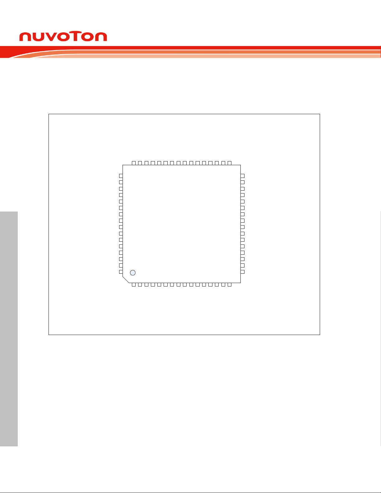
Figure 4.3-1 NuMicro® NUC029SEE LQFP 64-pin Diagram ......................................................... 20
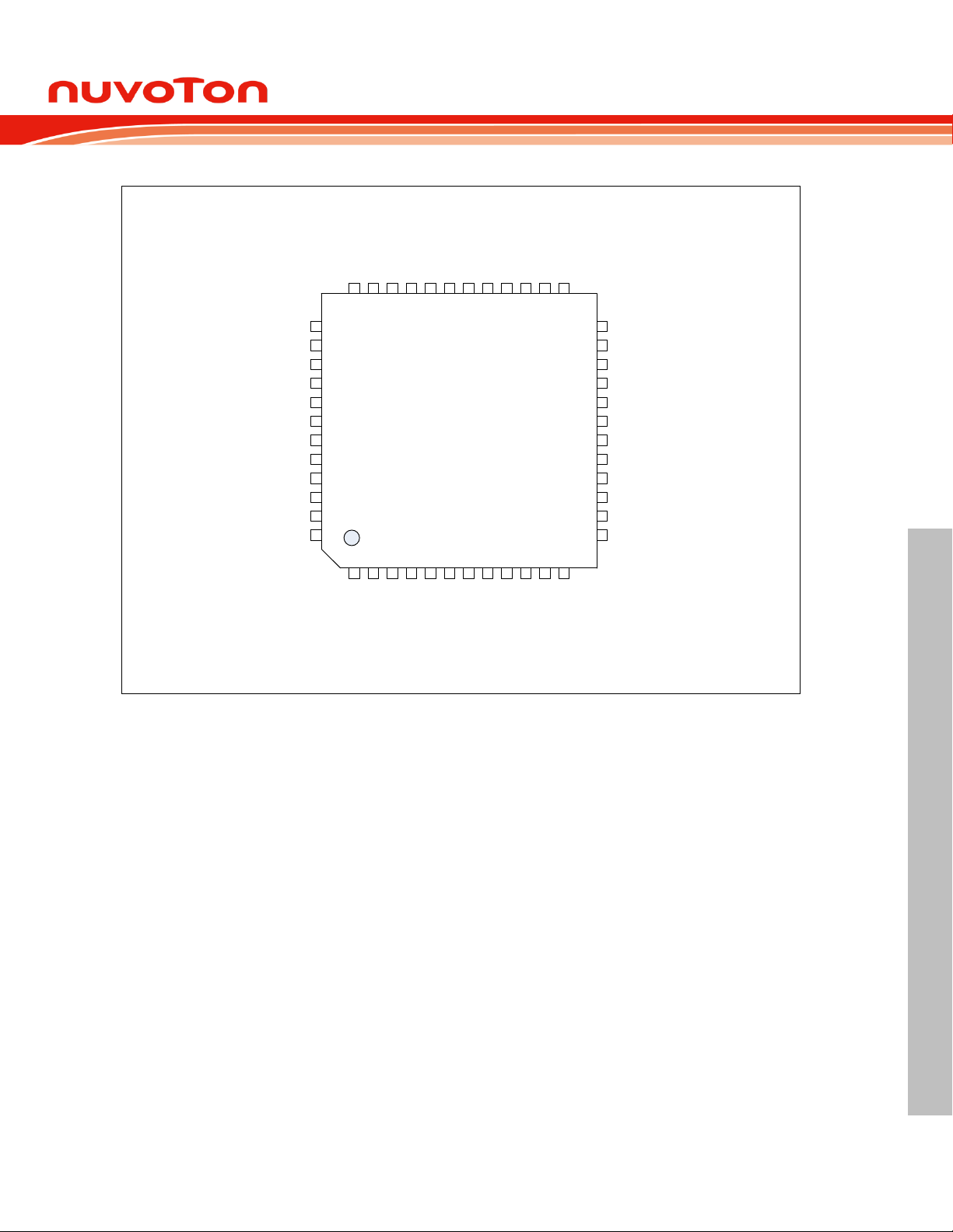
Figure 4.3-2 NuMicro® NUC029LEE LQFP 48-pin Diagram .......................................................... 21
Figure 5.1-1 NuMicro® NUC029LEE/NUC029SEE Block Diagram ............................................... 27
Figure 6.1-1 Functional Controller Diagram ................................................................................... 28
Figure 6.2-1 NuMicro® NUC029LEE/NUC029SEE Power Distribution Diagram ........................... 31
Figure 6.3-1 Clock Generator Block Diagram .............................................................................. 114
Figure 6.3-2 Clock Generator Global View Diagram.................................................................... 115
Figure 6.3-3 System Clock Block Diagram .................................................................................. 116
Figure 6.3-4 SysTick Clock Control Block Diagram ..................................................................... 116
Figure 6.3-5 Clock Source of Frequency Divider ......................................................................... 117
Figure 6.3-6 Frequency Divider Block Diagram ........................................................................... 118
Figure 6.4-1 Flash Memory Control Block Diagram ..................................................................... 143
Figure 6.4-2 Flash Memory Organization .................................................................................... 145
Figure 6.4-3 Program Executing Range for Booting from APROM and LDROM ........................ 149
Figure 6.4-4 Executable Range of Code with IAP Function Enabled .......................................... 150
Figure 6.4-5 Example Flow of Boot Selection by BS Bit .............................................................. 151
Figure 6.4-6 ISP Flow Example ................................................................................................... 152
Figure 6.5-1 EBI Block Diagram.................................................................................................. 165
Figure 6.5-2 Connection of 16-bit EBI Data Width with 16-bit Device ........................................ 166
Figure 6.5-3 Connection of 8-bit EBI Data Width with 8-bit Device ............................................. 166
Figure 6.5-4 Timing Control Waveform for 16-bit Data Width ...................................................... 168
Figure 6.5-5 Timing Control Waveform for 8-bit Data Width ....................................................... 169
Figure 6.5-6 Timing Control Waveform for Insert Idle Cycle ........................................................ 170
Figure 6.6-1 Push-Pull Output...................................................................................................... 177
Figure 6.6-2 Open-Drain Output .................................................................................................. 178
Figure 6.6-3 Quasi-bidirectional I/O Mode ................................................................................... 178
Figure 6.7-1 DMA Controller Block Diagram ................................................................................ 196
Figure 6.7-2 CRC Generator Block Diagram ............................................................................... 197
Figure 6.8-1 Timer Controller Block Diagram .............................................................................. 234
Figure 6.8-2 Clock Source of Timer Controller ............................................................................ 235
Figure 6.8-3 Continuous Counting Mode ..................................................................................... 237
Figure 6.9-1 PWM Generator 0 Clock Source Control................................................................. 252
Figure 6.9-2 PWM Generator 0 Architecture Diagram ................................................................. 252
Figure 6.9-3 PWM Generator 2 Clock Source Control................................................................. 253
Figure 6.9-4 PWM Generator 2 Architecture Diagram ................................................................. 253
Aug, 2018 Page 7 of 497 Rev 1.00
Page 8

NuMicro® NUC029LEE/NUC029SEE
NUMICRO
®
NUC029LEE/NUC029SEE TECHNICAL REFERENCE MANUAL
32-bit Arm® Cortex®-M0 Microcontroller
Figure 6.9-5 PWM Generator 4 Clock Source Control................................................................. 254
Figure 6.9-6 PWM Generator 4 Architecture Diagram ................................................................. 254
Figure 6.9-7 Legend of Internal Comparator Output of PWM-Timer ........................................... 255
Figure 6.9-8 PWM-Timer Operation Timing ................................................................................. 256
Figure 6.9-9 PWM Edge-aligned Interrupt Generate Timing Waveform ...................................... 256
Figure 6.9-10 Center-aligned Type Output Waveform ................................................................. 257
Figure 6.9-11 PWM Center-aligned Interrupt Generate Timing Waveform ................................. 258
Figure 6.9-12 PWM Double Buffering Illustration......................................................................... 259
Figure 6.9-13 PWM Controller Output Duty Ratio ........................................................................ 259
Figure 6.9-14 Paired-PWM Output with Dead-zone Generation Operation ................................ 260
Figure 6.9-15 PWM trigger ADC to conversion in Center-aligned type Timing Waveform .......... 260
Figure 6.9-16 Capture Operation Timing ..................................................................................... 261
Figure 6.9-17 PWM Group A PWM-Timer Interrupt Architecture Diagram .................................. 262
Figure 6.9-18 PWM Group B PWM-Timer Interrupt Architecture Diagram .................................. 262
Figure 6.10-1 Watchdog Timer Clock Control .............................................................................. 296
Figure 6.10-2 Watchdog Timer Block Diagram ............................................................................ 296
Figure 6.10-3 Watchdog Timer Time-out Interval and Reset Period Timing ............................... 298
Figure 6.11-1 Window Watchdog Timer Clock Control ................................................................ 303
Figure 6.11-2 Window Watchdog Timer Block Diagram .............................................................. 304
Figure 6.11-3 Window Watchdog Timer Reset and Reload Behavior ......................................... 305
Figure 6.12-1 RTC Block Diagram ............................................................................................... 314
Figure 6.13-1 UART Clock Control Diagram ................................................................................ 337
Figure 6.13-2 UART Block Diagram ............................................................................................ 338
Figure 6.13-3 Transmit Delay Time Operation ............................................................................. 341
Figure 6.13-4 Auto Flow Control Block Diagram .......................................................................... 345
Figure 6.13-5 UART CTS Auto Flow Control Enabled ................................................................. 345
Figure 6.13-6 UART RTS Auto Flow Control Enabled ................................................................. 346
Figure 6.13-7 UART RTS Flow with Software Control ................................................................ 346
Figure 6.13-8 IrDA Control Block Diagram .................................................................................. 347
Figure 6.13-9 IrDA TX/RX Timing Diagram ................................................................................. 348
Figure 6.13-10 Structure of LIN Frame ........................................................................................ 348
Figure 6.13-11 Structure of LIN Byte ........................................................................................... 349
Figure 6.13-12 Break Detection in LIN Mode ............................................................................... 351
Figure 6.13-13 LIN Frame ID and Parity Format ......................................................................... 352
Figure 6.13-14 LIN Sync Field Measurement .............................................................................. 354
Figure 6.13-15 UA_BAUD Update Sequence in Automatic Resynchronization Mode when
LINS_DUM_EN (UA_LIN_CTL[3]) = 1 .................................................................................. 355
Aug, 2018 Page 8 of 497 Rev 1.00
Page 9

NuMicro® NUC029LEE/NUC029SEE
NUMICRO
®
NUC029LEE/NUC029SEE TECHNICAL REFERENCE MANUAL
32-bit Arm® Cortex®-M0 Microcontroller
Figure 6.13-16 UA_BAUD Update Sequence in Automatic Resynchronization Mode when
LINS_DUM_EN (UA_LIN_CTL[3])= 0 ................................................................................... 355
Figure 6.13-17 RS-485 RTS Driving Level in Auto Direction Mode ............................................. 358
Figure 6.13-18 RS-485 RTS Driving Level with Software Control .............................................. 358
Figure 6.13-19 Structure of RS-485 Frame ................................................................................. 359
Figure 6.14-1 I2C Controller Block Diagram ................................................................................. 390
Figure 6.14-2 I2C Bus Timing ....................................................................................................... 391
Figure 6.14-3 I2C Protocol ........................................................................................................... 391
Figure 6.14-4 START and STOP Conditions ............................................................................... 392
Figure 6.14-5 Bit Transfer on the I2C Bus .................................................................................... 393
Figure 6.14-6 Acknowledge on the I2C Bus ................................................................................. 393
Figure 6.14-7 Master Transmits Data to Slave ............................................................................ 393
Figure 6.14-8 Master Reads Data from Slave ............................................................................. 394
Figure 6.14-9 Control I2C Bus according to Current I2C Status ................................................... 394
Figure 6.14-10 Master Transmitter Mode Control Flow ............................................................... 395
Figure 6.14-11 Master Receiver Mode Control Flow ................................................................... 396
Figure 6.14-12 Save Mode Control Flow ..................................................................................... 397
Figure 6.14-13 GC Mode ............................................................................................................. 398
Figure 6.14-14 Arbitration Lost..................................................................................................... 399
Figure 6.14-15 I2C Data Shifting Direction ................................................................................... 400
Figure 6.14-16 I2C Time-out Count Block Diagram ..................................................................... 402
Figure 6.14-17 EEPROM Random Read ..................................................................................... 403
Figure 6.14-18 Protocol of EEPROM Random Read .................................................................. 404
Figure 6.15-1 SPI Block Diagram................................................................................................. 417
Figure 6.15-2 SPI Master Mode Application Block Diagram ........................................................ 418
Figure 6.15-3 SPI Slave Mode Application Block Diagram .......................................................... 418
Figure 6.15-4 32-Bit in One Transaction ...................................................................................... 419
Figure 6.15-5 Variable Bus Clock Frequency .............................................................................. 421
Figure 6.15-6 Byte Reorder Function ........................................................................................... 421
Figure 6.15-7 Timing Waveform for Byte Suspend ...................................................................... 422
Figure 6.15-8 Bit Sequence of Dual Output Mode ....................................................................... 423
Figure 6.15-9 Bit Sequence of Dual Input Mode .......................................................................... 423
Figure 6.15-10 FIFO Mode Block Diagram .................................................................................. 424
Figure 6.15-11 SPI Timing in Master Mode ................................................................................. 426
Figure 6.15-12 SPI Timing in Master Mode (Alternate Phase of SPI Bus Clock) ........................ 426
Figure 6.15-13 SPI Timing in Slave Mode ................................................................................... 427
Figure 6.15-14 SPI Timing in Slave Mode (Alternate Phase of SPI Bus Clock) .......................... 427
Aug, 2018 Page 9 of 497 Rev 1.00
Page 10

NuMicro® NUC029LEE/NUC029SEE
NUMICRO
®
NUC029LEE/NUC029SEE TECHNICAL REFERENCE MANUAL
32-bit Arm® Cortex®-M0 Microcontroller
Figure 6.16-1 USB Device Block Diagram ................................................................................... 448
Figure 6.16-2 Wake-up Interrupt Operation Flow ....................................................................... 450
Figure 6.16-3 Endpoint SRAM Structure ..................................................................................... 451
Figure 6.16-4 Setup Transaction Followed by Data IN Transaction ............................................ 452
Figure 6.16-5 Data Out Transfer .................................................................................................. 452
Figure 6.17-1 ADC Controller Block Diagram .............................................................................. 473
Figure 6.17-2 ADC Clock Control................................................................................................. 474
Figure 6.17-3 Single Mode Conversion Timing Diagram ............................................................. 475
Figure 6.17-4 Single-Cycle Scan on Enabled Channels Timing Diagram ................................... 476
Figure 6.17-5 Continuous Scan on Enabled Channels Timing Diagram ..................................... 477
Figure 6.17-6 VBG for Measuring AVDD Application Block Diagram ............................................. 478
Figure 6.17-7 A/D Conversion Result Monitor Logics Diagram ................................................... 479
Figure 6.17-8 A/D Controller Interrupt .......................................................................................... 480
Figure 6.17-9 ADC Single-end Input Conversion Voltage and Conversion Result Mapping ....... 483
Figure 6.17-10 ADC Differential Input Conversion Voltage and Conversion Result Mapping ..... 484
Aug, 2018 Page 10 of 497 Rev 1.00
Page 11

NuMicro® NUC029LEE/NUC029SEE
NUMICRO
®
NUC029LEE/NUC029SEE TECHNICAL REFERENCE MANUAL
32-bit Arm® Cortex®-M0 Microcontroller
LIST OF TABLES
Table 4.1-1 List of Abbreviations.................................................................................................... 17
Table 6.2-1 Address Space Assignments for On-Chip Controllers ................................................ 33
Table 6.2-2 Exception Model ......................................................................................................... 80
Table 6.2-3 System Interrupt Map ................................................................................................. 81
Table 6.2-4 Vector Table Format ................................................................................................... 81
Table 6.3-1 Chip Idle/Power-down Mode Control Table .............................................................. 123
Table 6.4-1 Memory Address Map ............................................................................................... 144
Table 6.4-2 ISP Command List .................................................................................................... 153
Table 6.10-1 Watchdog Timer Time-out Interval Period Selection .............................................. 298
Table 6.11-1 Window Watchdog Timer Prescale Value Selection .............................................. 304
Table 6.11-2 WINCMP Setting Limitation .................................................................................... 306
Table 6.13-1 UART Interface Controller Pin ................................................................................ 339
Table 6.13-2 UART Baud Rate Equation ..................................................................................... 339
Table 6.13-3 UART Controller Baud Rate Parameter Setting Table ........................................... 340
Table 6.13-4 UART Controller Baud Rate Register (UA_BAUD) Setting Table .......................... 341
Table 6.13-5 UART Controller Interrupt Source and Flag List ..................................................... 343
Table 6.13-6 Controller Interrupt Source and Flag in DMA Mode List ......................................... 343
Table 6.13-7 UART Line Control of Word and Stop Length Setting ............................................ 344
Table 6.13-8 UART Line Control of Parity Bit Setting .................................................................. 344
Table 6.13-9 LIN Header Selection in Master Mode .................................................................... 349
Table 6.14-1 I2C Status Code Description ................................................................................... 402
Aug, 2018 Page 11 of 497 Rev 1.00
Page 12

NuMicro® NUC029LEE/NUC029SEE
NUMICRO
®
NUC029LEE/NUC029SEE TECHNICAL REFERENCE MANUAL
32-bit Arm® Cortex®-M0 Microcontroller
1 GENERAL DESCRIPTION
The NuMicro® NUC029LEE/NUC029SEE of NUC029 series is embedded with the ARM® Cortex®M0 core running up to 72 MHz and features 128 Kbytes flash, 16K bytes SRAM, and 8 Kbytes
loader ROM for the ISP. It is also equipped with plenty of peripheral devices, such as Timers,
Watchdog Timer, Window Watchdog Timer, RTC, PDMA with CRC calculation unit, UART, SPI,
I2C, PWM Timer, GPIO, LIN, CAN, USB 2.0 FS Device, 12-bit ADC, Low Voltage Reset Controller
and Brown-out Detector.
Aug, 2018 Page 12 of 497 Rev 1.00
Page 13

NUMICRO
®
NUC029LEE/NUC029SEE TECHNICAL REFERENCE MANUAL
NuMicro® NUC029LEE/NUC029SEE
32-bit Arm® Cortex®-M0 Microcontroller
2 FEATURES
ARM® Cortex®-M0 core
– Runs up to 72 MHz
– One 24-bit system timer
– Supports low power sleep mode
– Single-cycle 32-bit hardware multiplier
– NVIC for the 32 interrupt inputs, each with 4-levels of priority
– Serial Wire Debug supports with 2 watchpoints/4 breakpoints
Built-in LDO for wide operating voltage ranges from 2.5 V to 5.5 V
Flash Memory
– 128K bytes Flash for program code
– 8 KB flash for ISP loader
– Supports In-System-Program (ISP) and In-Application-Program (IAP) application code
update
– 512 byte page erase for flash
– Configurable Data Flash address and size for 128 KB system
– Supports 2-wired ICP update through SWD/ICE interface
SRAM Memory
– 16K bytes embedded SRAM
– Supports PDMA mode
PDMA (Peripheral DMA)
– Supports 9 channels PDMA for automatic data transfer between SRAM and peripherals
– Supports CRC calculation with four common polynomials, CRC-CCITT, CRC-8, CRC-16 and
CRC-32
Clock Control
– Flexible selection for different applications
– Built-in 22.1184 MHz high speed oscillator for system operation
Trimmed to ±1 % at +25 ℃ and VDD = 5 V
Trimmed to ±3 % at -40 ℃ ~ +105 ℃ and VDD = 2.5 V ~ 5.5 V
– Built-in 48 MHz internal high speed RC oscillator (HIRC) for USB device operation
(Frequency variation < 2% at -40oC ~ +105oC)
Dynamically calibrating the HIRC OSC to 48 MHz ±0.25% from -40℃ to 105℃ by
external 32.768K crystal oscillator (LXT) or internal USB synchronous mode
– Built-in 10 kHz low speed oscillator for Watchdog Timer and Wake-up operation
– Supports one PLL, up to 72 MHz, for high performance system operation
– External 4~24 MHz high speed crystal input for USB and precise timing operation
– External 32.768 kHz low speed crystal input for RTC function and low power system
operation
GPIO
– Four I/O modes:
Quasi-bidirectional
Push-pull output
Open-drain output
Input only with high impendence
– TTL/Schmitt trigger input selectable
– I/O pin configured as interrupt source with edge/level setting
Timer
– Supports 4 sets of 32-bit timers with 24-bit up-timer and one 8-bit prescale counter
– Independent clock source for each timer
– Provides one-shot, periodic, toggle and continuous counting operation modes
– Supports event counting function
– Supports input capture function
Watchdog Timer
– Multiple clock sources
Aug, 2018 Page 13 of 497 Rev 1.00
Page 14

NUMICRO
®
NUC029LEE/NUC029SEE TECHNICAL REFERENCE MANUAL
NuMicro® NUC029LEE/NUC029SEE
32-bit Arm® Cortex®-M0 Microcontroller
– 8 selectable time-out period from 1.6 ms ~ 26.0 sec (depending on clock source)
– Wake-up from Power-down or Idle mode
– Interrupt or reset selectable on watchdog time-out
– Supports 4 selectable Watchdog Timer reset delay period(1026, 130, 18 or 3 WDT_CLK)
Window Watchdog Timer
– 6-bit down counter with 11-bit prescale for wide range window selected
RTC
– Supports software compensation by setting frequency compensate register (FCR)
– Supports RTC counter (second, minute, hour) and calendar counter (day, month, year)
– Supports Alarm registers (second, minute, hour, day, month, year)
– Selectable 12-hour or 24-hour mode
– Automatic leap year recognition
– Supports periodic time tick interrupt with 8 period options 1/128, 1/64, 1/32, 1/16, 1/8, 1/4,
1/2 and 1 second
– Supports battery power pin (V
– Supports wake-up function
PWM/Capture
– Up to three built-in 16-bit PWM generators providing six PWM outputs or three
complementary paired PWM outputs
– Each PWM generator equipped with one clock source selector, one clock divider, one 8-bit
prescaler and one Dead-Zone generator for complementary paired PWM
– Supports One-shot or Auto-reload mode
– Up to six 16-bit digital capture timers (shared with PWM timers) providing six rising/falling
capture inputs
– Supports Capture interrupt
UART
– Up to three UART controllers
– UART ports with flow control (TXD, RXD, nCTS and nRTS)
– UART0 with 64-byte FIFO is for high speed
– UART1/2(optional) with 16-byte FIFO for standard device
– Supports IrDA (SIR) and LIN function
– Supports RS-485 9-bit mode and direction control
– Programmable baud-rate generator up to 1/16 system clock
– Supports CTS wake-up function (UART0 and UART1 support)
– Supports PDMA mode
SPI
– Up to two sets of SPI controllers
– The maximum SPI clock rate of Master can up to 36 MHz (chip working at 5V)
– The maximum SPI clock rate of Slave can up to 18 MHz (chip working at 5V)
– Supports SPI Master/Slave mode
– Full duplex synchronous serial data transfer
– Variable length of transfer data from 8 to 32 bits
– MSB or LSB first data transfer
– Rx and Tx on both rising or falling edge of serial clock independently
– Two slave/device select lines in Master mode, and one slave/device select line in Slave
mode
– Supports Byte Suspend mode in 32-bit transmission
– Supports PDMA mode
– Supports three wire, no slave select signal, bi-direction interface
I2C
– Up to two sets of I2C devices
– Master/Slave mode
– Bidirectional data transfer between masters and slaves
– Multi-master bus (no central master)
– Arbitration between simultaneously transmitting masters without corruption of serial data on
BAT
)
Aug, 2018 Page 14 of 497 Rev 1.00
Page 15

NUMICRO
®
NUC029LEE/NUC029SEE TECHNICAL REFERENCE MANUAL
NuMicro® NUC029LEE/NUC029SEE
32-bit Arm® Cortex®-M0 Microcontroller
the bus
– Serial clock synchronization allowing devices with different bit rates to communicate via one
serial bus
– Serial clock synchronization used as a handshake mechanism to suspend and resume serial
transfer
– Programmable clocks allowing for versatile rate control
– Supports multiple address recognition (four slave address with mask option)
– Supports wake-up function
USB 2.0 Full-Speed Device
– One set of USB 2.0 FS Device 12 Mbps
– On-chip USB Transceiver
– Provides 1 interrupt source with 4 interrupt events
– Supports Control, Bulk In/Out, Interrupt and Isochronous transfers
– Auto suspend function when no bus signaling for 3 ms
– Provides 8 programmable endpoints
– Includes 512 Bytes internal SRAM as USB buffer
– Provides remote wake-up capability
– Supports Crystal-less function
ADC
– 12-bit SAR ADC with 1 MSPS(chip working at 5V)
– Up to 12-ch single-end input or 5-ch differential input
– Single scan/single cycle scan/continuous scan
– Each channel with individual result register
– Scan on enabled channels
– Threshold voltage detection
– Conversion started by software programming, external input or PWM Center-aligned trigger
– Supports PDMA mode
EBI (External bus interface)
– Accessible space: 64 KB in 8-bit mode or 128 KB in 16-bit mode
– Supports 8-/16-bit data width
– Supports byte write in 16-bit data width mode
96-bit unique ID (UID)
128-bit unique customer ID(UCID)
One built-in temperature sensor with 1℃ resolution
Brown-out Detector
– With 4 levels: 4.4 V/3.7 V/2.7 V/2.2 V
– Supports Brown-out Interrupt and Reset option
Low Voltage Reset
– Threshold voltage level: 2.0 V
Operating Temperature: -40℃ ~ 105℃
Packages:
– All Green package (RoHS)
– LQFP 64-pin / 48-pin
Aug, 2018 Page 15 of 497 Rev 1.00
Page 16
NUMICRO
®
NUC029LEE/NUC029SEE TECHNICAL REFERENCE MANUAL
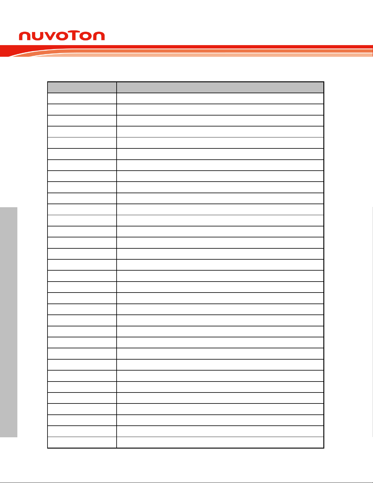
3 ABBREVIATIONS
Acronym
Description
ACMP
Analog Comparator Controller
ADC
Analog-to-Digital Converter
AES
Advanced Encryption Standard
APB
Advanced Peripheral Bus
AHB
Advanced High-Performance Bus
BOD
Brown-out Detection
CAN
Controller Area Network
DAP
Debug Access Port
DES
Data Encryption Standard
EBI
External Bus Interface
EPWM
Enhanced Pulse Width Modulation
FIFO
First In, First Out
FMC
Flash Memory Controller
FPU
Floating-point Unit
GPIO
General-Purpose Input/Output
HCLK
The Clock of Advanced High-Performance Bus
HIRC
22.1184 MHz Internal High Speed RC Oscillator
HXT
4~24 MHz External High Speed Crystal Oscillator
IAP
In Application Programming
ICP
In Circuit Programming
ISP
In System Programming
LDO
Low Dropout Regulator
LIN
Local Interconnect Network
LIRC
10 kHz internal low speed RC oscillator (LIRC)
MPU
Memory Protection Unit
NVIC
Nested Vectored Interrupt Controller
PCLK
The Clock of Advanced Peripheral Bus
PDMA
Peripheral Direct Memory Access
PLL
Phase-Locked Loop
PWM
Pulse Width Modulation
QEI
Quadrature Encoder Interface
SDIO
Secure Digital Input/Output
NuMicro® NUC029LEE/NUC029SEE
32-bit Arm® Cortex®-M0 Microcontroller
Aug, 2018 Page 16 of 497 Rev 1.00
Page 17
NuMicro® NUC029LEE/NUC029SEE
NUMICRO
®
NUC029LEE/NUC029SEE TECHNICAL REFERENCE MANUAL
SPI
Serial Peripheral Interface
SPS
Samples per Second
TDES
Triple Data Encryption Standard
TMR
Timer Controller
UART
Universal Asynchronous Receiver/Transmitter
UCID
Unique Customer ID
USB
Universal Serial Bus
WDT
Watchdog Timer
WWDT
Window Watchdog Timer
32-bit Arm® Cortex®-M0 Microcontroller
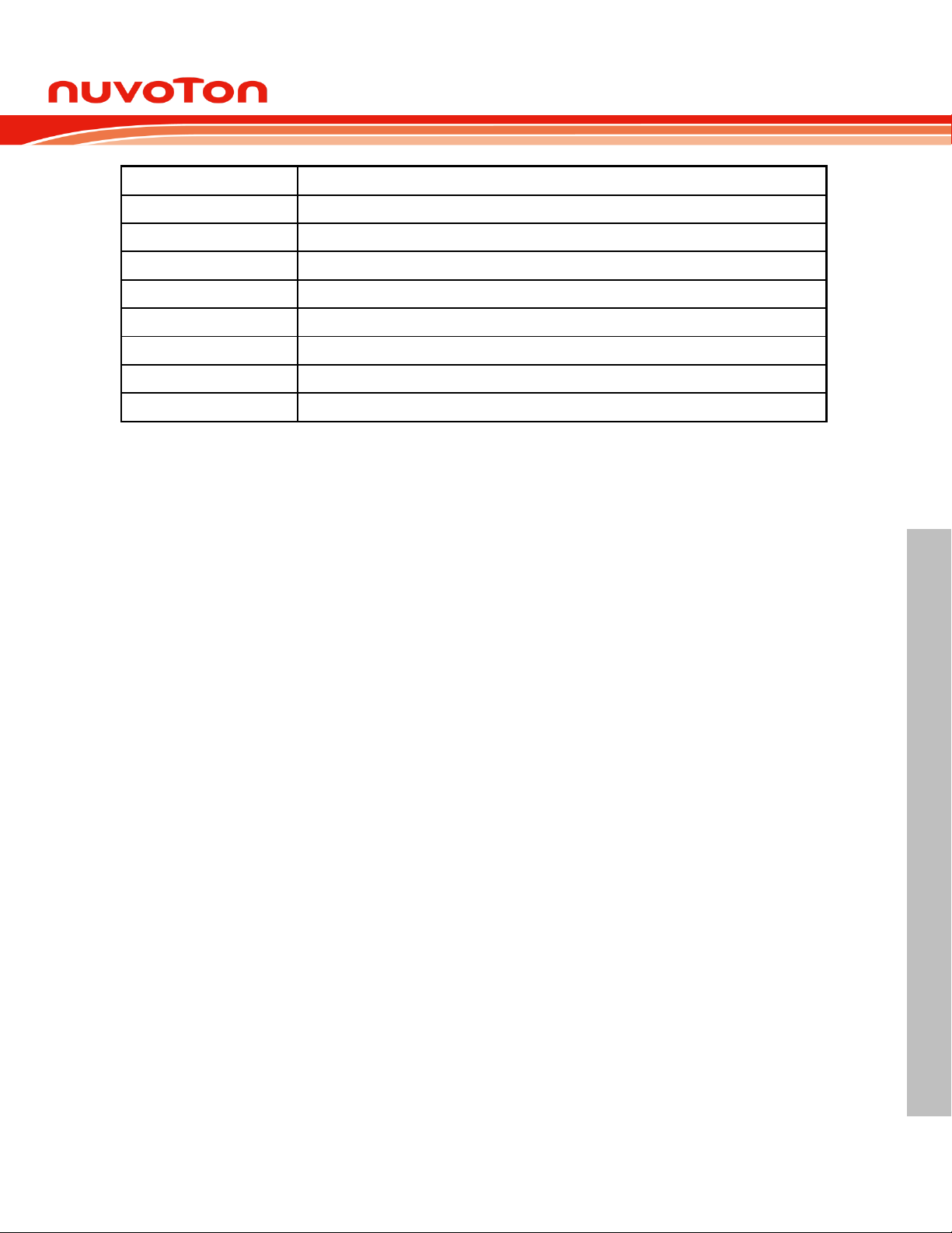
Table 4.1-1 List of Abbreviations
Aug, 2018 Page 17 of 497 Rev 1.00
Page 18
NuMicro® NUC029LEE/NUC029SEE
NUMICRO
®
NUC029LEE/NUC029SEE TECHNICAL REFERENCE MANUAL
CPU core
ARM Cortex M0
Package Type
F: TSSOP 20
T: QFN33 (5x5)
Z: QFN33 (4x4)
N: QFN48 (7x7)
L: LQFP 48 (7x7)
S: LQFP 64 (7x7)
Temperature
Flash Size
A: Less than 68K
D: 68K
E: 128K
G: 256K
NUC029
-
X
XX
E: - 40 ℃ ~ +105℃
N: - 40 ℃ ~ +85℃
32-bit Arm® Cortex®-M0 Microcontroller
4 PARTS INFORMATION LIST AND PIN CONFIGURATION
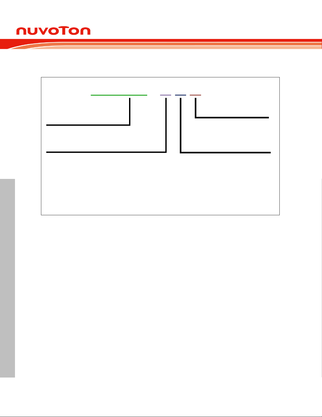
4.1 NuMicro® NUC029 Series Selection Code
Aug, 2018 Page 18 of 497 Rev 1.00
Figure 4.1-1 NuMicro® NUC029 Series Selection Code
Page 19
32-bit Arm® Cortex®-M0 Microcontroller
NUMICRO
®
NUC029LEE/NUC029SEE TECHNICAL REFERENCE MANUAL
Part Number
APROM (KB)
RAM (KB)
Data Flash (KB)
SPROM(KB)
ISP ROM (KB)
I/O
Timer (32-Bit)
Connectivity
I
2
S
PWM (16-Bit)
ADC
ACMP
PDMA
RTC
EBI
PLL
ISP/ICP/IAP
Package
Operating
Temperature
Range (℃)
UART
SPI
I
2
C
USCI
[4]
USB
LIN
NUC029FAE
16 2 Conf - 2
17 2 1 1 1 - - - - 3 4
[1] 2[3]
- - - - √ TSSOP20
-40 to +105
NUC029TAN
32 4 4 - 4
24 4 2 1 2 - - - - 5 5
3
[2]
- - - √ √ QFN33(4*4)
-40 to +85
NUC029ZAN
64 4 4 - 4
24 4 2 1 2 - - - - 5 5
3
[2]
- - - √ √
QFN33(5*5)
-40 to +85
NUC029LAN
64 4 4 - 4
40 4 2 2 2 - - - - 8 8 4 - - √ √ √
LQFP48
-40 to +85
NUC029LDE
68 8 Conf - 4
42 4 4 1 2 - - 3 -
12 8 - - - - √ √ LQFP48
-40 to +105
NUC029SDE
68 8 Conf - 4
56 4 4 1 2 - - 3 -
12 8 - - - - √ √ LQFP64
-40 to +105
NUC029LEE
128
16
Conf - 8
31 4 2 1 2 - 1 2 - 6 10 - 9 √ - √ √
LQFP48
-40 to +105
NUC029SEE
128
16
Conf - 8
45 4 3 2 2 - 1 3 - 6 12 - 9 √ √ √ √
LQFP64
-40 to +105
NUC029LGE
256
20
Conf 2 4
35 4 3 2 2 3 1 - 2
10 9 2 5 √ √ √ √ LQFP48
-40 to +105
NUC029SGE
256
20
Conf 2 4
49 4 3 2 2 3 1 - 2
12
15 2 5 √ √ √ √
LQFP64
-40 to +105
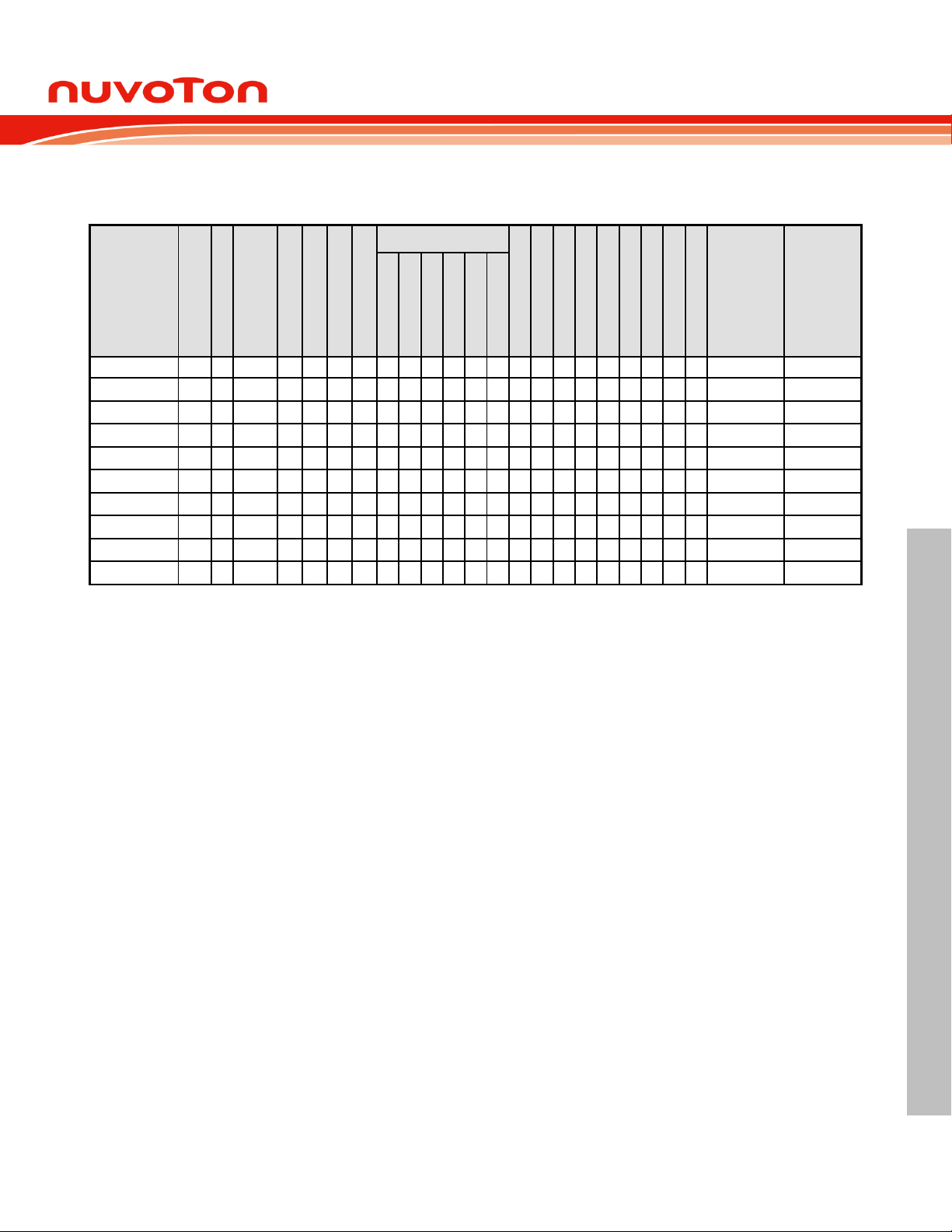
4.2 NuMicro® NUC029 Series Selection Guide
NuMicro® NUC029LEE/NUC029SEE
[1] NUC029FAE is 10-bit ADC. All the others are 12-bit ADC.
[2] For NUC029TAN/NUC029ZAN, ACMP3 only has positive and negative input.
[3] For NUC029FAE , ACMP0 only has positive and negative input. And ACMP1 only has positive input.
[4] USCI 能够被配置为 UART, SPI 或 I2C
Aug, 2018 Page 19 of 497 Rev 1.00
Page 20
NuMicro® NUC029LEE/NUC029SEE
NUMICRO
®
NUC029LEE/NUC029SEE TECHNICAL REFERENCE MANUAL
AD8/ADC5/PA.5
AD7/ADC6/PA.6
V
REF
AD0/INT0/PB.14
AD1/PB.13
V
BAT
X32_IN
X32_OUT
nRD/I2C1_SCL/PA.11
nWR/I2C1_SDA/PA.10
I2C0_SCL/PA.9
I2C0_SDA/PA.8
UART1_RXD/PB.4
UART1_TXD/PB.5
ALE/UART1_nRTS/PB.6
nCS/UART1_nCTS/PB.7
LDO_CAP
V
DD
V
SS
AD5/ADC7/PC.7
AD4/ADC8/PC.6
AD3/ADC9/PC.15
AD2/ADC10/PC.14
AD6/ADC11/TM0/TM0_EXT/INT1/PB.15
XT1_OUT/PF.0
XT1_IN/PF.1
nRESET
CLKO/TM0/STADC/PB.8
PA.4/ADC4/AD9
PA.3/ADC3/AD10
PA.2/ADC2/AD11
PA.1/ADC1/AD12
PA.0/ADC0
AVSSICE_CLK
ICE_DAT
PA.12/PWM0/AD13
PA.13/PWM1/AD14
PA.14/PWM2/AD15
PA.15/PWM3
PC.8/SPI1_SS0/MCLK
PC.9/SPI1_CLK
AV
DD
V
SS
V
DD
PV
SS
PC.0/SPI0_SS0
PC.1/SPI0_CLK
PC.2/SPI0_MISO0
PC.3/SPI0_MOSI0
USB_D+
USB_D-
USB_VDD33_CAP
USB_VBUS17
18
19
20
21
22
23
24
25
26
27
28
29
30
31
32
64
63
62
61
60
59
58
57
56
55
54
53
52
51
50
49
16
15
14
13
12
11
10
9
8
7
6
5
4
3
2
1
33
34
35
36
37
38
39
40
41
42
43
44
45
46
47
48
PC.10/SPI1_MISO0
PC.11/SPI1_MOSI0
PB.9/TM1/UART2_TXD
PB.10/TM2/UART2_RXD
PB.11/TM3/PWM4
PE.5/TM1_EXT/TM1/PWM5
PB.3/UART0_nCTS/TM3_EXT/TM3/nWRH
PB.2/UART0_nRTS/TM2_EXT/TM2/nWRL
PB.1/UART0_TXD
PB.0/UART0_RXD
NUC029SEE
LQFP 64-pin
32-bit Arm® Cortex®-M0 Microcontroller
4.3 Pin Configuration
4.3.1 NuMicro® NUC029LEE/NUC029SEE Pin Diagram
4.3.1.1 NuMicro® NUC029SEE LQFP 64 pin (7 mm * 7mm)
Aug, 2018 Page 20 of 497 Rev 1.00
Figure 4.3-1 NuMicro® NUC029SEE LQFP 64-pin Diagram
Page 21
NuMicro® NUC029LEE/NUC029SEE
NUMICRO
®
NUC029LEE/NUC029SEE TECHNICAL REFERENCE MANUAL
ADC5/PA.5
ADC6/PA.6
V
REF
V
BAT
X32_IN
X32_OUT
I2C1_SCL/PA.11
I2C1_SDA/PA.10
I2C0_SCL/PA.9
I2C0_SDA/PA.8
UART1_RXD/PB.4
UART1_TXD/PB.5
LDO_CAP
V
DD
V
SS
ADC7/PC.7
ADC8/PC.6
ADC11/TM0/TM0_EXT/INT1/PB.15
XT1_OUT/PF.0
XT1_IN/PF.1
nRESET
CLKO/TM0/STADC/PB.8
PA.4/ADC4
PA.3/ADC3
PA.2/ADC2
PA.1/ADC1
PA.0/ADC0
AVSSICE_CLK
ICE_DAT
PA.12/PWM0
PA.13/PWM1
PA.14/PWM2
PA.15/PWM3
AV
DD
PV
SS
PC.0/SPI0_SS0
PC.1/SPI0_CLK
PC.2/SPI0_MISO0
PC.3/SPI0_MOSI0
PB.3/UART0_nCTS/TM3_EXT/TM3
PB.2/UART0_nRTS/TM2_EXT/TM2
PB.1/UART0_TXD
PB.0/UART0_RXD
USB_D+
USB_D-
USB_VDD33_CAP
USB_VBUS13
14
15
16
17
18
19
20
21
22
23
24
48
47
46
45
44
43
42
41
40
39
38
37
12
11
10
9
8
7
6
5
4
3
2
1
25
26
27
28
29
30
31
32
33
34
35
36
NUC029LEE
LQFP 48-pin
32-bit Arm® Cortex®-M0 Microcontroller
4.3.1.2 NuMicro® NUC029LEE LQFP 48 pin (7 mm * 7mm)
Figure 4.3-2 NuMicro® NUC029LEE LQFP 48-pin Diagram
Aug, 2018 Page 21 of 497 Rev 1.00
Page 22
NuMicro® NUC029LEE/NUC029SEE
NUMICRO
®
NUC029LEE/NUC029SEE TECHNICAL REFERENCE MANUAL
Pin No.
Pin Name
Pin
Type
Description
LQFP
64-pin
LQFP
48-pin
1
PB.14
I/O
General purpose digital I/O pin.
INT0 I External interrupt0 input pin.
AD0
I/O
EBI Address/Data bus bit0
2
PB.13
I/O
General purpose digital I/O pin.
AD1
I/O
EBI Address/Data bus bit1
3
1
V
BAT
P Power supply by batteries for RTC.
4
2
X32_OUT
O
External 32.768 kHz (low speed) crystal output pin.
5
3
X32_IN
I
External 32.768 kHz (low speed) crystal input pin.
6
4
PA.11
I/O
General purpose digital I/O pin.
I2C1_SCL
I/O
I2C1 clock pin.
nRD O EBI read enable output pin
7
5
PA.10
I/O
General purpose digital I/O pin.
I2C1_SDA
I/O
I2C1 data input/output pin.
nWR O EBI write enable output pin
8
6
PA.9
I/O
General purpose digital I/O pin.
I2C0_SCL
I/O
I2C0 clock pin.
9
7
PA.8
I/O
General purpose digital I/O pin.
I2C0_SDA
I/O
I2C0 data input/output pin.
10
8
PB.4
I/O
General purpose digital I/O pin.
UART1_RXD
I
Data receiver input pin for UART1.
11
9
PB.5
I/O
General purpose digital I/O pin.
UART1_TXD
O
Data transmitter output pin for UART1.
12
PB.6
I/O
General purpose digital I/O pin.
UART1_nRTS
O
Request to Send output pin for UART1.
ALE O EBI address latch enable output pin
13
PB.7
I/O
General purpose digital I/O pin.
UART1_nCTS
I
Clear to Send input pin for UART1.
32-bit Arm® Cortex®-M0 Microcontroller
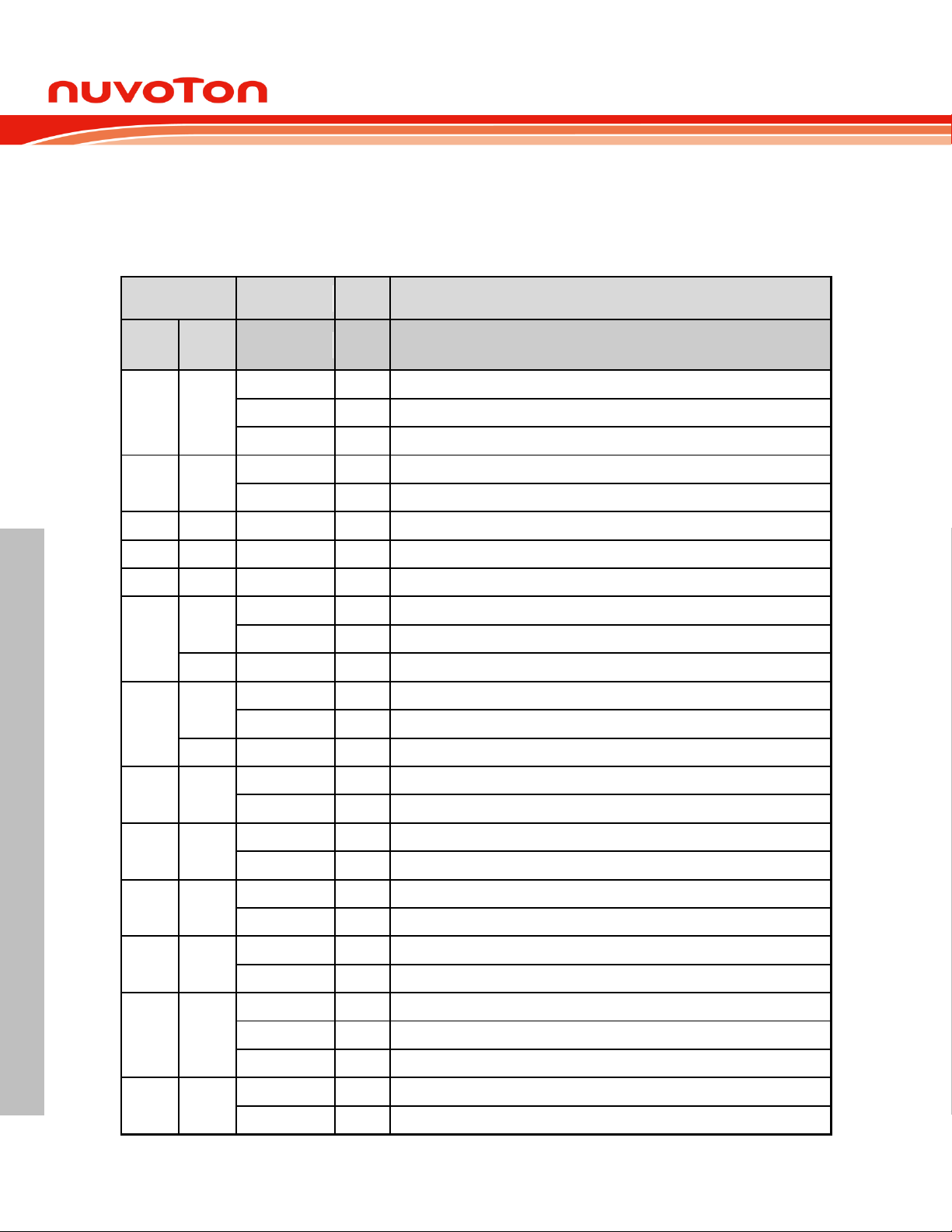
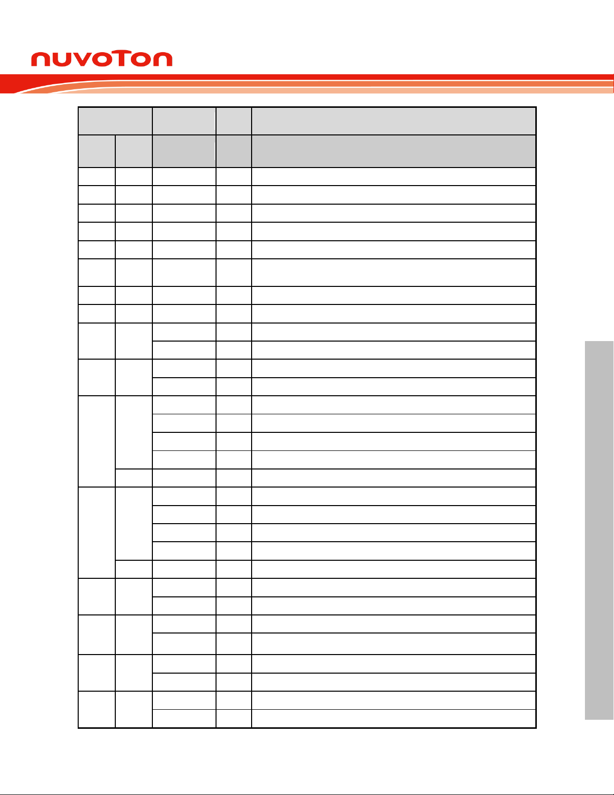
4.4 Pin Description
4.4.1 NuMicro® NUC029LEE/NUC029SEE Pin Description
Aug, 2018 Page 22 of 497 Rev 1.00
Page 23
NuMicro® NUC029LEE/NUC029SEE
NUMICRO
®
NUC029LEE/NUC029SEE TECHNICAL REFERENCE MANUAL
Pin No.
Pin Name
Pin
Type
Description
LQFP
64-pin
LQFP
48-pin
nCS O EBI chip select enable output pin
14
10
LDO_CAP
P
LDO output pin.
15
11
VDD P Power supply for I/O ports and LDO source for internal PLL and digital circuit.
16
12
VSS P Ground pin for digital circuit.
17
13
USB_VBUS
USB
Power supply from USB host or HUB.
18
14
USB_VDD33_C
AP
USB
Internal power regulator output 3.3V decoupling pin.
19
15
USB_D-
USB
USB differential signal D-.
20
16
USB_D+
USB
USB differential signal D+.
21
17
PB.0
I/O
General purpose digital I/O pin.
UART0_RXD
I
Data receiver input pin for UART0.
22
18
PB.1
I/O
General purpose digital I/O pin.
UART0_TXD
O
Data transmitter output pin for UART0.
23
19
PB.2
I/O
General purpose digital I/O pin.
UART0_nRTS
O
Request to Send output pin for UART0.
TM2_EXT
I
Timer2 external capture input pin.
TM2 O Timer2 toggle output pin.
nWRL
O
EBI low byte write enable output pin
24
20
PB.3
I/O
General purpose digital I/O pin.
UART0_nCTS
I
Clear to Send input pin for UART0.
TM3_EXT
I
Timer3 external capture input pin.
TM3 O Timer3 toggle output pin.
nWRH
O
EBI high byte write enable output pin
25
21
PC.3
I/O
General purpose digital I/O pin.
SPI0_MOSI0
I/O
1st SPI0 MOSI (Master Out, Slave In) pin.
26
22
PC.2
I/O
General purpose digital I/O pin.
SPI0_MISO0
I/O
1st SPI0 MISO (Master In, Slave Out) pin.
27
23
PC.1
I/O
General purpose digital I/O pin.
SPI0_CLK
I/O
SPI0 serial clock pin.
28
24
PC.0
I/O
General purpose digital I/O pin.
SPI0_SS0
I/O
1st SPI0 slave select pin.
32-bit Arm® Cortex®-M0 Microcontroller
Aug, 2018 Page 23 of 497 Rev 1.00
Page 24
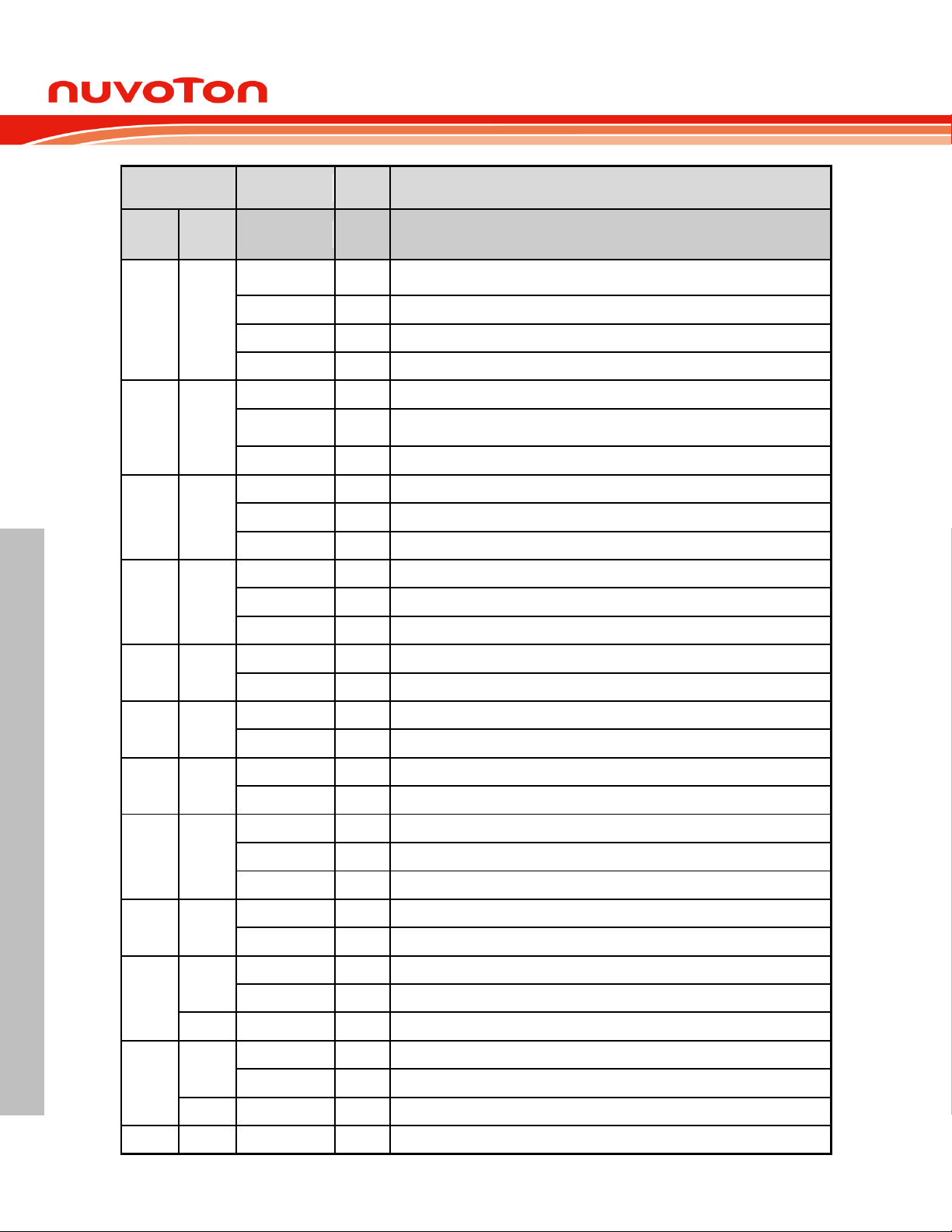
NuMicro® NUC029LEE/NUC029SEE
NUMICRO
®
NUC029LEE/NUC029SEE TECHNICAL REFERENCE MANUAL
Pin No.
Pin Name
Pin
Type
Description
LQFP
64-pin
LQFP
48-pin
29
PE.5
I/O
General purpose digital I/O pin.
PWM5
I/O
PWM5 output/Capture input.
TM1_EXT
I
Timer1 external capture input pin.
TM1 O Timer1 toggle output pin.
30
PB.11
I/O
General purpose digital I/O pin.
TM3
I/O
Timer3 event counter input / toggle output.
PWM4
I/O
PWM4 output/Capture input.
31
PB.10
I/O
General purpose digital I/O pin.
TM2
I/O
Timer2 event counter input / toggle output.
UART2_RXD
I
Data receiver input pin for UART2.
32
PB.9
I/O
General purpose digital I/O pin.
TM1
I/O
Timer1 event counter input / toggle output.
UART2_TXD
O
Data transmitter output pin for UART2.
33
PC.11
I/O
General purpose digital I/O pin.
SPI1_MOSI0
I/O
1st SPI1 MOSI (Master Out, Slave In) pin.
34
PC.10
I/O
General purpose digital I/O pin.
SPI1_MISO0
I/O
1st SPI1 MISO (Master In, Slave Out) pin.
35
PC.9
I/O
General purpose digital I/O pin.
SPI1_CLK
I/O
SPI1 serial clock pin.
36
PC.8
I/O
General purpose digital I/O pin.
SPI1_SS0
I/O
1st SPI1 slave select pin.
MCLK
O
EBI clock output
37
25
PA.15
I/O
General purpose digital I/O pin.
PWM3
I/O
PWM3 output/Capture input.
38
26
PA.14
I/O
General purpose digital I/O pin.
PWM2
I/O
PWM2 output/Capture input.
AD15
I/O
EBI Address/Data bus bit15
39
27
PA.13
I/O
General purpose digital I/O pin.
PWM1
I/O
PWM1 output/Capture input.
AD14
I/O
EBI Address/Data bus bit14
40
28
PA.12
I/O
General purpose digital I/O pin.
32-bit Arm® Cortex®-M0 Microcontroller
Aug, 2018 Page 24 of 497 Rev 1.00
Page 25
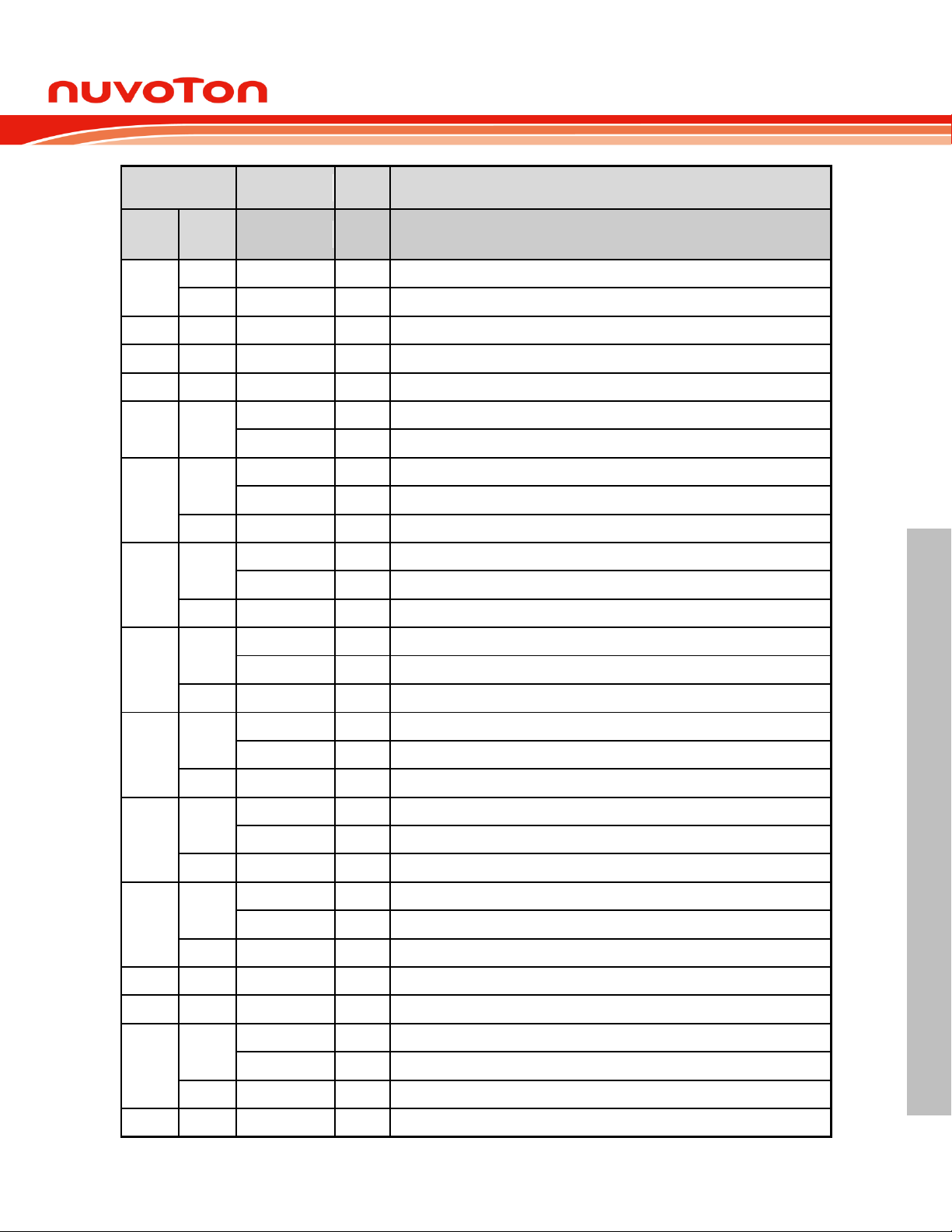
NuMicro® NUC029LEE/NUC029SEE
NUMICRO
®
NUC029LEE/NUC029SEE TECHNICAL REFERENCE MANUAL
Pin No.
Pin Name
Pin
Type
Description
LQFP
64-pin
LQFP
48-pin
PWM0
I/O
PWM0 output/Capture input.
AD13
I/O
EBI Address/Data bus bit13
41
29
ICE_DAT
I/O
Serial wire debugger data pin.
42
30
ICE_CLK
I
Serial wire debugger clock pin.
43
31
AVSS
AP
Ground pin for analog circuit.
44
32
PA.0
I/O
General purpose digital I/O pin.
ADC0
AI
ADC0 analog input.
45
33
PA.1
I/O
General purpose digital I/O pin.
ADC1
AI
ADC1 analog input.
AD12
I/O
EBI Address/Data bus bit12
46
34
PA.2
I/O
General purpose digital I/O pin.
ADC2
AI
ADC2 analog input.
AD11
I/O
EBI Address/Data bus bit11
47
35
PA.3
I/O
General purpose digital I/O pin.
ADC3
AI
ADC3 analog input.
AD10
I/O
EBI Address/Data bus bit10
48
36
PA.4
I/O
General purpose digital I/O pin.
ADC4
AI
ADC4 analog input.
AD9
I/O
EBI Address/Data bus bit9
49
37
PA.5
I/O
General purpose digital I/O pin.
ADC5
AI
ADC5 analog input.
AD8
I/O
EBI Address/Data bus bit8
50
38
PA.6
I/O
General purpose digital I/O pin.
ADC6
AI
ADC6 analog input.
AD7
I/O
EBI Address/Data bus bit7
51
39
V
REF
AP
Voltage reference input for ADC.
52
40
AVDD
AP
Power supply for internal analog circuit.
53
41
PC.7
I/O
General purpose digital I/O pin.
ADC7
AI
ADC7 analog input.
AD5
I/O
EBI Address/Data bus bit5
54
42
PC.6
I/O
General purpose digital I/O pin.
32-bit Arm® Cortex®-M0 Microcontroller
Aug, 2018 Page 25 of 497 Rev 1.00
Page 26
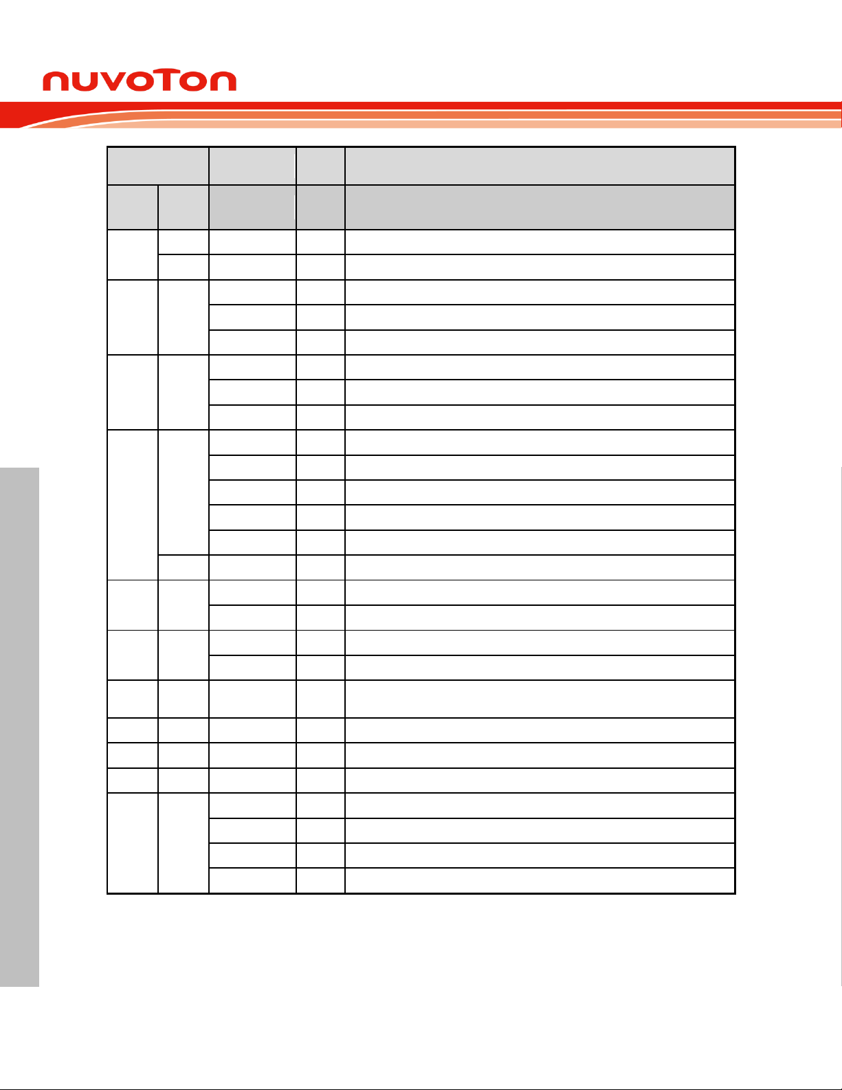
NuMicro® NUC029LEE/NUC029SEE
NUMICRO
®
NUC029LEE/NUC029SEE TECHNICAL REFERENCE MANUAL
Pin No.
Pin Name
Pin
Type
Description
LQFP
64-pin
LQFP
48-pin
ADC8
AI
ADC8 analog input.
AD4
I/O
EBI Address/Data bus bit4
55
PC.15
I/O
General purpose digital I/O pin.
ADC9
AI
ADC9 analog input.
AD3
I/O
EBI Address/Data bus bit3
56
PC.14
I/O
General purpose digital I/O pin.
ADC10
AI
ADC10 analog input.
AD2
I/O
EBI Address/Data bus bit2
57
43
PB.15
I/O
General purpose digital I/O pin.
INT1 I External interrupt1 input pin.
TM0_EXT
I
Timer 0 external capture input pin.
TM0
I/O
Timer0 event counter input / toggle output.
ADC11
AI
ADC11 analog input.
AD6
I/O
EBI Address/Data bus bit6
58
44
PF.0
I/O
General purpose digital I/O pin.
XT1_OUT
O
External 4~24 MHz (high speed) crystal output pin.
59
45
PF.1
I/O
General purpose digital I/O pin.
XT1_IN
I
External 4~24 MHz (high speed) crystal input pin.
60
46
nRESET
I
External reset input: active LOW, with an internal pull-up. Set this pin low reset
chip to initial state.
61
VSS P Ground pin for digital circuit.
62
VDD P Power supply for I/O ports and LDO source for internal PLL and digital circuit.
63
47
PVSS P PLL ground.
64
48
PB.8
I/O
General purpose digital I/O pin.
STADC
I
ADC external trigger input.
TM0
I/O
Timer0 event counter input / toggle output.
CLKO
O
Frequency divider clock output pin.
32-bit Arm® Cortex®-M0 Microcontroller
Note: Pin Type I = Digital Input, O = Digital Output; AI = Analog Input; P = Power Pin; AP = Analog Power
Aug, 2018 Page 26 of 497 Rev 1.00
Page 27
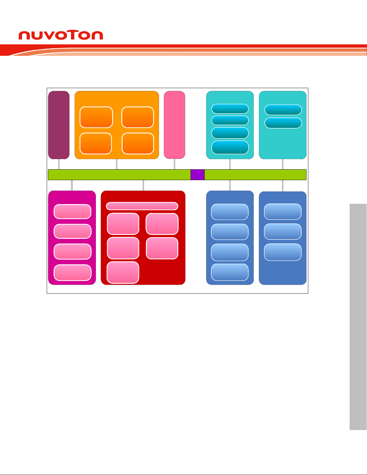
NuMicro® NUC029LEE/NUC029SEE
NUMICRO
®
NUC029LEE/NUC029SEE TECHNICAL REFERENCE MANUAL
ARM
Cortex-M0
72MHz
Memory
APROM
128 KB
DataFlash
Configurable
SRAM
16 KB
Timer/PWM Analog Interface
32-bit Timer x 4
RTC
PWM/Capture
Timer x 6
Watchdog Timer
12-bit ADC x 12
Power Control Clock Control
LDO
Power On Reset
LVR
Brownout
Detection
High Speed
Oscillator
48 MHz
High Speed
Crystal Osc.
4 ~ 24 MHz
High Speed
Oscillator
22.1184 MHz
PLL
Connectivity
I/O Ports
General Purpose
I/O
Reset Pin
External Interrupt
Low Speed
Crystal Osc.
32.768 KHz
LDROM
8 KB
USB PHY
AHB Bus APB Bus
Bridge
PDMA
UART x 3
I2C x 2
SPI x 2
USB
Low Speed
Oscillator
10 kHz
32-bit Arm® Cortex®-M0 Microcontroller
5 BLOCK DIAGRAM
5.1 NuMicro® NUC029LEE/NUC029SEE Block Diagram
Figure 5.1-1 NuMicro® NUC029LEE/NUC029SEE Block Diagram
Aug, 2018 Page 27 of 497 Rev 1.00
Page 28
NuMicro® NUC029LEE/NUC029SEE
NUMICRO
®
NUC029LEE/NUC029SEE TECHNICAL REFERENCE MANUAL
Cortex®-M0
Processor
Core
Nested
Vectored
Interrupt
Controller
(NVIC)
Breakpoint
and
Watchpoint
Unit
Debugger
Interface
Bus Matrix
Debug
Access
Port
(DAP)
Debug
Cortex®-M0 processor
Cortex®-M0 Components
Wakeup
Interrupt
Controller
(WIC)
Interrupts
Serial Wire or
JTAG Debug Port
AHB-Lite
Interface
32-bit Arm® Cortex®-M0 Microcontroller
6 FUNCTIONAL DESCRIPTION
6.1 ARM® Cortex®-M0 Core
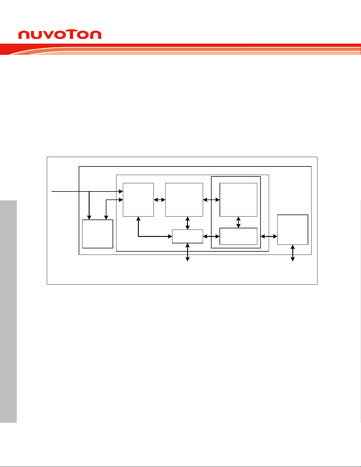
The Cortex®-M0 processor is a configurable, multistage, 32-bit RISC processor, which has an
AMBA AHB-Lite interface and includes an NVIC component. It also has optional hardware debug
functionality. The processor can execute Thumb code and is compatible with other Cortex®-M
profile processor. The profile supports two modes -Thread mode and Handler mode. Handler
mode is entered as a result of an exception. An exception return can only be issued in Handler
mode. Thread mode is entered on Reset, and can be entered as a result of an exception return.
Figure 6.1-1 shows the functional controller of processor.
The implemented device provides the following components and features:
A low gate count processor:
Figure 6.1-1 Functional Controller Diagram
- ARMv6-M Thumb® instruction set
- Thumb-2 technology
- ARMv6-M compliant 24-bit SysTick timer
- A 32-bit hardware multiplier
- System interface supported with little-endian data accesses
- Ability to have deterministic, fixed-latency, interrupt handling
- Load/store-multiples and multicycle-multiplies that can be abandoned and
restarted to facilitate rapid interrupt handling
- C Application Binary Interface compliant exception model. This is the ARMv6-M,
C Application Binary Interface (C-ABI) compliant exception model that enables
the use of pure C functions as interrupt handlers
- Low Power Sleep mode entry using Wait For Interrupt (WFI), Wait For Event
Aug, 2018 Page 28 of 497 Rev 1.00
Page 29

NuMicro® NUC029LEE/NUC029SEE
NUMICRO
®
NUC029LEE/NUC029SEE TECHNICAL REFERENCE MANUAL
32-bit Arm® Cortex®-M0 Microcontroller
(WFE) instructions, or the return from interrupt sleep-on-exit feature
NVIC:
- 32 external interrupt inputs, each with four levels of priority
- Dedicated Non-maskable Interrupt (NMI) input
- Supports for both level-sensitive and pulse-sensitive interrupt lines
- Supports Wake-up Interrupt Controller (WIC) and, providing Ultra-low Power
Sleep mode
Debug support
- Four hardware breakpoints
- Two watchpoints
- Program Counter Sampling Register (PCSR) for non-intrusive code profiling
- Single step and vector catch capabilities
Bus interfaces:
- Single 32-bit AMBA-3 AHB-Lite system interface that provides simple integration
to all system peripherals and memory
- Single 32-bit slave port that supports the DAP (Debug Access Port)
Aug, 2018 Page 29 of 497 Rev 1.00
Page 30

NuMicro® NUC029LEE/NUC029SEE
NUMICRO
®
NUC029LEE/NUC029SEE TECHNICAL REFERENCE MANUAL
32-bit Arm® Cortex®-M0 Microcontroller
6.2 System Manager
6.2.1 Overview
System management includes the following sections:
System Resets
System Memory Map
System management registers for Part Number ID, chip reset and on-chip controllers
reset , multi-functional pin control
System Timer (SysTick)
Nested Vectored Interrupt Controller (NVIC)
System Control registers
6.2.2 System Reset
The system reset can be issued by one of the following listed events. For these reset event flags
can be read by RSTSRC register.
Power-on Reset
Low level on the nRESET pin
Watchdog Time-out Reset
Low Voltage Reset
Brown-out Detector Reset
CPU Reset
System Reset
System Reset and Power-on Reset all reset the whole chip including all peripherals. The
difference between System Reset and Power-on Reset is external crystal circuit and
BS(ISPCON[1]) bit. System Reset does not reset external crystal circuit and BS(ISPCON[1]) bit,
but Power-on Reset does.
Aug, 2018 Page 30 of 497 Rev 1.00
Page 31
NuMicro® NUC029LEE/NUC029SEE
NUMICRO
®
NUC029LEE/NUC029SEE TECHNICAL REFERENCE MANUAL
LDO
USB 1.1
Tranceiver
5V to 3.3V LDO
PLL
12-bit
SAR-ADC
Brown-
out
Detector
POR50
POR18
Low
Voltage
Reset
External
32.768 kHz
Crystal
Analog Comparator
Temperature
Seneor
FLASH Digital Logic
3.3V
1.8V
Internal
22.1184 MHz & 10 kHz
Oscillator
AV
DD
AV
SS
V
DD
V
SS
USB_VBUS
USB_VDD33_CAP
USB_D+
USB_D-
LDO_CAP
1uF
1uF
IO cell
GPIO
X32_OUT
X32_IN
PV
SS
NUC029SEE
NUC029LEE
Power
Distribution
V
BAT
RTCULDO
1.8V
32-bit Arm® Cortex®-M0 Microcontroller
6.2.3 System Power Distribution
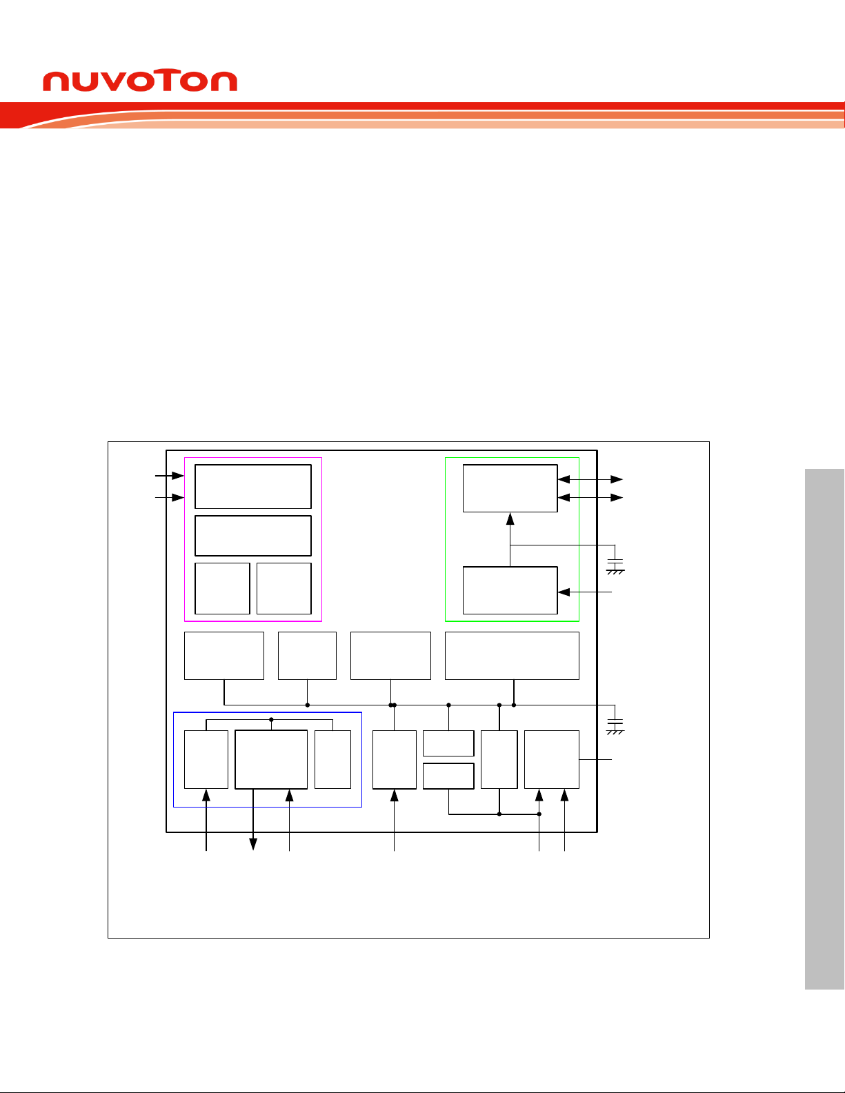
In this chip, the power distribution is divided into three segments.
Analog power from AVDD and AVSS provides the power for analog components
operation.
Digital power from VDD and VSS supplies the power to the internal regulator which
provides a fixed 1.8 V power for digital operation and I/O pins.
USB transceiver power from V
Battery power from V
The outputs of internal voltage regulators, LDO and V
should be located close to the corresponding pin. Analog power (AVDD) should be the same
voltage level with the digital power (VDD). Figure 6.2-1 shows the NuMicro
NUC029LEE/NUC029SEE power distribution.
offers the power for operating the USB transceiver.
BUS
supplies the RTC and external 32.768 kHz crystal.
BAT
, require an external capacitor which
DD33
®
Aug, 2018 Page 31 of 497 Rev 1.00
Figure 6.2-1 NuMicro® NUC029LEE/NUC029SEE Power Distribution Diagram
Page 32
NuMicro® NUC029LEE/NUC029SEE
NUMICRO
®
NUC029LEE/NUC029SEE TECHNICAL REFERENCE MANUAL
Address Space
Token
Controllers
Flash and SRAM Memory Space
0x0000_0000 – 0x0001_FFFF
FLASH_BA
FLASH Memory Space (128 KB)
0x2000_0000 – 0x2000_3FFF
SRAM_BA
SRAM Memory Space (16 KB)
AHB Controllers Space (0x5000_0000 – 0x501F_FFFF)
0x5000_0000 – 0x5000_01FF
GCR_BA
System Global Control Registers
0x5000_0200 – 0x5000_02FF
CLK_BA
Clock Control Registers
0x5000_0300 – 0x5000_03FF
INT_BA
Interrupt Multiplexer Control Registers
0x5000_4000 – 0x5000_7FFF
GPIO_BA
GPIO Control Registers
0x5000_8000 – 0x5000_BFFF
PDMA_BA
Peripheral DMA Control Registers
0x5000_C000 – 0x5000_FFFF
FMC_BA
Flash Memory Control Registers
0x5001_0000 – 0x5001_03FF
EBI_BA
External Bus Interface Control Registers
APB1 Controllers Space (0x4000_0000 ~ 0x400F_FFFF)
0x4000_4000 – 0x4000_7FFF
WDT_BA
Watchdog Timer Control Registers
0x4000_8000 – 0x4000_BFFF
RTC_BA
Real Time Clock (RTC) Control Register
0x4001_0000 – 0x4001_3FFF
TMR01_BA
Timer0/Timer1 Control Registers
0x4002_0000 – 0x4002_3FFF
I2C0_BA
I2C0 Interface Control Registers
0x4003_0000 – 0x4003_3FFF
SPI0_BA
SPI0 with master/slave function Control Registers
0x4003_4000 – 0x4003_7FFF
SPI1_BA
SPI1 with master/slave function Control Registers
0x4004_0000 – 0x4004_3FFF
PWMA_BA
PWM0/1/2/3 Control Registers
0x4005_0000 – 0x4005_3FFF
UART0_BA
UART0 Control Registers
0x4006_0000 – 0x4006_3FFF
USBD_BA
USB 2.0 FS device Controller Registers
0x400E_0000 – 0x400E_FFFF
ADC_BA
Analog-Digital-Converter (ADC) Control Registers
APB2 Controllers Space (0x4010_0000 ~ 0x401F_FFFF)
0x4011_0000 – 0x4011_3FFF
TMR23_BA
Timer2/Timer3 Control Registers
0x4012_0000 – 0x4012_3FFF
I2C1_BA
I2C1 Interface Control Registers
0x4014_0000 – 0x4014_3FFF
PWMB_BA
PWM4/5 Control Registers
0x4015_0000 – 0x4015_3FFF
UART1_BA
UART1 Control Registers
0x4015_4000 – 0x4015_7FFF
UART2_BA
UART2 Control Registers
32-bit Arm® Cortex®-M0 Microcontroller
6.2.4 System Memory Map
The NuMicro® NUC029LEE/NUC029SEE provides 4G-byte addressing space. The memory locations
assigned to each on-chip controllers are shown in the following table. The detailed register definition,
memory space, and programming detailed will be described in the following sections for each on-chip
peripheral. The NuMicro® NUC029LEE/NUC029SEE only supports little-endian data format.
Aug, 2018 Page 32 of 497 Rev 1.00
Page 33
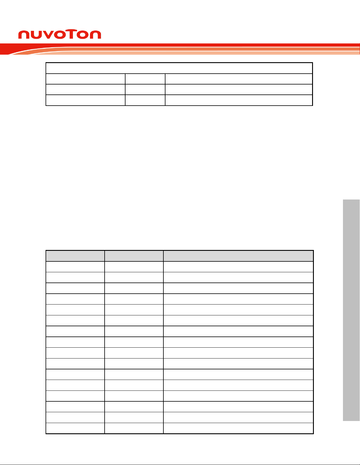
NuMicro® NUC029LEE/NUC029SEE
NUMICRO
®
NUC029LEE/NUC029SEE TECHNICAL REFERENCE MANUAL
System Controllers Space (0xE000_E000 ~ 0xE000_EFFF)
0xE000_E010 – 0xE000_E0FF
SCS_BA
System Timer Control Registers
0xE000_E100 – 0xE000_ECFF
SCS_BA
External Interrupt Controller Control Registers
0xE000_ED00 – 0xE000_ED8F
SCS_BA
System Control Registers
Register
Bit
Description
IPRSTC1
[3] EBI_RST
EBI Controller Reset (Write-protection Bit)
IPRSTC1
[2] PDMA_RST
PDMA Controller Reset (Write Protect)
IPRSTC1
[1] CPU_RST
CPU Kernel One-Shot Reset (Write Protect)
IPRSTC1
[0] CHIP_RST
CHIP One-Shot Reset (Write Protect)
BODCR
[7] LVR_EN
Low Voltage Reset Enable Bit (Write Protect)
BODCR
[5] BOD_LPM
Brown-Out Detector Low Power Mode (Write Protect)
BODCR
[3] BOD_RSTEN
Brown-Out Reset Enable Bit (Write Protect)
BODCR
[2:1] BOD_VL
Brown-Out Detector Threshold Voltage Selection (Write Protect)
BODCR
[0] BOD_EN
Brown-Out Detector Enable Bit (Write Protect)
PORCR
[15:0] POR_DIS_CODE
Power-On-Reset Enable Bit (Write Protect)
REGWRPROT
[7:0] REGWRPROT
Register Write-Protection Code (Write Only)
REGWRPROT
[0] REGPROTDIS
Register Write-Protection Disable Index (Read Only)
NMI_SEL
[8] NMI_EN
NMI Interrupt Enable Bit (Write Protect)
PWRCON
[8] PD_WAIT_CPU
Power-Down Entry Condition Control (Write Protect)
PWRCON
[7] PWR_DOWN_EN
System Power-Down Enable Bit (Write Protect)
PWRCON
[5] PD_WU_INT_EN
Power-Down Mode Wake-Up Interrupt Enable Bit (Write Protect)
32-bit Arm® Cortex®-M0 Microcontroller
Table 6.2-1 Address Space Assignments for On-Chip Controllers
6.2.5 Register Lock
Some of the system control registers need to be protected to avoid inadvertent write and disturb the
chip operation. These system control registers are protected after the power on reset till user to
disable register protection. For user to program these protected registers, a register protection disable
sequence needs to be followed by a special programming. The register protection disable sequence is
writing the data “59h”, “16h” “88h” to the register REGWRPROT address at 0x5000_0100
continuously. Any different data value, different sequence or any other write to other address during
these three data writing will abort the whole sequence.
After the protection is disabled, user can check the protection disable bit at address 0x5000_0100 bit0,
1 is protection disable, and 0 is protection enable. Then user can update the target protected register
value and then write any data to the address “0x5000_0100” to enable register protection.
The protected registers are listed as following table.
Aug, 2018 Page 33 of 497 Rev 1.00
Page 34
NuMicro® NUC029LEE/NUC029SEE
NUMICRO
®
NUC029LEE/NUC029SEE TECHNICAL REFERENCE MANUAL
PWRCON
[4] PD_WU_DLY
Wake-Up Delay Counter Enable Bit (Write Protect)
PWRCON
[3] OSC10K_EN
10 KHz Internal Low Speed RC Oscillator (LIRC) Enable Bit (Write
Protect)
PWRCON
[2] OSC22M_EN
22.1184 MHz Internal High Speed RC Oscillator (HIRC) Enable Bit
(Write Protect)
PWRCON
[1] XTL32K_EN
32.768 KHz External Low Speed Crystal Oscillator (LXT) Enable Bit
(Write Protect)
PWRCON
[0] XTL12M_EN
4~24 MHz External High Speed Crystal Oscillator (HXT) Enable Bit
(Write Protect)
APBCLK
[0] WDT_EN
Watchdog Timer Clock Enable Bit (Write Protect)
CLKSEL0
[5:3] STCLK_S
Cortex®-M0 SysTick Clock Source Select (Write Protect)
CLKSEL0
[2:0] HCLK_S
HCLK Clock Source Select (Write Protect)
CLKSEL1
[1:0] WDT_S
Watchdog Timer Clock Source Select (Write Protect)
ISPCON
[6] ISPFF
ISP Fail Flag (Write Protect)
ISPCON
[5] LDUEN
LDROM Update Enable Bit (Write Protect)
ISPCON
[4] CFGUEN
Enable Config Update By ISP (Write Protect)
ISPCON
[3] APUEN
APROM Update Enable Bit (Write Protect)
ISPCON
[1] BS
Boot Select (Write Protect )
ISPCON
[0] ISPEN
ISP Enable Bit (Write Protect )
ISPTRG
[0] ISPGO
ISP Start Trigger (Write-Protection Bit)
FATCON
[4] FOMSEL0
Chip Frequency Optimization Mode Select 0 (Write-Protection Bit)
ISPSTA
[6] ISPFF
ISP Fail Flag (Write-Protection Bit)
TCSR0
[31] DBGACK_TMR
ICE Debug Mode Acknowledge Disable Bit (Write Protect)
TCSR1
[31] DBGACK_TMR
ICE Debug Mode Acknowledge Disable Bit (Write Protect)
TCSR2
[31] DBGACK_TMR
ICE Debug Mode Acknowledge Disable Bit (Write Protect)
TCSR3
[31] DBGACK_TMR
ICE Debug Mode Acknowledge Disable Bit (Write Protect)
WTCR
[31] DBGACK_WDT
ICE Debug Mode Acknowledge Disable Bit (Write Protect)
WTCR
[10:8] WTIS
Watchdog Timer Time-Out Interval Selection (Write Protect)
WTCR
[7] WTE
Watchdog Timer Enable Bit (Write Protect)
WTCR
[6] WTIE
Watchdog Timer Time-Out Interrupt Enable Bit (Write Protect)
WTCR
[4] WTWKE
Watchdog Timer Time-Out Wake-Up Function Control (Write Protect)
WTCR
[1] WTRE
Watchdog Timer Reset Enable Bit (Write Protect)
WTCRALT
[1:0] WTRDSEL
Watchdog Timer Reset Delay Selection (Write Protect)
32-bit Arm® Cortex®-M0 Microcontroller
6.2.6 Auto Trim
This chip supports auto-trim function: the HIRC trim (48 MHz and 22.1184 MHz RC oscillator),
Aug, 2018 Page 34 of 497 Rev 1.00
Page 35

NuMicro® NUC029LEE/NUC029SEE
NUMICRO
®
NUC029LEE/NUC029SEE TECHNICAL REFERENCE MANUAL
32-bit Arm® Cortex®-M0 Microcontroller
according to the accurate LXT (32.768 kHz crystal oscillator) or internal USB synchronous mode,
automatically gets accurate HIRC output frequency, 0.25 % deviation within all temperature ranges.
For instance, the system needs an accurate 22.1184 MHz clock. In such case, if users do not want to
use PLL as the system clock source, they need to solder 32.768 kHz crystal in system, and set
FREQSEL (SYS_IRCTCTL[1:0] trim frequency selection) to “01”, and the auto-trim function will be
enabled. Interrupt status bit FREQ_LOCK (SYS_IRCTSTS[0] HIRC frequency lock status) “1”
indicates the HIRC output frequency is accurate within 0.25% deviation. To get better results, it is
recommended to set both TRIM_LOOP (SYS_IRCTCTL[5:4]) Trim Calculation Loop and
TRIM_RETRY_CNT (SYS_IRCTCTL[7:6] Trim Value Update Limitation Count) to “11”.
Another example is that the system needs an accurate 48 MHz clock for USB application. In such
case, if neither using use PLL as the system clock source, user has to set FREQSEL
(SYS_HIRCTCTL1[1:0] trim frequency selection) to “01”, and the auto-trim function will be enabled.
Status bit FREQLOCK (SYS_HIRCTISTS[8] HIRC Frequency Lock Status) “1” indicates the HIRC48
output frequency is accurate within 0.25% deviation.
Aug, 2018 Page 35 of 497 Rev 1.00
Page 36
NUMICRO
®
NUC029LEE/NUC029SEE TECHNICAL REFERENCE MANUAL
6.2.7 Register Map
Register
Offset
R/W
Description
Reset Value
GCR Base Address:
GCR_BA = 0x5000_0000
PDID
GCR_BA+0x00
R
Part Device Identification Number Register
0x2014_0018
[1]
RSTSRC
GCR_BA+0x04
R/W
System Reset Source Register
0x0000_00XX
IPRSTC1
GCR_BA+0x08
R/W
Peripheral Reset Control Register 1
0x0000_0000
IPRSTC2
GCR_BA+0x0C
R/W
Peripheral Reset Control Register 2
0x0000_0000
BODCR
GCR_BA+0x18
R/W
Brown-out Detector Control Register
0x0000_008X
TEMPCR
GCR_BA+0x1C
R/W
Temperature Sensor Control Register
0x0000_0000
PORCR
GCR_BA+0x24
R/W
Power-on-reset Controller Register
0x0000_XXXX
GPA_MFP
GCR_BA+0x30
R/W
GPIOA Multiple Function and Input Type Control Register
0x0000_0000
GPB_MFP
GCR_BA+0x34
R/W
GPIOB Multiple Function and Input Type Control Register
0x0000_0000
GPC_MFP
GCR_BA+0x38
R/W
GPIOC Multiple Function and Input Type Control Register
0x0000_0000
GPE_MFP
GCR_BA+0x40
R/W
GPIOE Multiple Function and Input Type Control Register
0x0000_0000
GPF_MFP
GCR_BA+0x44
R/W
GPIOF Multiple Function and Input Type Control Register
0x0000_000X
ALT_MFP
GCR_BA+0x50
R/W
Alternative Multiple Function Pin Control Register
0x0000_0000
ALT_MFP2
GCR_BA+0x5C
R/W
Alternative Multiple Function Pin Control Register 2
0x0000_0000
IRCTCTL
GCR_BA+0x80
R/W
IRC Trim Control Register
0x0000_0000
IRCTIEN
GCR_BA+0x84
R/W
IRC Trim Interrupt Enable Register
0x0000_0000
IRCTSTS
GCR_BA+0x88
R/W
IRC Trim Interrupt Status Register
0x0000_0000
HIRCTCTL
GCR_BA+0x90
R/W
HIRC Trim Control Register
0x0008_0000
HIRCTIEN
GCR_BA+0x94
R/W
HIRC Trim Interrupt Enable Register
0x0000_0000
HIRCTSTS
GCR_BA+0x98
R/W
HIRC Trim Interrupt Status Register
0x0000_0000
REGWRPROT
GCR_BA+0x100
R/W
Register Write Protection Register
0x0000_0000
R: read only, W: write only, R/W: both read and write
NuMicro® NUC029LEE/NUC029SEE
32-bit Arm® Cortex®-M0 Microcontroller
Note: [1] It depends on the part number.
Aug, 2018 Page 36 of 497 Rev 1.00
Page 37
NuMicro® NUC029LEE/NUC029SEE
NUMICRO
®
NUC029LEE/NUC029SEE TECHNICAL REFERENCE MANUAL
Register
Offset
R/W
Description
Reset Value
PDID
GCR_BA+0x00
R
Part Device Identification Number Register
0x2014_0018
[1]
31
30
29
28
27
26
25
24
PDID
23
22
21
20
19
18
17
16
PDID
15
14
13
12
11
10 9 8
PDID
7 6 5 4 3 2 1
0
PDID
Bits
Description
[31:0]
PDID
Part Device Identification Number
This register reflects device part number code. Software can read this register to identify
which device is used.
32-bit Arm® Cortex®-M0 Microcontroller
6.2.8 Register Description
Part Device ID Code Register (PDID)
[1] Each part number has a unique default reset value.
Aug, 2018 Page 37 of 497 Rev 1.00
Page 38
NuMicro® NUC029LEE/NUC029SEE
NUMICRO
®
NUC029LEE/NUC029SEE TECHNICAL REFERENCE MANUAL
Register
Offset
R/W
Description
Reset Value
RSTSRC
GCR_BA+0x04
R/W
System Reset Source Register
0x0000_00XX
31
30
29
28
27
26
25
24
Reserved
23
22
21
20
19
18
17
16
Reserved
15
14
13
12
11
10 9 8
Reserved
7 6 5 4 3 2 1
0
RSTS_CPU
Reserved
RSTS_SYS
RSTS_BOD
RSTS_LVR
RSTS_WDT
RSTS_RESET
RSTS_POR
Bits
Description
[31:8]
Reserved
Reserved.
[7]
RSTS_CPU
CPU Reset Flag
The RSTS_CPU flag Is set by hardware if software writes CPU_RST (IPRSTC1[1]) 1 To
reset Cortex®-M0 kernel and flash memory controller (FMC).
0 = No reset from CPU.
1 = Cortex®-M0 CPU kernel and FMC are reset by software setting
CPU_RST(IPRSTC1[1]) to 1.
Note: Write 1 to clear this bit to 0.
[6]
Reserved
Reserved.
[5]
RSTS_SYS
SYS Reset Flag
The RSTS_SYS flag Is set by the “Reset Signal” from the Cortex®-M0 kernel to indicate
the previous reset source.
0 = No reset from Cortex®-M0.
1 = The Cortex®-M0 had issued the reset signal to reset the system by writing 1 to bit
SYSRESETREQ (AIRCR[2], Application Interrupt and Reset Control Register, address =
0xE000ED0C) in system control registers of Cortex®-M0 kernel.
Note: Write 1 to clear this bit to 0.
[4]
RSTS_BOD
Brown-Out Detector Reset Flag
The RSTS_BOD flag is set by the “Reset Signal” from the Brown-Out Detector to indicate
the previous reset source.
0 = No reset from BOD.
1 = The BOD had issued the reset signal to reset the system.
Note: Write 1 to clear this bit to 0.
[3]
RSTS_LVR
Low Voltage Reset Flag
The RSTS_LVR flag is set by the “Reset Signal” from the Low-Voltage-Reset controller to
32-bit Arm® Cortex®-M0 Microcontroller
System Reset Source Register (RSTSRC)
This register provides specific information for software to identify this chip’s reset source from last
operation.
Aug, 2018 Page 38 of 497 Rev 1.00
Page 39

NuMicro® NUC029LEE/NUC029SEE
NUMICRO
®
NUC029LEE/NUC029SEE TECHNICAL REFERENCE MANUAL
indicate the previous reset source.
0 = No reset from LVR.
1 = The LVR controller had issued the reset signal to reset the system.
Note: Write 1 to clear this bit to 0.
[2]
RSTS_WDT
Watchdog Timer Reset Flag
The RSTS_WDT flag is set by the “Reset Signal” from the watchdog timer or window
watchdog timer to indicate the previous reset source.
0 = No reset from watchdog timer or window watchdog timer.
1 = The watchdog timer or window watchdog timer had issued the reset signal to reset the
system.
Note1: Write 1 to clear this bit to 0.
Note2: Watchdog Timer register WTRF(WTCR[2]) bit is set if the system has been reset
by WDT time-out reset. Window Watchdog Timer register WWDTRF(WWDTSR) bit is set
if the system has been reset by WWDT time-out reset.
[1]
RSTS_RESET
Reset Pin Reset Flag
The RSTS_RESET flag is set by the “Reset Signal” from the nRESET Pin to indicate the
previous reset source
0 = No reset from nRESET pin.
1 = The Pin nRESET had issued the reset signal to reset the system.
Note: Write 1 to clear this bit to 0.
[0]
RSTS_POR
Power-On Reset Flag
The RSTS_POR Flag is set by the “Reset Signal” from the Power-On Reset (POR)
vontroller or bit CHIP_RST (IPRSTC1[0]) to indicate the previous reset source
0 = No reset from POR or CHIP_RST (IPRSTC1[0]).
1 = Power-on Reset (POR) or CHIP_RST (IPRSTC1[0]) had issued the reset signal to
reset the system.
Note: Write 1 to clear this bit to 0.
32-bit Arm® Cortex®-M0 Microcontroller
Aug, 2018 Page 39 of 497 Rev 1.00
Page 40
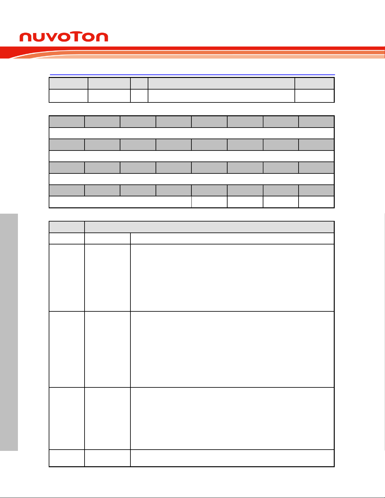
NuMicro® NUC029LEE/NUC029SEE
NUMICRO
®
NUC029LEE/NUC029SEE TECHNICAL REFERENCE MANUAL
Register
Offset
R/W
Description
Reset Value
IPRSTC1
GCR_BA+0x08
R/W
Peripheral Reset Control Register 1
0x0000_0000
31
30
29
28
27
26
25
24
Reserved
23
22
21
20
19
18
17
16
Reserved
15
14
13
12
11
10 9 8
Reserved
7 6 5 4 3 2 1
0
Reserved
EBI_RST
PDMA_RST
CPU_RST
CHIP_RST
Bits
Description
[31:4]
Reserved
Reserved.
[3]
EBI_RST
EBI Controller Reset (Write-protection Bit)
Set this bit to 1 will generate a reset signal to the EBI. User need to set this bit to 0 to
release from the reset state.
This bit is the protected bit, It means programming this bit needs to write “59h”, “16h”,
“88h” to address 0x5000_0100 to disable register protection. Refer to the register
REGWRPROT at address GCR_BA+0x100
1 = EBI controller reset
0 = EBI controller normal operation
[2]
PDMA_RST
PDMA Controller Reset (Write Protect)
Setting this bit to 1 will generate a reset signal to the PDMA. User needs to set this bit to 0
to release from reset state.
0 = PDMA controller normal operation.
1 = PDMA controller reset.
Note1: This bit is the protected bit, and programming it needs to write “59h”, “16h”, and
“88h” to address 0x5000_0100 to disable register protection. Refer to the register
REGWRPROT at address GCR_BA+0x100.
Note2: Setting PDMA_RST bit to 1 will generate asynchronous reset signal to PDMA
module. Users need to set PDMA_RST to 0 to release PDMA module from reset state.
[1]
CPU_RST
CPU Kernel One-Shot Reset (Write Protect)
Setting this bit will only reset the CPU kernel and Flash Memory Controller(FMC), and this
bit will automatically return 0 after the two clock cycles
0 = CPU normal operation.
1 = CPU one-shot reset.
Note: This bit is the protected bit, and programming it needs to write “59h”, “16h”, and
“88h” to address 0x5000_0100 to disable register protection. Refer to the register
REGWRPROT at address GCR_BA+0x100.
[0]
CHIP_RST
CHIP One-Shot Reset (Write Protect)
Setting this bit will reset the whole chip, including CPU kernel and all peripherals, and this
32-bit Arm® Cortex®-M0 Microcontroller
Peripheral Reset Control Register 1 (IPRSTC1) .
Aug, 2018 Page 40 of 497 Rev 1.00
Page 41
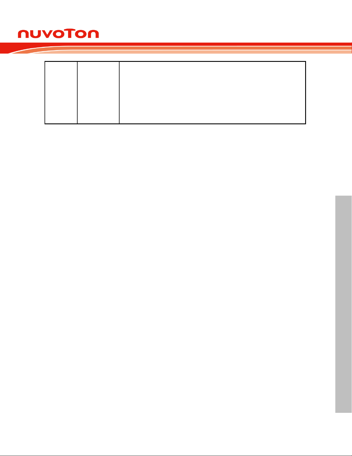
NuMicro® NUC029LEE/NUC029SEE
NUMICRO
®
NUC029LEE/NUC029SEE TECHNICAL REFERENCE MANUAL
bit will automatically return to 0 after the 2 clock cycles.
The CHIP_RST is the same as the POR reset, all the chip controllers are reset and the
chip setting from flash are also reload.
For the difference between CHIP_RST and SYSRESETREQ, please refer to section 5.2.2
0 = CHIP normal operation.
1 = CHIP one-shot reset.
Note: This bit is the protected bit, and programming it needs to write “59h”, “16h”, and
“88h” to address 0x5000_0100 to disable register protection. Refer to the register
REGWRPROT at address GCR_BA+0x100.
32-bit Arm® Cortex®-M0 Microcontroller
Aug, 2018 Page 41 of 497 Rev 1.00
Page 42
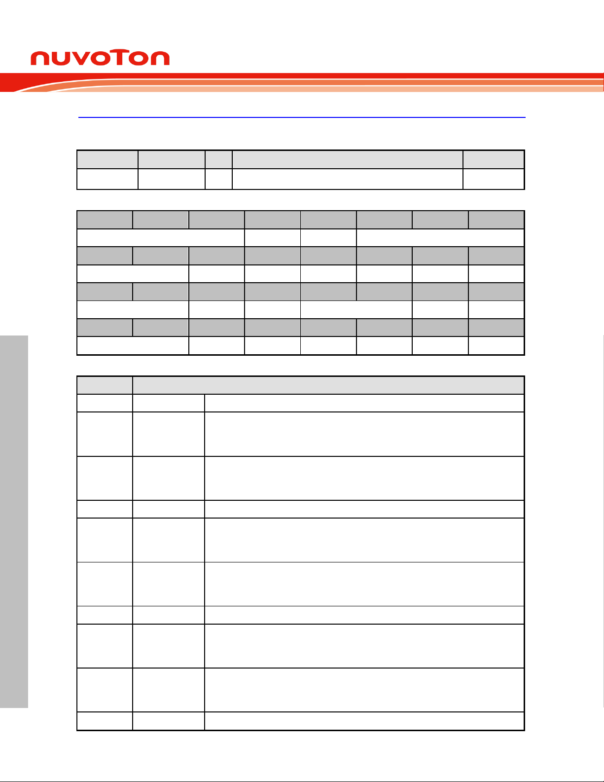
NuMicro® NUC029LEE/NUC029SEE
NUMICRO
®
NUC029LEE/NUC029SEE TECHNICAL REFERENCE MANUAL
Register
Offset
R/W
Description
Reset Value
IPRSTC2
GCR_BA+0x0C
R/W
Peripheral Reset Control Register 2
0x0000_0000
31
30
29
28
27
26
25
24
Reserved
ADC_RST
USBD_RST
Reserved
23
22
21
20
19
18
17
16
Reserved
PWM45_RST
PWM03_RST
Reserved
UART2_RST
UART1_RST
UART0_RST
15
14
13
12
11
10 9 8
Reserved
SPI1_RST
SPI0_RST
Reserved
I2C1_RST
I2C0_RST
7 6 5 4 3 2 1
0
Reserved
TMR3_RST
TMR2_RST
TMR1_RST
TMR0_RST
GPIO_RST
Reserved
Bits
Description
[31:39]
Reserved
Reserved.
[28]
ADC_RST
ADC Controller Reset
0 = ADC controller normal operation.
1 = ADC controller reset.
[27]
USBD_RST
USB Device Controller Reset
0 = USB device controller normal operation.
1 = USB device controller reset.
[26:22]
Reserved
Reserved.
[21]
PWM45_RST
PWM45 Controller Reset
0 = PWM45 controller normal operation.
1 = PWM45 controller reset.
[20]
PWM03_RST
PWM03 Controller Reset
0 = PWM03 controller normal operation.
1 = PWM03 controller reset.
[19]
Reserved
Reserved.
[18]
UART2_RST
UART2 Controller Reset
0 = UART2 controller normal operation.
1 = UART2 controller reset.
[17]
UART1_RST
UART1 Controller Reset
0 = UART1 controller normal operation.
1 = UART1 controller reset.
[16]
UART0_RST
UART0 Controller Reset
32-bit Arm® Cortex®-M0 Microcontroller
Peripheral Reset Control Register 2 (IPRSTC2)
Setting these bits to 1 will generate asynchronous reset signals to the corresponding module. User
needs to set these bits to 0 to release the corresponding module from reset state.
Aug, 2018 Page 42 of 497 Rev 1.00
Page 43
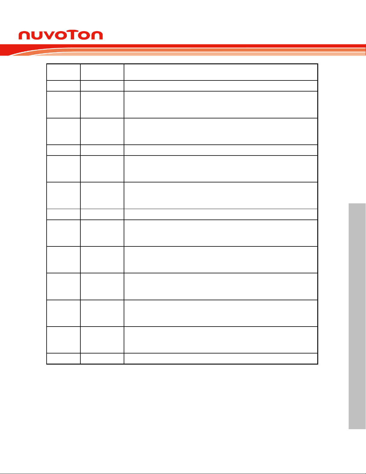
NuMicro® NUC029LEE/NUC029SEE
NUMICRO
®
NUC029LEE/NUC029SEE TECHNICAL REFERENCE MANUAL
0 = UART0 controller normal operation.
1 = UART0 controller reset.
[15:14]
Reserved
Reserved.
[13]
SPI1_ RST
SPI1 Controller Reset
0 = SPI1 controller normal operation.
1 = SPI1 controller reset.
[12]
SPI0_ RST
SPI0 Controller Reset
0 = SPI0 controller normal operation.
1 = SPI0 controller reset.
[11:10]
Reserved
Reserved.
[9]
I2C1_RST
I2C1 Controller Reset
0 = I2C1 controller normal operation.
1 = I2C1 controller reset.
[8]
I2C0_RST
I2C0 Controller Reset
0 = I2C0 controller normal operation.
1 = I2C0 controller reset.
[7:6]
Reserved
Reserved.
[5]
TMR3_RST
Timer3 Controller Reset
0 = Timer3 controller normal operation.
1 = Timer3 controller reset.
[4]
TMR2_RST
Timer2 Controller Reset
0 = Timer2 controller normal operation.
1 = Timer2 controller reset.
[3]
TMR1_RST
Timer1 Controller Reset
0 = Timer1 controller normal operation.
1 = Timer1 controller reset.
[2]
TMR0_RST
Timer0 Controller Reset
0 = Timer0 controller normal operation.
1 = Timer0 controller reset.
[1]
GPIO_RST
GPIO Controller Reset
0 = GPIO controller normal operation.
1 = GPIO controller reset.
[0]
Reserved
Reserved.
32-bit Arm® Cortex®-M0 Microcontroller
Aug, 2018 Page 43 of 497 Rev 1.00
Page 44
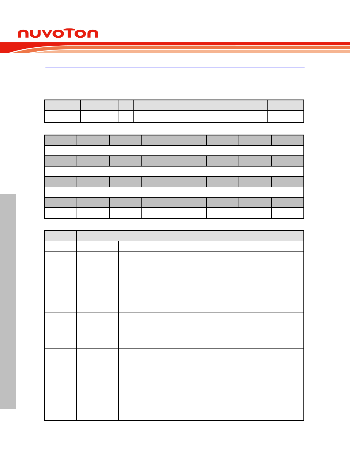
NuMicro® NUC029LEE/NUC029SEE
NUMICRO
®
NUC029LEE/NUC029SEE TECHNICAL REFERENCE MANUAL
Register
Offset
R/W
Description
Reset Value
BODCR
GCR_BA+0x18
R/W
Brown-out Detector Control Register
0x0000_008X
31
30
29
28
27
26
25
24
Reserved
23
22
21
20
19
18
17
16
Reserved
15
14
13
12
11
10 9 8
Reserved
7 6 5 4 3 2 1
0
LVR_EN
BOD_OUT
BOD_LPM
BOD_INTF
BOD_RSTEN
BOD_VL
BOD_EN
Bits
Description
[31:8]
Reserved
Reserved.
[7]
LVR_EN
Low Voltage Reset Enable Bit (Write Protect)
The LVR function reset the chip when the input power voltage is lower than LVR circuit
setting. LVR function is enabled by default.
0 = Low Voltage Reset function Disabled.
1 = Low Voltage Reset function Enabled – After enabling the bit, the LVR function will be
active with 100us delay for LVR output stable (default).
Note: This bit is the protected bit, and programming it needs to write “59h”, “16h”, and
“88h” to address 0x5000_0100 to disable register protection. Refer to the register
REGWRPROT at address GCR_BA+0x100.
[6]
BOD_OUT
Brown-Out Detector Output Status
0 = Brown-out Detector output status is 0. It means the detected voltage is higher than
BOD_VL setting or BOD_EN is 0.
1 = Brown-out Detector output status is 1. It means the detected voltage is lower than
BOD_VL setting. If the BOD_EN is 0, BOD function disabled, this bit always responds to 0.
[5]
BOD_LPM
Brown-Out Detector Low Power Mode (Write Protect)
0 = BOD operated in Normal mode (default).
1 = BOD Low Power mode Enabled.
Note1: The BOD consumes about 100 uA in Normal mode, and the low power mode can
reduce the current to about 1/10 but slow the BOD response.
Note2: This bit is the protected bit, and programming it needs to write “59h”, “16h”, and
“88h” to address 0x5000_0100 to disable register protection. Refer to the register
REGWRPROT at address GCR_BA+0x100.
[4]
BOD_INTF
Brown-Out Detector Interrupt Flag
0 = Brown-out Detector does not detect any voltage draft at VDD down through or up
32-bit Arm® Cortex®-M0 Microcontroller
Brown-out Detector Control Register (BODCR)
Partial of the BODCR control registers values are initiated by the flash configuration and partial bits
are write-protected bit. Programming write-protected bits needs to write “59h”, “16h”, “88h” to address
0x5000_0100 to disable register protection. Refer to the register REGWRPROT at address
GCR_BA+0x100.
Aug, 2018 Page 44 of 497 Rev 1.00
Page 45

NuMicro® NUC029LEE/NUC029SEE
NUMICRO
®
NUC029LEE/NUC029SEE TECHNICAL REFERENCE MANUAL
through the voltage of BOD_VL setting.
1 = When Brown-out Detector detects the VDD is dropped down through the voltage of
BOD_VL setting or the VDD is raised up through the voltage of BOD_VL setting, this bit is
set to 1 and the Brown-out interrupt is requested if Brown-out interrupt is enabled.
Note: Write 1 to clear this bit to 0.
[3]
BOD_RSTEN
Brown-Out Reset Enable Bit (Write Protect)
0 = Brown-out “INTERRUPT” function Enabled.
1 = Brown-out “RESET” function Enabled.
While the Brown-out Detector function is enabled (BOD_EN high) and BOD reset function
is enabled (BOD_RSTEN high), BOD will assert a signal to reset chip when the detected
voltage is lower than the threshold (BOD_OUT high).
Note1: While the BOD function is enabled (BOD_EN high) and BOD interrupt function is
enabled (BOD_RSTEN low), BOD will assert an interrupt if BOD_OUT is high. BOD
interrupt will keep till to the BOD_EN set to 0. BOD interrupt can be blocked by disabling
the NVIC BOD interrupt or disabling BOD function (set BOD_EN low).
Note2: The default value is set by flash controller user configuration register
CBORST(CONFIG0[20]) bit.
Note3: This bit is the protected bit. It means programming this needs to write “59h”, “16h”,
“88h” to address 0x5000_0100 to disable register protection. Refer to the register
REGWRPROT at address GCR_BA+0x100.
[2:1]
BOD_VL
Brown-Out Detector Threshold Voltage Selection (Write Protect)
The default value is set by flash momory controller user configuration register
CBOV(CONFIG0[22:21]) bit .
00 = Brown-out voltage is 2.2V.
01 = Brown-out voltage is 2.7V.
10 = Brown-out voltage is 3.7V.
11 = Brown-out voltage is 4.4V.
Note: This bit is the protected bit. It means programming this needs to write “59h”, “16h”,
“88h” to address 0x5000_0100 to disable register protection. Refer to the register
REGWRPROT at address GCR_BA+0x100.
[0]
BOD_EN
Brown-Out Detector Enable Bit (Write Protect)
The default value is set by flash memory controller user configuration register
CBODEN(CONFIG0[23]) bit.
0 = Brown-out Detector function Disabled.
1 = Brown-out Detector function Enabled.
Note: This bit is the protected bit. It means programming this needs to write “59h”, “16h”,
“88h” to address 0x5000_0100 to disable register protection. Refer to the register
REGWRPROT at address GCR_BA+0x100.
32-bit Arm® Cortex®-M0 Microcontroller
Aug, 2018 Page 45 of 497 Rev 1.00
Page 46
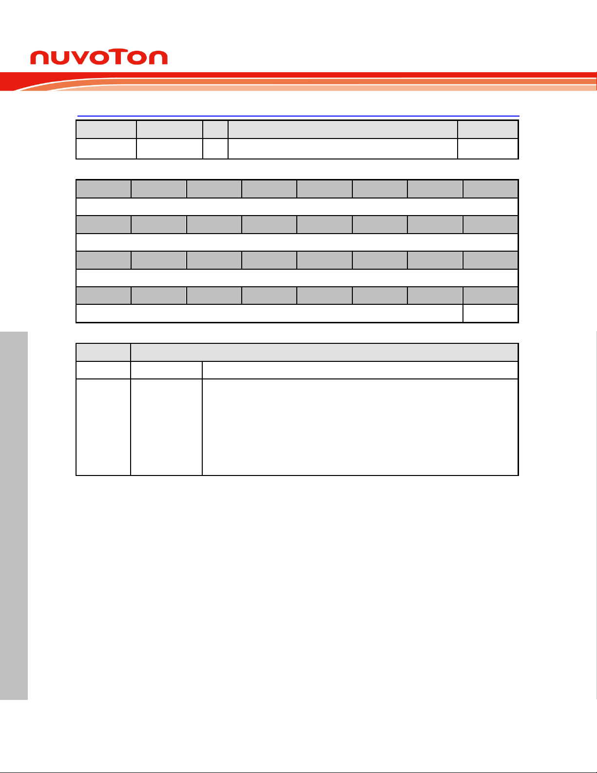
NuMicro® NUC029LEE/NUC029SEE
NUMICRO
®
NUC029LEE/NUC029SEE TECHNICAL REFERENCE MANUAL
Register
Offset
R/W
Description
Reset Value
TEMPCR
GCR_BA+0x1C
R/W
Temperature Sensor Control Register
0x0000_0000
31
30
29
28
27
26
25
24
Reserved
23
22
21
20
19
18
17
16
Reserved
15
14
13
12
11
10 9 8
Reserved
7 6 5 4 3 2 1
0
Reserved
VTEMP_EN
Bits
Description
[31:1]
Reserved
Reserved.
[0]
VTEMP_EN
Temperature Sensor Enable Bit
This bit is used to enable/disable temperature sensor function.
0 = Temperature sensor function Disabled (default).
1 = Temperature sensor function Enabled.
Note: After this bit is set to 1, the value of temperature can be obtained from ADC
conversion result by ADC channel selecting channel 7 and alternative multiplexer channel
selecting temperature sensor. Please refer to the ADC function chapter for detail ADC
conversion functional description.
32-bit Arm® Cortex®-M0 Microcontroller
Temperature Sensor Control Register (TEMPCR)
Aug, 2018 Page 46 of 497 Rev 1.00
Page 47
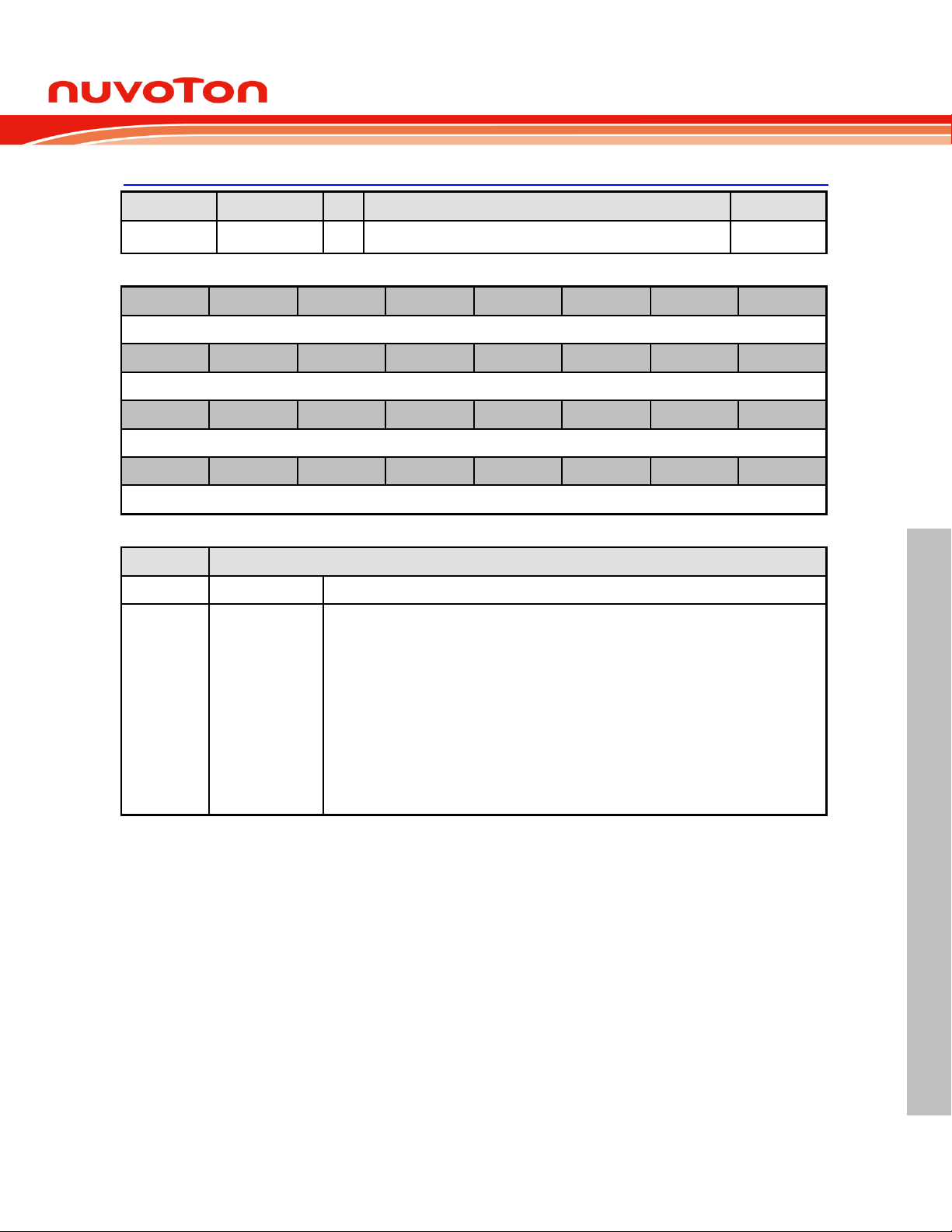
NuMicro® NUC029LEE/NUC029SEE
NUMICRO
®
NUC029LEE/NUC029SEE TECHNICAL REFERENCE MANUAL
Register
Offset
R/W
Description
Reset Value
PORCR
GCR_BA+0x24
R/W
Power-on-reset Controller Register
0x0000_XXXX
31
30
29
28
27
26
25
24
Reserved
23
22
21
20
19
18
17
16
Reserved
15
14
13
12
11
10 9 8
POR_DIS_CODE
7 6 5 4 3 2 1
0
POR_DIS_CODE
Bits
Description
[31:16]
Reserved
Reserved.
[15:0]
POR_DIS_CODE
Power-On-Reset Enable Bit (Write Protect)
When powered on, the POR circuit generates a reset signal to reset the whole chip
function, but noise on the power may cause the POR active again. User can disable
internal POR circuit to avoid unpredictable noise to cause chip reset by writing 0x5AA5 to
this field.
The POR function will be active again when this field is set to another value or chip is
reset by other reset source, including:
nRESET, Watchdog Timer reset, Window Watchdog Timer reset, LVR reset, BOD reset,
ICE reset command and the software-chip reset function
Note: This bit is the protected bit. It means programming this needs to write “59h”, “16h”,
“88h” to address 0x5000_0100 to disable register protection. Refer to the register
REGWRPROT at address GCR_BA+0x100.
32-bit Arm® Cortex®-M0 Microcontroller
Power-on-Reset Control Register (PORCR)
Aug, 2018 Page 47 of 497 Rev 1.00
Page 48
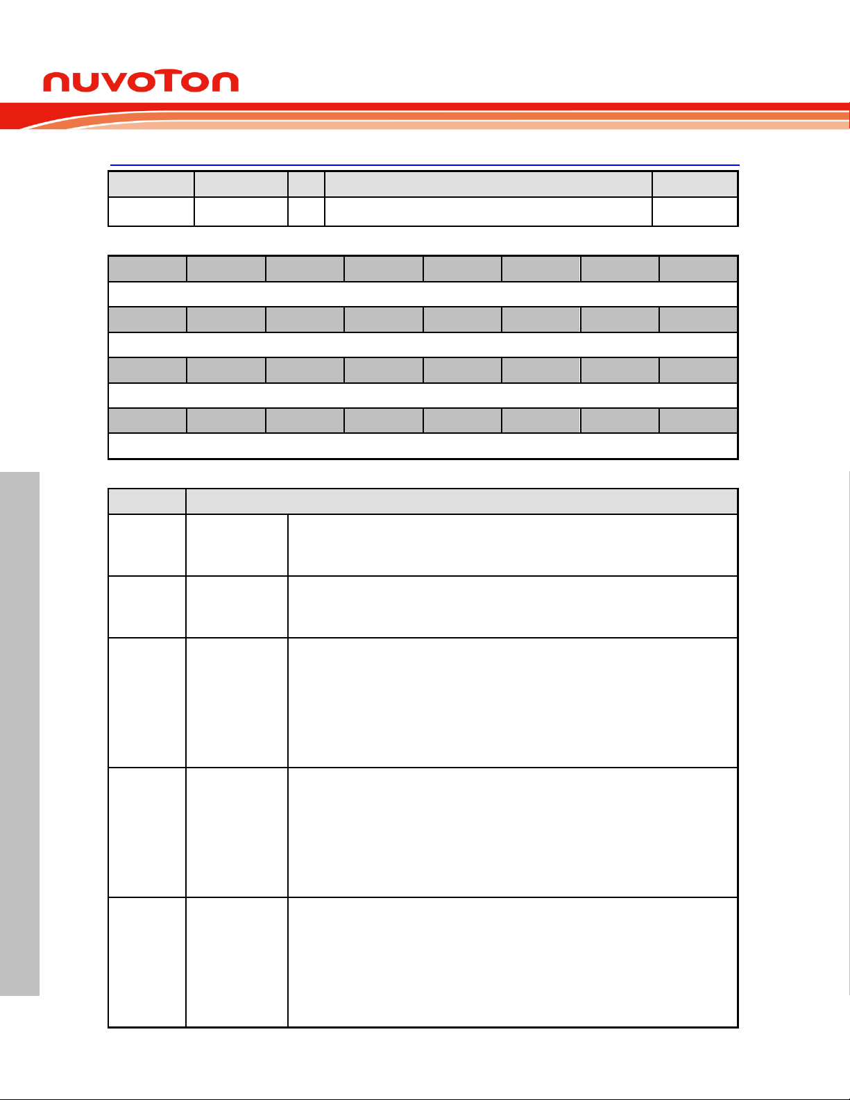
NuMicro® NUC029LEE/NUC029SEE
NUMICRO
®
NUC029LEE/NUC029SEE TECHNICAL REFERENCE MANUAL
Register
Offset
R/W
Description
Reset Value
GPA_MFP
GCR_BA+0x30
R/W
GPIOA Multiple Function and Input Type Control Register
0x0000_0000
31
30
29
28
27
26
25
24
GPA_TYPE
23
22
21
20
19
18
17
16
GPA_TYPE
15
14
13
12
11
10 9 8
GPA_MFP
7 6 5 4 3 2 1
0
GPA_MFP
Bits
Description
[31:16]
GPA_TYPEn
Trigger Function Selection
0 = GPIOA[15:0] I/O input Schmitt Trigger function Disabled.
1 = GPIOA[15:0] I/O input Schmitt Trigger function Enabled.
[15]
GPA_MFP15
PA.15 Pin Function Selection
0 = GPIOA function is selected.
1 = PWM3 function is selected.
[14]
GPA_MFP14
PA.14 Pin Function Selection
Bits EBI_HB_EN[7] (ALT_MFP[23]), EBI_EN (ALT_MFP[11]) and GPA_MFP[14]
determine the PA.14 function.
(EBI_HB_EN, EBI_EN, GPA_MFP14) value and function mapping is as following list.
(0, 0, 0) = GPIO function is selected.
(0, 0, 1) = PWM2 function is selected.
(1, 1, 1) = AD15 function is selected.
[13]
GPA_MFP13
PA.13 Pin Function Selection
Bits EBI_HB_EN[6] (ALT_MFP[22]), EBI_EN (ALT_MFP[11]) and GPA_MFP[13]
determine the PA.13 function.
(EBI_HB_EN, EBI_EN, GPA_MFP13) value and function mapping is as following list.
(0, 0, 0) = GPIO function is selected.
(0, 0, 1) = PWM1 function is selected.
(1, 1, 1) = AD14 function is selected.
[12]
GPA_MFP12
PA.12 Pin Function Selection
Bits EBI_HB_EN[5] (ALT_MFP[21]), EBI_EN (ALT_MFP[11]) and GPA_MFP[12]
determine the PA.12 function.
(EBI_HB_EN, EBI_EN, GPA_MFP12) value and function mapping is as following list.
(0, 0, 0) = GPIO function is selected.
(0, 0, 1) = PWM0 function is selected.
(1, 1, 1) = AD13 function is selected.
32-bit Arm® Cortex®-M0 Microcontroller
GPIOA Multiple Function Pin and Input Type Control Register (GPA_MFP)
Aug, 2018 Page 48 of 497 Rev 1.00
Page 49

NuMicro® NUC029LEE/NUC029SEE
NUMICRO
®
NUC029LEE/NUC029SEE TECHNICAL REFERENCE MANUAL
[11]
GPA_MFP11
PA.11 Pin Function Selection
Bits EBI_EN (ALT_MFP[11]) and GPA_MFP[11] determine the PA.11 function.
(EBI_EN, GPA_MFP11) value and function mapping is as following list.
(0, 0) = GPIO function is selected.
(0, 1) = I2C1_SCL function is selected.
(1, 1) = nRD(EBI) function is selected.
[10]
GPA_MFP10
PA.10 Pin Function Selection
Bits EBI_EN (ALT_MFP[11]) and GPA_MFP[10] determine the PA.10 function.
(EBI_EN, GPA_MFP10) value and function mapping is as following list.
(0, 0) = GPIO function is selected.
(0, 1) = I2C1_SDA function is selected.
(1, 1) = nWR(EBI) function is selected.
[9]
GPA_MFP9
PA.9 Pin Function Selection
Bit GPA_MFP[9] determines the PA.9 function.
0 = GPIO function is selected.
1 = I2C0_SCL function is selected.
[8]
GPA_MFP8
PA.8 Pin Function Selection
Bit GPA_MFP[8] determines the PA.9 function.
0 = GPIO function is selected to the pin PA.8.
1 = I2C0_SDA function is selected to the pin PA.8.
[7]
GPA_MFP7
Reserved.
[6]
GPA_MFP6
PA.6 Pin Function Selection
Bits EBI_EN (ALT_MFP[11]) and GPA_MFP[6] determine the PA.6 function.
(EBI_EN, GPA_MFP6) value and function mapping is as following list.
(0, 0) = GPIO function is selected.
(0, 1) = ADC6 function is selected.
(1, 1) = AD7 function is selected.
[5]
GPA_MFP5
PA.5 Pin Function Selection
Bits EBI_HB_EN[0] (ALT_MFP[16]), EBI_EN (ALT_MFP[11]) and GPA_MFP[5] determine
the PA.5 function.
(EBI_HB_EN, EBI_EN, GPA_MFP5) value and function mapping is as following list,
(0, 0, 0) = GPIO function is selected.
(0, 0, 1) = ADC5 function is selected.
(1, 1, 1) = AD8 function is selected.
[4]
GPA_MFP4
PA.4 Pin Function Selection
Bits EBI_HB_EN[1] (ALT_MFP[17]), EBI_EN (ALT_MFP[11]) and GPA_MFP[4] determine
the PA.4 function.
(EBI_HB_EN, EBI_EN, GPA_MFP4) value and function mapping is as following list.
(0, 0, 0) = GPIO function is selected.
(0, 0, 1) = ADC4 function is selected.
(1, 1, 1) = AD9 function is selected.
32-bit Arm® Cortex®-M0 Microcontroller
Aug, 2018 Page 49 of 497 Rev 1.00
Page 50

NuMicro® NUC029LEE/NUC029SEE
NUMICRO
®
NUC029LEE/NUC029SEE TECHNICAL REFERENCE MANUAL
[3]
GPA_MFP3
PA.3 Pin Function Selection
Bits EBI_HB_EN[2] (ALT_MFP[18]), EBI_EN (ALT_MFP[11]) and GPA_MFP[3] determine
the PA.3 function.
(EBI_HB_EN, EBI_EN, GPA_MFP3) value and function mapping is as following list.
(0, 0, 0) = GPIO function is selected.
(0, 0, 1) = ADC3 function is selected.
(1, 1, 1) = AD10 function is selected.
[2]
GPA_MFP2
PA.2 Pin Function Selection
Bits EBI_HB_EN[3] (ALT_MFP[19]), EBI_EN (ALT_MFP[11]) and GPA_MFP[2] determine
the PA.2 function.
(EBI_HB_EN, EBI_EN, GPA_MFP2) value and function mapping is as following list.
(0, 0, 0) = GPIO function is selected.
(0, 0, 1) = ADC2 function is selected.
(1, 1, 1) = AD11 function is selected.
[1]
GPA_MFP1
PA.1 Pin Function Selection
Bit EBI_HB_EN[4] (ALT_MFP[20]), EBI_EN (ALT_MFP[11]) and GPA_MFP[1] determine
the PA.1 function.
(EBI_HB_EN, EBI_EN, GPA_MFP1) value and function mapping is as following list.
(0, 0, 0) = GPIO function is selected.
(0, 0, 1) = ADC1 function is selected.
(1, 1, 1) = AD12 function is selected.
[0]
GPA_MFP0
PA.0 Pin Function Selection
0 = GPIO function is selected.
1 = ADC0 function is selected.
32-bit Arm® Cortex®-M0 Microcontroller
Aug, 2018 Page 50 of 497 Rev 1.00
Page 51
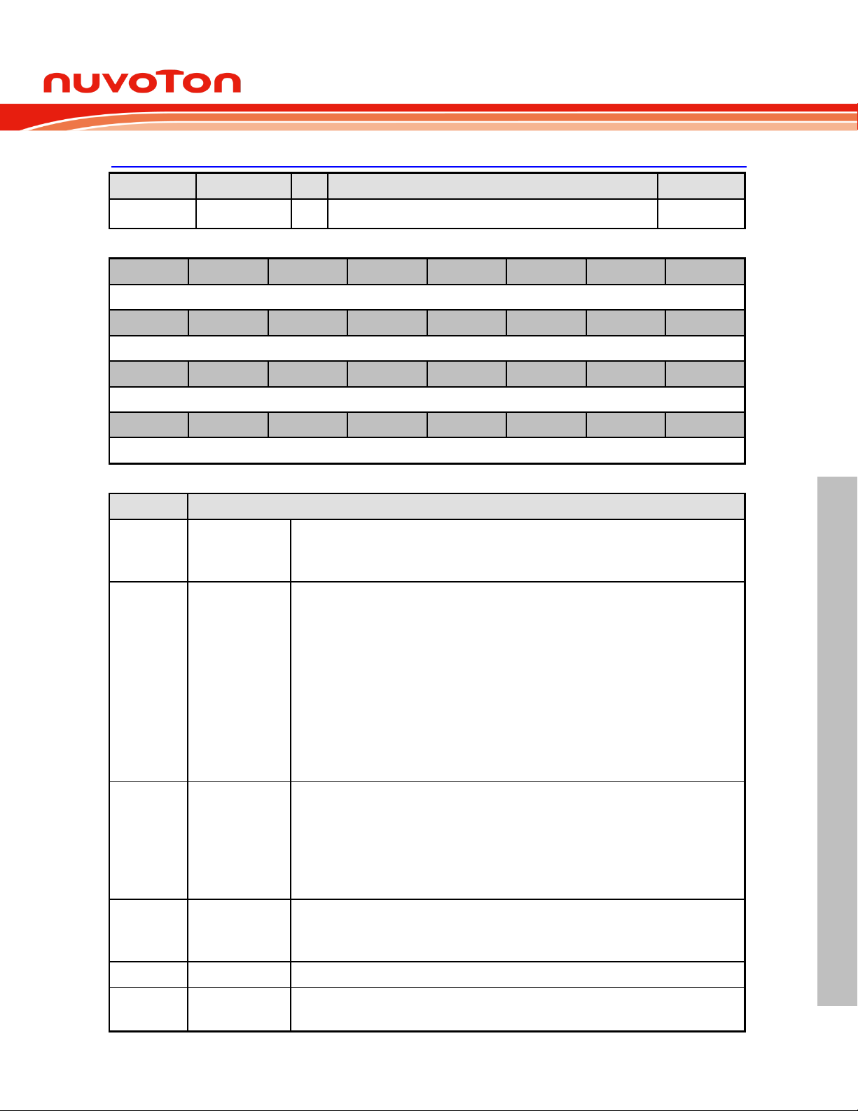
NuMicro® NUC029LEE/NUC029SEE
NUMICRO
®
NUC029LEE/NUC029SEE TECHNICAL REFERENCE MANUAL
Register
Offset
R/W
Description
Reset Value
GPB_MFP
GCR_BA+0x34
R/W
GPIOB Multiple Function and Input Type Control Register
0x0000_0000
31
30
29
28
27
26
25
24
GPB_TYPE
23
22
21
20
19
18
17
16
GPB_TYPE
15
14
13
12
11
10 9 8
GPB_MFP
7 6 5 4 3 2 1
0
GPB_MFP
Bits
Description
[31:16]
GPB_TYPEn
Trigger Function Selection
0 = GPIOB[15:0] I/O input Schmitt Trigger function Disabled.
1 = GPIOB[15:0] I/O input Schmitt Trigger function Enabled.
[15]
GPB_MFP15
PB.15 Pin Function Selection
Bits PB14_15_EBI (ALT_MFP2[1]), PB15_T0EX (ALT_MFP[24]), PB15_TM0
(ALT_MFP2[2]) and GPB_MFP[15] determine the PB.15 function.
(PB14_15_EBI, PB15_T0EX, PB15_TM0, GPB_MFP15) value and function mapping is as
following list.
(0, 0, 0, 0) = GPIO function is selected.
(0, 0, 0, 1) = INT1 function is selected.
(0 ,0, 1, 1) = TM0 function is selected.
(0, 1, 0, 0) = ADC11 function is selected.
(0, 1, 0, 1) = TM0_EXT function is selected.
(1, 0, 0, 1) = AD6 function is selected.
[14]
GPB_MFP14
PB.14 Pin Function Selection
Bits PB14_15_EBI (ALT_MFP2[1]) and GPB_MFP[14] determine the PB.14 function.
(PB14_15_EBI, GPB_MFP14) value and function mapping is as following list
(0, 0) = GPIO function is selected.
(0, 1) = INT0 function is selected.
(1, 1) = AD0 function is selected.
[13]
GPB_MFP13
PB.13 Pin Function Selection
0 = GPIO function is selected to the pin PB.13.
1 = AD1 function is selected.
[12]
GPB_MFP12
Reserved
[11]
GPB_MFP11
PB.11 Pin Function Selection
Bits PB11_PWM4 (ALT_MFP[4]) and GPB_MFP[11] determine the PB.11 function.
32-bit Arm® Cortex®-M0 Microcontroller
GPIOB Multiple Function Pin and Input Type Control Register (GPB_MFP)
Aug, 2018 Page 51 of 497 Rev 1.00
Page 52

NuMicro® NUC029LEE/NUC029SEE
NUMICRO
®
NUC029LEE/NUC029SEE TECHNICAL REFERENCE MANUAL
(PB11_PWM4, GPB_MFP11) value and function mapping is as following list.
(0, 0) = GPIO function is selected.
(0, 1) = TM3 function is selected.
(1, 1) = PWM4 function is selected.
[10]
GPB_MFP10
PB.10 Pin Function Selection
Bits PB10_S01 (ALT_MFP[0]) and GPB_MFP[10] determine the PB.10 function.
(PB10_S01, GPB_MFP10) value and function mapping is as following list.
(0, 0) = GPIO function is selected.
(0, 1) = TM2 function is selected.
(1, 1) = UART2_RXD function is selected.
[9]
GPB_MFP9
PB.9 Pin Function Selection
Bits PB9_S11 (ALT_MFP[1]) and GPB_MFP[9] determine the PB.9 function.
(PB9_S11, GPB_MFP9) value and function mapping is as following list.
(0, 0) = GPIO function is selected.
(0, 1) = TM1 function is selected.
(1, 1) = UART2_TXD function is selected.
[8]
GPB_MFP8
PB.8 Pin Function Selection
Bits PB8_CLKO (ALT_MFP[29]) and GPB_MFP[8] determine the PB.8 function.
(PB8_CLKO, GPB_MFP8) value and function mapping is as following list.
(0, 0) = GPIO function is selected.
(0, 1) = TM0 function is selected to the pin PB.8.
(1, 0) = STADC function is selected to the pin PB.8.
(1, 1) = CLKO function is selected to the pin PB.8.
[7]
GPB_MFP7
PB.7 Pin Function Selection
Bit EBI_EN (ALT_MFP[11]), GPB_MFP[7] determines the PB.7 function.
(EBI_EN, GPB_MFP7) value and function mapping is as following list.
(0, 0) = GPIO function is selected to the pin PB.7.
(0, 1) = UART1_nCTS function is selected to the pin PB.7.
(1, 1) = nCS(EBI) function is selected to the pin PB.7.
[6]
GPB_MFP6
PB.6 Pin Function Selection
Bit EBI_EN (ALT_MFP[11]), GPB_MFP[6] determines the PB.6 function.
(EBI_EN, GPB_MFP6) value and function mapping is as following list.
(0, 0) = GPIO function is selected to the pin PB.6.
(0, 1) = UART1_nRTS function is selected to the pin PB.6.
(1, 1) = ALE(EBI) function is selected to the pin PB.6.
[5]
GPB_MFP5
PB 5 Pin Function Selection
Bit GPB_MFP[5] determines the PB.5 function.
0 = GPIO function is selected to the pin PB.5.
1 = UART1_TXD function is selected to the pin PB.5.
[4]
GPB_MFP4
PB.4 Pin Function Selection
Bit GPB_MFP[4] determines the PB.4 function.
0 = GPIO function is selected to the pin PB.4.
1 = UART1_RXD function is selected to the pin PB.4.
[3]
GPB_MFP3
PB.3 Pin Function Selection
Bits EBI_nWRH_EN (ALT_MFP[14]), EBI_EN (ALT_MFP[11]), PB3_TM3 (ALT_MFP2[5]),
32-bit Arm® Cortex®-M0 Microcontroller
Aug, 2018 Page 52 of 497 Rev 1.00
Page 53

NuMicro® NUC029LEE/NUC029SEE
NUMICRO
®
NUC029LEE/NUC029SEE TECHNICAL REFERENCE MANUAL
PB3_T3EX (ALT_MFP[27]) and GPB_MFP[3] determine the PB.3 function.
(EBI_nWRH_EN, EBI_EN, PB3_TM3, PB3_T3EX, GPB_MFP3) value and function
mapping is as following list.
(0, 0, 0, 0, 0) = GPIO function is selected.
(0, 0, 0, 0, 1) = UART0_nCTS function is selected.
(0, 0, 0, 1, 1) = TM3_EXT function is selected.
(0, 0, 1, 0, 1) = TM3 function is selected.
(1, 1, 0, 0, 1) = nWRH(EBI) function is selected.
[2]
GPB_MFP2
PB.2 Pin Function Selection
Bits EBI_nWRL_EN (ALT_MFP[13]), EBI_EN (ALT_MFP[11]), PB2_TM2 (ALT_MFP2[4]),
PB2_T2EX (ALT_MFP[26]) and GPB_MFP[2] determine the PB.2 function.
(EBI_nWRL_EN, EBI_EN, PB2_TM2, PB2_T2EX, GPB_MFP2) value and function
mapping is as following list.
(0, 0, 0 , 0, 0) = GPIO function is selected.
(0, 0, 0, 0, 1) = UART0_nRTS function is selected.
(0, 0, 0, 1, 1) = TM2_EXT function is selected.
(0, 0, 1, 0, 1) = TM2 function is selected.
(1, 1, 0, 0, 1) = nWRL(EBI) function is selected.
[1]
GPB_MFP1
PB.1 Pin Function Selection
Bit GPB_MFP[1] determines the PB.1 function.
0 = GPIO function is selected to the pin PB.1.
1 = UART0_TXD function is selected to the pin PB.1.
[0]
GPB_MFP0
PB.0 Pin Function Selection
Bit GPB_MFP[0] determines the PB.0 function.
0 = GPIO function is selected to the pin PB.0.
1 = UART0_RXD function is selected to the pin PB.0.
32-bit Arm® Cortex®-M0 Microcontroller
Aug, 2018 Page 53 of 497 Rev 1.00
Page 54
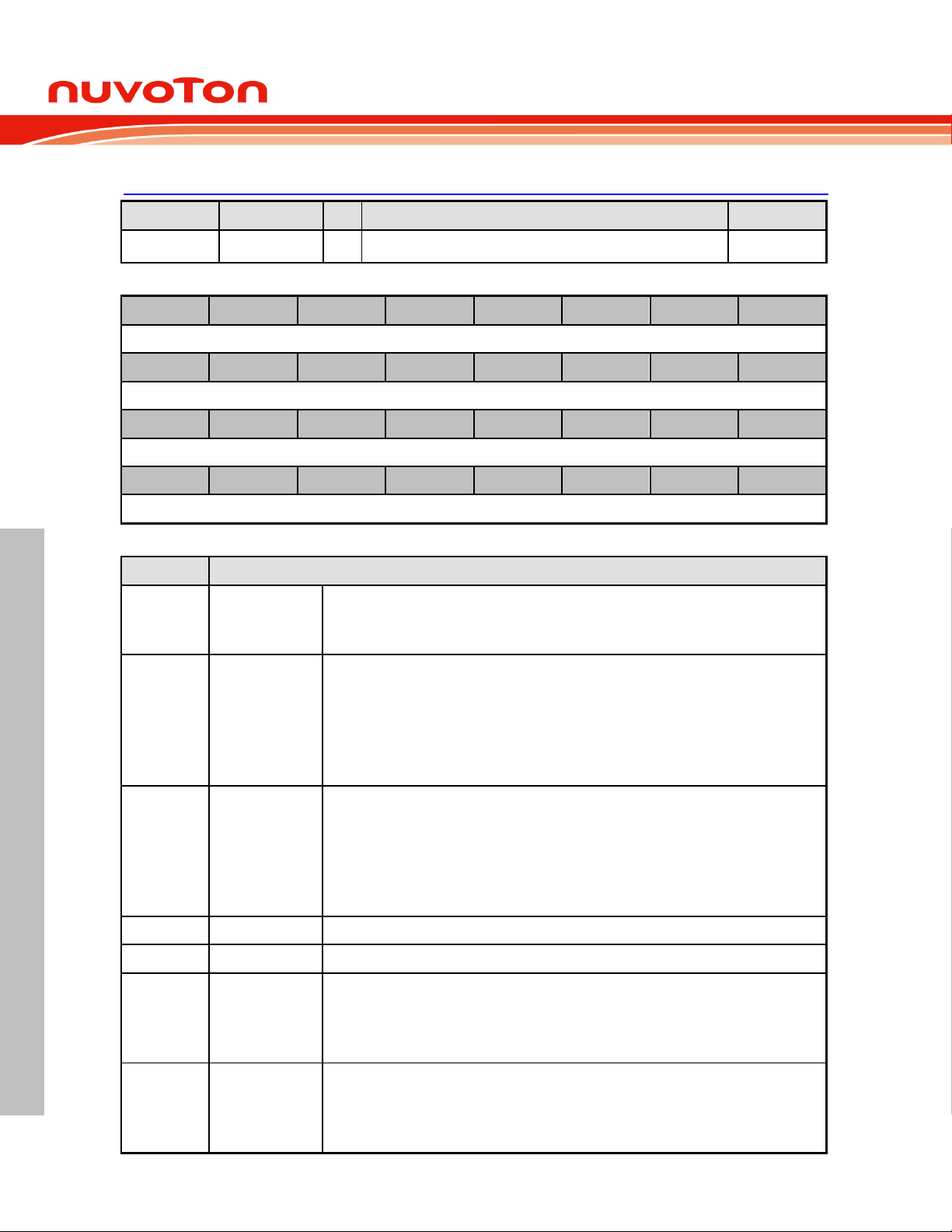
NuMicro® NUC029LEE/NUC029SEE
NUMICRO
®
NUC029LEE/NUC029SEE TECHNICAL REFERENCE MANUAL
Register
Offset
R/W
Description
Reset Value
GPC_MFP
GCR_BA+0x38
R/W
GPIOC Multiple Function and Input Type Control Register
0x0000_0000
31
30
29
28
27
26
25
24
GPC_TYPE
23
22
21
20
19
18
17
16
GPC_TYPE
15
14
13
12
11
10 9 8
GPC_MFP
7 6 5 4 3 2 1
0
GPC_MFP
Bits
Description
[31:16]
GPC_TYPEn
Trigger Function Selection
0 = GPIOC[15:0] I/O input Schmitt Trigger function Disabled.
1 = GPIOC[15:0] I/O input Schmitt Trigger function Enabled.
[15]
GPC_MFP15
PC.15 Pin Function Selection
Bits EBI_EN (ALT_MFP[11]) and GPC_MFP[15] determine the PC.15 function.
(EBI_EN, GPC_MFP15) value and function mapping is as following list
(0, 0) = GPIO function is selected.
(0, 1) = ADC9 function is selected.
(1, 1) = AD3 function is selected.
[14]
GPC_MFP14
PC.14 Pin Function Selection
Bits EBI_EN (ALT_MFP[11]) and GPC_MFP[14] determine the PC.14 function.
(EBI_EN, GPC_MFP14) value and function mapping is as following list
(0, 0) = GPIO function is selected.
(0, 1) = ADC10 function is selected.
(1, 1) = AD2 function is selected.
[13]
GPC_MFP13
Reserved
[12]
GPC_MFP12
Reserved
[11]
GPC_MFP11
PC.11 Pin Function Selection
Bit GPC_MFP[11] determines the PC.11 function.
0 = GPIO function is selected to the pin PC.11.
1 = SPI1_MOSI0 function is selected to the pin PC.11.
[10]
GPC_MFP10
PC.10 Pin Function Selection
Bit GPC_MFP[10] determines the PC.10 function.
0 = GPIO function is selected to the pin PC.10.
1 = SPI1_MISO0 function is selected to the pin PC.10.
32-bit Arm® Cortex®-M0 Microcontroller
GPIOC Multiple Function Pin and input Type Control Register (GPC_MFP)
Aug, 2018 Page 54 of 497 Rev 1.00
Page 55

NuMicro® NUC029LEE/NUC029SEE
NUMICRO
®
NUC029LEE/NUC029SEE TECHNICAL REFERENCE MANUAL
[9]
GPC_MFP9
PC.9 Pin Function Selection
Bit GPC_MFP[9] determines the PC.9 function.
0 = GPIO function is selected to the pin PC.9.
1 = SPI1_CLK function is selected to the pin PC.9.
[8]
GPC_MFP8
PC.8 Pin Function Selection
Bits EBI_MCLK_EN (ALT_MFP[12]), EBI_EN (ALT_MFP[11]), GPC_MFP[8] determine
the PC.8 function.
(EBI_MCLK_EN, EBI_EN, GPC_MFP8) value and function mapping is as following list.
(0, 0, 0) = GPIO function is selected to the pin PC.8.
(0, 0 ,1) = SPI1_SS0 function is selected to the pin PC.8.
(1, 1, 1) = MCLK(EBI) function is selected to the pin PC.8.
[7]
GPC_MFP7
PC.7 Pin Function Selection
Bits EBI_EN (ALT_MFP[11]) and GPC_MFP[7] determine the PC.7 function.
(EBI_EN, GPC_MFP7) value and function mapping is as following list.
(0, 0, 0) = GPIO function is selected.
(0, 0, 1) = ADC7 function is selected.
(1, 0, 1) = AD5 function is selected.
[6]
GPC_MFP6
PC.6 Pin Function Selection
Bits EBI_EN (ALT_MFP[11]) and GPC_MFP[6] determine the PC.6 function.
(EBI_EN, GPB_MFP6) value and function mapping is as following list.
(0, 0) = GPIO function is selected.
(0, 1) = ADC9 function is selected.
(1, 1) = AD4 function is selected.
[5]
GPC_MFP5
Reserved
[4]
GPC_MFP4
Reserved
[3]
GPC_MFP3
PC.3 Pin Function Selection
0 = GPIO function is selected.
1 = SPI0_MOSI0 function is selected.
[2]
GPC_MFP2
PC.2 Pin Function Selection
0 = GPIO function is selected.
1 = SPI0_MISO0 function is selected.
[1]
GPC_MFP1
PC.1 Pin Function Selection
0 = GPIO function is selected.
1 = SPI0_CLK function is selected.
[0]
GPC_MFP0
PC.0 Pin Function Selection
0 = GPIO function is selected.
1 = SPI0_SS0 function is selected.
32-bit Arm® Cortex®-M0 Microcontroller
Aug, 2018 Page 55 of 497 Rev 1.00
Page 56
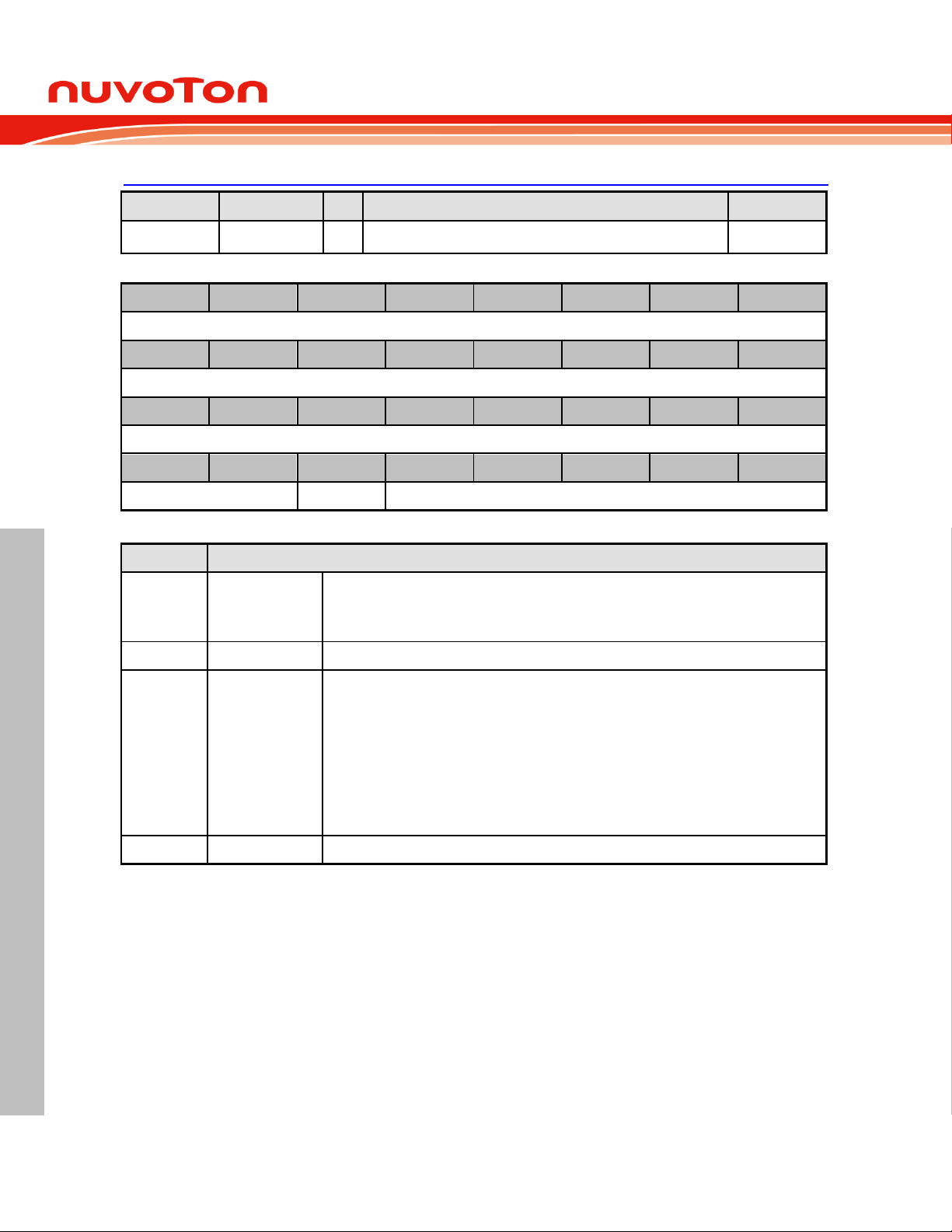
NuMicro® NUC029LEE/NUC029SEE
NUMICRO
®
NUC029LEE/NUC029SEE TECHNICAL REFERENCE MANUAL
Register
Offset
R/W
Description
Reset Value
GPE_MFP
GCR_BA+0x40
R/W
GPIOE Multiple Function and Input Type Control Register
0x0000_0000
31
30
29
28
27
26
25
24
GPE_TYPE
23
22
21
20
19
18
17
16
GPE_TYPE
15
14
13
12
11
10 9 8
Reserved
7 6 5 4 3 2 1
0
Reserved
GPE_MFP5
Reserved
Bits
Description
[31:16]
GPE_TYPEn
Trigger Function Selection
0 = GPIOE[15:0] I/O input Schmitt Trigger function Disabled.
1 = GPIOE[15:0] I/O input Schmitt Trigger function Enabled.
[15:6]
Reserved
Reserved.
[5]
GPE_MFP5
PE.5 Pin Function Selection
Bits PE5_T1EX (ALT_MFP[25]), PE5_TM1 (ALT_MFP2[3]) and GPE_MFP5 determine the
PE.5 function.
(PE5_T1EX, PE5_TM1, GPE_MFP5) value and function mapping is as following list.
(0, 0, 0) = GPIO function is selected.
(0, 0, 1) = PWM5 function is selected.
(1, 0, 1) = TM1_EXT function is selected.
(0, 1, 1) = TM1 function is selected.
[4:0]
Reserved
Reserved.
32-bit Arm® Cortex®-M0 Microcontroller
GPIOE Multiple Function Pin and Input Type Control Register (GPE_MFP)
Aug, 2018 Page 56 of 497 Rev 1.00
Page 57
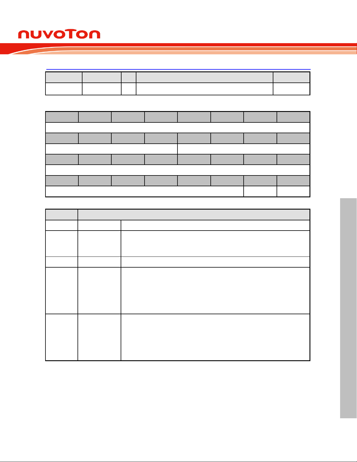
NuMicro® NUC029LEE/NUC029SEE
NUMICRO
®
NUC029LEE/NUC029SEE TECHNICAL REFERENCE MANUAL
Register
Offset
R/W
Description
Reset Value
GPF_MFP
GCR_BA+0x44
R/W
GPIOF Multiple Function and Input Type Control Register
0x0000_000X
31
30
29
28
27
26
25
24
Reserved
23
22
21
20
19
18
17
16
Reserved
GPF_TYPE
15
14
13
12
11
10 9 8
Reserved
7 6 5 4 3 2 1
0
Reserved
GPF_MFP1
GPF_MFP0
Bits
Description
[31:20]
Reserved
Reserved.
[19:16]
GPF_TYPEn
Trigger Function Selection
0 = GPIOF[3:0] I/O input Schmitt Trigger function Disabled.
1 = GPIOF[3:0] I/O input Schmitt Trigger function Enabled.
[15:2]
Reserved
Reserved.
[1]
GPF_MFP1
PF.1 Pin Function Selection
Bit GPF_MFP[1] determines the PF.1 function.
0 = GPIO function is selected to the pin PF.1.
1 = XT1_IN function is selected to the pin PF.1.
Note: This bit is read only and is decided by user configuration CGPFMFP
(CONFIG0[27]).
[0]
GPF_MFP0
PF.0 Pin Function Selection
Bit GPF_MFP[0] determines the PF.0 function
0 = GPIO function is selected to the pin PF.0.
1 = XT1_OUT function is selected to the pin PF.0.
Note: This bit is read only and is decided by user configuration CGPFMFP
(CONFIG0[27]).
32-bit Arm® Cortex®-M0 Microcontroller
GPIOF Multiple Function Pin and Input Type Control Register (GPF_MFP)
Note: The default value of GPF_MFP[3]/GPF_MFP[2] is 1. The default value of GPF_MFP[1]/GPF_MFP[0] is decided by user
configuration CGPFMFP(CONFIG0[27]).
Aug, 2018 Page 57 of 497 Rev 1.00
Page 58
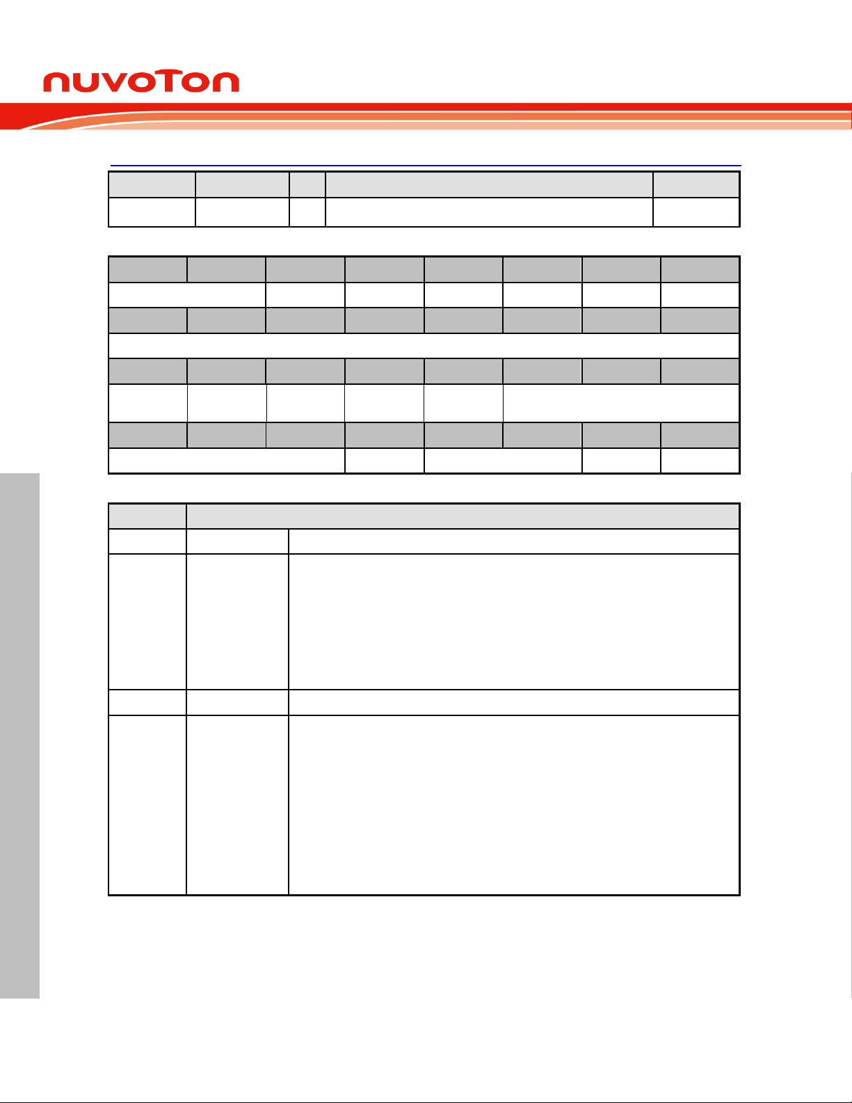
NuMicro® NUC029LEE/NUC029SEE
NUMICRO
®
NUC029LEE/NUC029SEE TECHNICAL REFERENCE MANUAL
Register
Offset
R/W
Description
Reset Value
ALT_MFP
GCR_BA+0x50
R/W
Alternative Multiple Function Pin Control Register
0x0000_0000
31
30
29
28
27
26
25
24
Reserved
PB8_CLKO
Reserved
PB3_T3EX
PB2_T2EX
PE5_T1EX
PB15_T0EX
23
22
21
20
19
18
17
16
EBI_HB_EN
15
14
13
12
11
10 9 8
Reserved
EBI_nWRH_E
N
EBI_nWRL_E
N
EBI_MCLK_E
N
EBI_EN
Reserved
7 6 5 4 3 2 1
0
Reserved
PB11_PWM4
Reserved
PB9_S11
PB10_S01
Bits
Description
[31:30]
Reserved
Reserved.
[29]
PB8_CLKO
PB.8 Pin Alternative Function Selection
Bits PB8_CLKO (ALT_MFP[29]) and GPB_MFP[8] determine the PB.8 function.
(PB8_CLKO, GPB_MFP8) value and function mapping is as following list.
(0, 0) = GPIO function is selected.
(0, 1) = TM0 function is selected to the pin PB.8.
(1, 0) = STADC function is selected to the pin PB.8.
(1, 1) = CLKO function is selected to the pin PB.8.
[28]
Reserved
Reserved.
[27]
PB3_T3EX
PB.3 Pin Alternative Function Selection
Bits EBI_nWRH_EN (ALT_MFP[14]), EBI_EN (ALT_MFP[11]), PB3_TM3 (ALT_MFP2[5]),
PB3_T3EX (ALT_MFP[27]) and GPB_MFP[3] determine the PB.3 function.
(EBI_nWRH_EN, EBI_EN, PB3_TM3, PB3_T3EX, GPB_MFP3) value and function
mapping is as following list.
(0, 0, 0, 0, 0) = GPIO function is selected.
(0, 0, 0, 0, 1) = UART0_nCTS function is selected.
(0, 0, 0, 1, 1) = TM3_EXT function is selected.
(0, 0, 1, 0, 1) = TM3 function is selected.
(1, 1, 0, 0, 1) = nWRH(EBI) function is selected.
32-bit Arm® Cortex®-M0 Microcontroller
Alternative Multiple Function Pin Control Register (ALT_MFP)
Aug, 2018 Page 58 of 497 Rev 1.00
Page 59

NuMicro® NUC029LEE/NUC029SEE
NUMICRO
®
NUC029LEE/NUC029SEE TECHNICAL REFERENCE MANUAL
[26]
PB2_T2EX
PB.2 Pin Alternative Function Selection
Bits EBI_nWRL_EN (ALT_MFP[13]), EBI_EN (ALT_MFP[11]), PB2_TM2 (ALT_MFP2[4]),
PB2_T2EX (ALT_MFP[26]) and GPB_MFP[2] determine the PB.2 function.
(EBI_nWRL_EN, EBI_EN, PB2_TM2, PB2_T2EX, GPB_MFP2) value and function
mapping is as following list.
(0, 0, 0 , 0, 0) = GPIO function is selected.
(0, 0, 0, 0, 1) = UART0_nRTS function is selected.
(0, 0, 0, 1, 1) = TM2_EXT function is selected.
(0, 0, 1, 0, 1) = TM2 function is selected.
(1, 1, 0, 0, 1) = nWRL(EBI) function is selected.
[25]
PE5_T1EX
PE.5 Pin Alternative Function Selection
Bits PE5_T1EX (ALT_MFP[25]), PE5_TM1 (ALT_MFP2[3]) and GPE_MFP5 determine the
PE.5 function.
(PE5_T1EX, PE5_TM1, GPE_MFP5) value and function mapping is as following list.
(0, 0, 0) = GPIO function is selected.
(0, 0, 1) = PWM5 function is selected.
(1, 0, 1) = TM1_EXT function is selected.
(0, 1, 1) = TM1 function is selected.
[24]
PB15_T0EX
PB.15 Pin Alternative Function Selection
Bits PB14_15_EBI (ALT_MFP2[1]), PB15_T0EX (ALT_MFP[24]), PB15_TM0
(ALT_MFP2[2]) and GPB_MFP[15] determine the PB.15 function.
(PB14_15_EBI, PB15_T0EX, PB15_TM0, GPB_MFP15) value and function mapping is as
following list.
(0, 0, 0, 0) = GPIO function is selected.
(0, 0, 0, 1) = INT1 function is selected.
(0 ,0, 1, 1) = TM0 function is selected.
(0, 1, 0, 0) = ADC11 function is selected.
(0, 1, 0, 1) = TM0_EXT function is selected.
(1, 0, 0, 1) = AD6 function is selected.
[23]
EBI_HB_EN[7]
Bits EBI_HB_EN[7] (ALT_MFP[23]), EBI_EN (ALT_MFP[11]) and GPA_MFP[14]
determine the PA.14 function.
(EBI_HB_EN, EBI_EN, GPA_MFP14) value and function mapping is as following list.
(0, 0, 0) = GPIO function is selected.
(0, 0, 1) = PWM2 function is selected.
(1, 1, 1) = AD15 function is selected.
[22]
EBI_HB_EN[6]
Bits EBI_HB_EN[6] (ALT_MFP[22]), EBI_EN (ALT_MFP[11]) and GPA_MFP[13]
determine the PA.13 function.
(EBI_HB_EN, EBI_EN, GPA_MFP13) value and function mapping is as following list.
(0, 0, 0) = GPIO function is selected.
(0, 0, 1) = PWM1 function is selected.
(1, 1, 1) = AD14 function is selected.
[21]
EBI_HB_EN[5]
Bits EBI_HB_EN[5] (ALT_MFP[21]), EBI_EN (ALT_MFP[11]) and GPA_MFP[12]
determine the PA.12 function.
(EBI_HB_EN, EBI_EN, GPA_MFP12) value and function mapping is as following list.
(0, 0, 0) = GPIO function is selected.
(0, 0, 1) = PWM0 function is selected.
(1, 1, 1) = AD13 function is selected.
32-bit Arm® Cortex®-M0 Microcontroller
Aug, 2018 Page 59 of 497 Rev 1.00
Page 60

NuMicro® NUC029LEE/NUC029SEE
NUMICRO
®
NUC029LEE/NUC029SEE TECHNICAL REFERENCE MANUAL
[20]
EBI_HB_EN[4]
Bit EBI_HB_EN[4] (ALT_MFP[20]), EBI_EN (ALT_MFP[11]) and GPA_MFP[1] determine
the PA.1 function.
(EBI_HB_EN, EBI_EN, GPA_MFP1) value and function mapping is as following list.
(0, 0, 0) = GPIO function is selected.
(0, 0, 1) = ADC1 function is selected.
(1, 1, 1) = AD12 function is selected.
[19]
EBI_HB_EN[3]
Bits EBI_HB_EN[3] (ALT_MFP[19]), EBI_EN (ALT_MFP[11]) and GPA_MFP[2] determine
the PA.2 function.
(EBI_HB_EN, EBI_EN, GPA_MFP2) value and function mapping is as following list.
(0, 0, 0) = GPIO function is selected.
(0, 0, 1) = ADC2 function is selected.
(1, 1, 1) = AD11 function is selected.
[18]
EBI_HB_EN[2]
Bits EBI_HB_EN[2] (ALT_MFP[18]), EBI_EN (ALT_MFP[11]) and GPA_MFP[3] determine
the PA.3 function.
(EBI_HB_EN, EBI_EN, GPA_MFP3) value and function mapping is as following list.
(0, 0, 0) = GPIO function is selected.
(0, 0, 1) = ADC3 function is selected.
(1, 1, 1) = AD10 function is selected.
[17]
EBI_HB_EN[1]
Bits EBI_HB_EN[1] (ALT_MFP[17]), EBI_EN (ALT_MFP[11]) and GPA_MFP[4] determine
the PA.4 function.
(EBI_HB_EN, EBI_EN, GPA_MFP4) value and function mapping is as following list.
(0, 0, 0) = GPIO function is selected.
(0, 0, 1) = ADC4 function is selected.
(1, 1, 1) = AD9 function is selected.
[16]
EBI_HB_EN[0]
Bits EBI_HB_EN[0] (ALT_MFP[16]), EBI_EN (ALT_MFP[11]) and GPA_MFP[5] determine
the PA.5 function.
(EBI_HB_EN, EBI_EN, GPA_MFP5) value and function mapping is as following list,
(0, 0, 0) = GPIO function is selected.
(0, 0, 1) = ADC5 function is selected.
(1, 1, 1) = AD8 function is selected.
[15]
Reserved
Reserved
[14]
EBI_nWRH_EN
Bits EBI_nWRH_EN (ALT_MFP[14]), EBI_EN (ALT_MFP[11]), PB3_TM3 (ALT_MFP2[5]),
PB3_T3EX (ALT_MFP[27]) and GPB_MFP[3] determine the PB.3 function.
(EBI_nWRH_EN, EBI_EN, PB3_TM3, PB3_T3EX, GPB_MFP3) value and function
mapping is as following list.
(0, 0, 0, 0, 0) = GPIO function is selected.
(0, 0, 0, 0, 1) = UART0_nCTS function is selected.
(0, 0, 0, 1, 1) = TM3_EXT function is selected.
(0, 0, 1, 0, 1) = TM3 function is selected.
(1, 1, 0, 0, 1) = nWRH(EBI) function is selected.
32-bit Arm® Cortex®-M0 Microcontroller
Aug, 2018 Page 60 of 497 Rev 1.00
Page 61

NuMicro® NUC029LEE/NUC029SEE
NUMICRO
®
NUC029LEE/NUC029SEE TECHNICAL REFERENCE MANUAL
[13]
EBI_nWRL_EN
Bits EBI_nWRL_EN (ALT_MFP[13]), EBI_EN (ALT_MFP[11]), PB2_TM2 (ALT_MFP2[4]),
PB2_T2EX (ALT_MFP[26]) and GPB_MFP[2] determine the PB.2 function.
(EBI_nWRL_EN, EBI_EN, PB2_TM2, PB2_T2EX, GPB_MFP2) value and function
mapping is as following list.
(0, 0, 0 , 0, 0) = GPIO function is selected.
(0, 0, 0, 0, 1) = UART0_nRTS function is selected.
(0, 0, 0, 1, 1) = TM2_EXT function is selected.
(0, 0, 1, 0, 1) = TM2 function is selected.
(1, 1, 0, 0, 1) = nWRL(EBI) function is selected.
[12]
EBI_MCLK_EN
Bits EBI_MCLK_EN (ALT_MFP[12]), EBI_EN (ALT_MFP[11]), GPC_MFP[8] determine
the PC.8 function.
(EBI_MCLK_EN, EBI_EN, GPC_MFP8) value and function mapping is as following list.
(0, 0, 0) = GPIO function is selected to the pin PC.8.
(0, 0 ,1) = SPI1_SS0 function is selected to the pin PC.8.
(1, 1, 1) = MCLK(EBI) function is selected to the pin PC.8.
[11]
EBI_EN
EBI_EN is use to switch GPIO function to EBI function (AD[15:0], ALE, RE, WE, CS,
MCLK), it need additional registers EBI_EN[7:0] and EBI_MCLK_EN for some GPIO to
switch to EBI function(AD[15:8], MCLK)
[10:5]
Reserved
Reserved
[4]
PB11_PWM4
PB.11 Pin Alternative Function Selection
Bits PB11_PWM4 (ALT_MFP[4]) and GPB_MFP[11] determine the PB.11 function.
(PB11_PWM4, GPB_MFP11) value and function mapping is as following list.
(0, 0) = GPIO function is selected.
(0, 1) = TM3 function is selected.
(1, 1) = PWM4 function is selected.
[3]
PB14_S31
PB.14 Pin Alternative Function Selection
Bits PB14_15_EBI (ALT_MFP2[1]) and GPB_MFP[14] determine the PB.14 function.
(PB14_15_EBI, GPB_MFP14) value and function mapping is as following list
(0, 0) = GPIO function is selected.
(0, 1) = INT0 function is selected.
(1, 1) = AD0 function is selected.
[2]
Reserved
Reserved
[1]
PB9_S11
PB.9 Pin Alternative Function Selection
Bits PB9_S11 (ALT_MFP[1]) and GPB_MFP[9] determine the PB.9 function.
(PB9_S11, GPB_MFP9) value and function mapping is as following list.
(0, 0) = GPIO function is selected.
(0, 1) = TM1 function is selected.
(1, 1) = UART2_TXD function is selected.
[0]
PB10_S01
PB.10 Pin Alternative Function Selection
Bits PB10_S01 (ALT_MFP[0]) and GPB_MFP[10] determine the PB.10 function.
(PB10_S01, GPB_MFP10) value and function mapping is as following list.
(0, 0) = GPIO function is selected.
(0, 1) = TM2 function is selected.
(1, 1) = UART2_RXD function is selected.
32-bit Arm® Cortex®-M0 Microcontroller
Aug, 2018 Page 61 of 497 Rev 1.00
Page 62
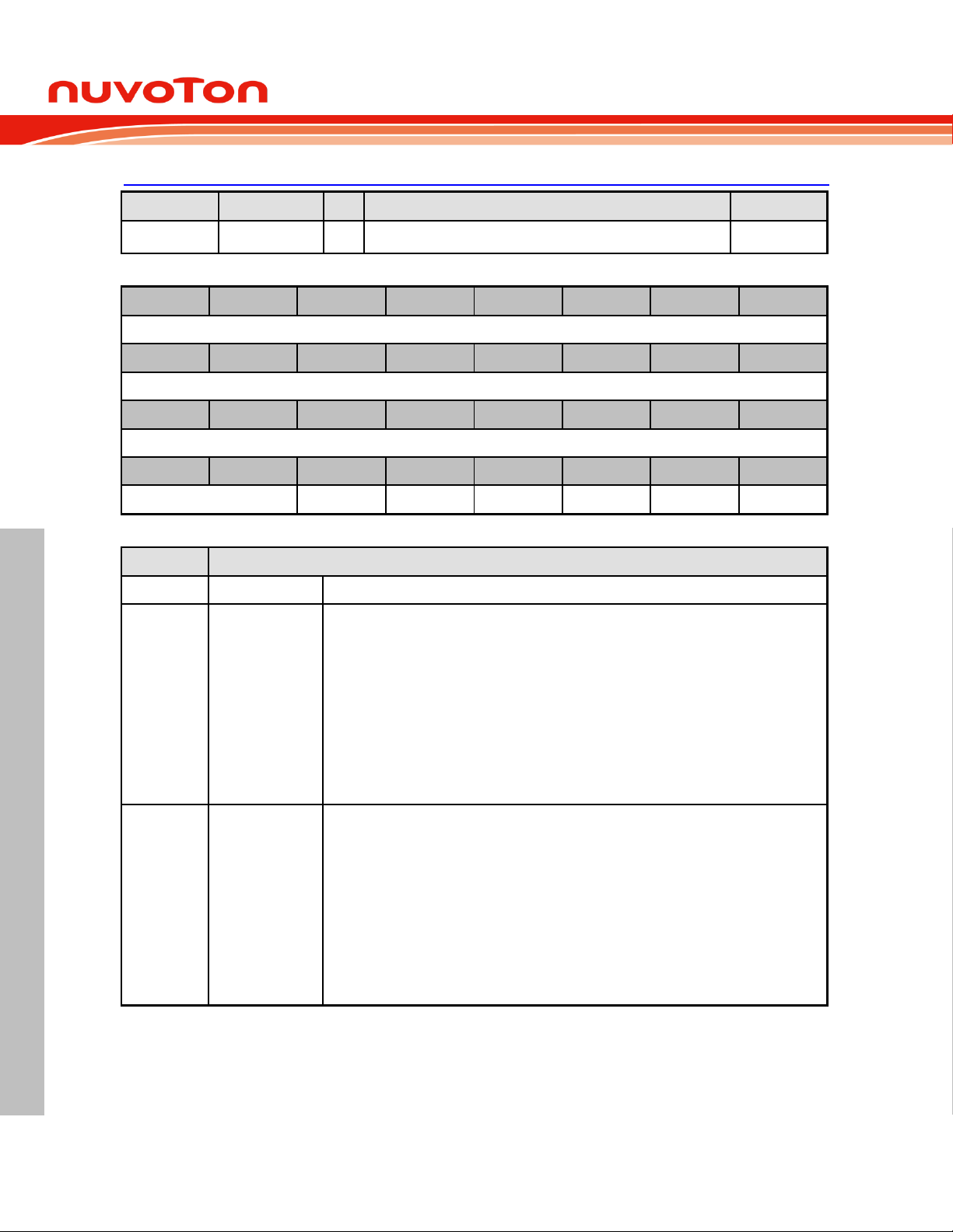
NuMicro® NUC029LEE/NUC029SEE
NUMICRO
®
NUC029LEE/NUC029SEE TECHNICAL REFERENCE MANUAL
Register
Offset
R/W
Description
Reset Value
ALT_MFP2
GCR_BA+0x5C
R/W
Alternative Multiple Function Pin Control Register 2
0x0000_0000
31
30
29
28
27
26
25
24
Reserved
23
22
21
20
19
18
17
16
Reserved
15
14
13
12
11
10 9 8
Reserved
7 6 5 4 3 2 1
0
Reserved
PB3_TM3
PB2_TM2
PE5_TM1
PB15_TM0
PB14_15_EBI
Reserved
Bits
Description
[31:6]
Reserved
Reserved.
[5]
PB3_TM3
PB.3 Pin Alternative Function Selection
Bits EBI_nWRH_EN (ALT_MFP[14]), EBI_EN (ALT_MFP[11]), PB3_TM3 (ALT_MFP2[5]),
PB3_T3EX (ALT_MFP[27]) and GPB_MFP[3] determine the PB.3 function.
(EBI_nWRH_EN, EBI_EN, PB3_TM3, PB3_T3EX, GPB_MFP3) value and function
mapping is as following list.
(0, 0, 0, 0, 0) = GPIO function is selected.
(0, 0, 0, 0, 1) = UART0_nCTS function is selected.
(0, 0, 0, 1, 1) = TM3_EXT function is selected.
(0, 0, 1, 0, 1) = TM3 function is selected.
(1, 1, 0, 0, 1) = nWRH(EBI) function is selected.
[4]
PB2_TM2
PB.2 Pin Alternative Function Selection
Bits EBI_nWRL_EN (ALT_MFP[13]), EBI_EN (ALT_MFP[11]), PB2_TM2 (ALT_MFP2[4]),
PB2_T2EX (ALT_MFP[26]) and GPB_MFP[2] determine the PB.2 function.
(EBI_nWRL_EN, EBI_EN, PB2_TM2, PB2_T2EX, GPB_MFP2) value and function
mapping is as following list.
(0, 0, 0 , 0, 0) = GPIO function is selected.
(0, 0, 0, 0, 1) = UART0_nRTS function is selected.
(0, 0, 0, 1, 1) = TM2_EXT function is selected.
(0, 0, 1, 0, 1) = TM2 function is selected.
(1, 1, 0, 0, 1) = nWRL(EBI) function is selected.
32-bit Arm® Cortex®-M0 Microcontroller
Alternative Multiple Function Pin Control Register 2 (ALT_MFP2)
Aug, 2018 Page 62 of 497 Rev 1.00
Page 63

NuMicro® NUC029LEE/NUC029SEE
NUMICRO
®
NUC029LEE/NUC029SEE TECHNICAL REFERENCE MANUAL
[3]
PE5_TM1
PE.5 Pin Alternative Function Selection
Bits PE5_T1EX (ALT_MFP[25]), PE5_TM1 (ALT_MFP2[3]) and GPE_MFP5 determine the
PE.5 function.
(PE5_T1EX, PE5_TM1, GPE_MFP5) value and function mapping is as following list.
(0, 0, 0) = GPIO function is selected.
(0, 0, 1) = PWM5 function is selected.
(1, 0, 1) = TM1_EXT function is selected.
(0, 1, 1) = TM1 function is selected.
[2]
PB15_TM0
PB.15 Pin Alternative Function Selection
Bits PB14_15_EBI (ALT_MFP2[1]), PB15_T0EX (ALT_MFP[24]), PB15_TM0
(ALT_MFP2[2]) and GPB_MFP[15] determine the PB.15 function.
(PB14_15_EBI, PB15_T0EX, PB15_TM0, GPB_MFP15) value and function mapping is as
following list.
(0, 0, 0, 0) = GPIO function is selected.
(0, 0, 0, 1) = INT1 function is selected.
(0 ,0, 1, 1) = TM0 function is selected.
(0, 1, 0, 0) = ADC11 function is selected.
(0, 1, 0, 1) = TM0_EXT function is selected.
(1, 0, 0, 1) = AD6 function is selected.
[1]
PB14_15_EBI
PB .14 and PB.15 Pin Alternative Function Selection
Bits PB14_15_EBI (ALT_MFP2[1]), PB15_T0EX (ALT_MFP[24]), PB15_TM0
(ALT_MFP2[2]) and GPB_MFP[15] determine the PB.15 function.
(PB14_15_EBI, PB15_T0EX, PB15_TM0, GPB_MFP15) value and function mapping is as
following list.
(0, 0, 0, 0) = GPIO function is selected.
(0, 0, 0, 1) = INT1 function is selected.
(0 ,0, 1, 1) = TM0 function is selected.
(0, 1, 0, 0) = ADC11 function is selected.
(0, 1, 0, 1) = TM0_EXT function is selected.
(1, 0, 0, 1) = AD6 function is selected.
Bits PB14_15_EBI (ALT_MFP2[1]) and GPB_MFP[14] determine the PB.14 function.
(PB14_15_EBI, GPB_MFP14) value and function mapping is as following list
(0, 0) = GPIO function is selected.
(0, 1) = INT0 function is selected.
(1, 1) = AD0 function is selected.
[0]
Reserved
Reserved.
32-bit Arm® Cortex®-M0 Microcontroller
Aug, 2018 Page 63 of 497 Rev 1.00
Page 64
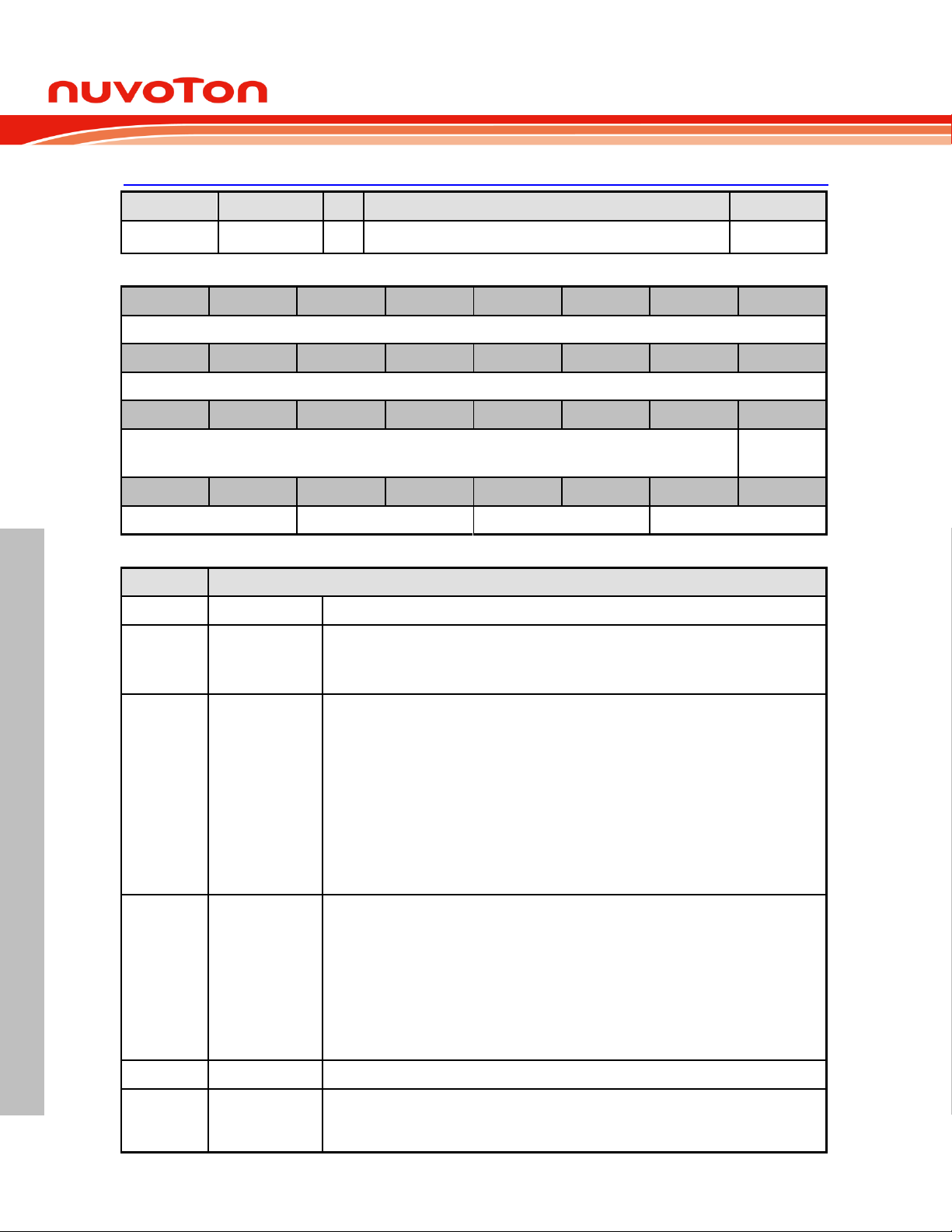
NuMicro® NUC029LEE/NUC029SEE
NUMICRO
®
NUC029LEE/NUC029SEE TECHNICAL REFERENCE MANUAL
Register
Offset
R/W
Description
Reset Value
IRCTCTL
GCR_BA+0x80
R/W
IRC Trim Control Register
0x0000_0000
31
30
29
28
27
26
25
24
Reserved
23
22
21
20
19
18
17
16
Reserved
15
14
13
12
11
10 9 8
Reserved
CLKERR_
STOP_EN
7 6 5 4 3 2 1
0
TRIM_RETRY_CNT
TRIM_LOOP
Reserved
TRIM_SEL
Bits
Description
[31:9]
Reserved
Reserved.
[8]
CLKERR_STOP_E
N
Clock Error Stop Enable Bit
0 = The trim operation is kept going if clock is inaccuracy.
1 = The trim operation is stopped if clock is inaccuracy.
[7:6]
TRIM_RETRY_CN
T
Trim Value Update Limitation Count
The field defines that how many times of HIRC trim value is updated by auto trim circuit
before the HIRC frequency locked.
Once the HIRC locked, the internal trim value update counter will be reset.
If the trim value update counter reached this limitation value and frequency of HIRC still
doesn’t lock, the auto trim operation will be disabled and TRIM_SEL will be cleared to 00.
00 = Trim retry count limitation is 64.
01 = Trim retry count limitation is 128.
10 = Trim retry count limitation is 256.
11 = Trim retry count limitation is 512.
[5:4]
TRIM_LOOP
Trim Calculation Loop
This field defines that trim value calculation is based on how many 32.768 kHz clocks in.
For example, if TRIM_LOOP is set as 00, auto trim circuit will calculate trim value based
on the average frequency difference in 4 32.768 kHz clock.
00 = Trim value calculation is based on average difference in 4 clocks.
01 = Trim value calculation is based on average difference in 8 clocks.
10 = Trim value calculation is based on average difference in 16 clocks.
11 = Trim value calculation is based on average difference in 32 clocks.
[3:2]
Reserved
Reserved.
[1:0]
TRIM_SEL
Trim Frequency Selection
This field indicates the target frequency of internal 22.1184 MHz high speed oscillator will
trim to precise 22.1184MHz or 24MHz automatically.
32-bit Arm® Cortex®-M0 Microcontroller
IRC Trim Control Register (SYS_IRCTCTL)
Aug, 2018 Page 64 of 497 Rev 1.00
Page 65
NUMICRO
®
NUC029LEE/NUC029SEE TECHNICAL REFERENCE MANUAL
If no any target frequency is selected (TRIM_SEL is 00), the HIRC auto trim function is
disabled.
During auto trim operation, if clock error detected because of CLKERR_STOP_EN is set to
1 or trim retry limitation counts reached, this field will be cleared to 00 automatically.
00 = HIRC auto trim function Disabled.
01 = HIRC auto trim function Enabled and HIRC trimmed to 22.1184 MHz.
10 = HIRC auto trim function Enabled and HIRC trimmed to 24 MHz.
11 = Reserved.
NuMicro® NUC029LEE/NUC029SEE
32-bit Arm® Cortex®-M0 Microcontroller
Aug, 2018 Page 65 of 497 Rev 1.00
Page 66
NuMicro® NUC029LEE/NUC029SEE
NUMICRO
®
NUC029LEE/NUC029SEE TECHNICAL REFERENCE MANUAL
Register
Offset
R/W
Description
Reset Value
IRCTIEN
GCR_BA+0x84
R/W
IRC Trim Interrupt Enable Register
0x0000_0000
31
30
29
28
27
26
25
24
Reserved
23
22
21
20
19
18
17
16
Reserved
15
14
13
12
11
10 9 8
Reserved
7 6 5 4 3 2 1
0
Reserved
CLKERR_IEN
TRIM_FAIL_
IEN
Reserved
Bits
Description
[31:3]
Reserved
Reserved.
[2]
CLKERR_IEN
Clock Error Interrupt Enable Bit
This bit controls if CPU would get an interrupt while clock is inaccuracy during auto trim
operation.
If this bit is set to1, and CLKERR_INT (IRCTRIMINT[2]) is set during auto trim operation.
An interrupt will be triggered to notify the clock frequency is inaccuracy.
0 = CLKERR_INT (IRCTRIMINT[2]) status to trigger an interrupt to CPU Disabled.
1 = CLKERR_INT (IRCTRIMINT[2]) status to trigger an interrupt to CPU Enabled.
[1]
TRIM_FAIL_IEN
Trim Failure Interrupt Enable Bit
This bit controls if an interrupt will be triggered while HIRC trim value update limitation
count reached and HIRC frequency still not locked on target frequency set by TRIM_SEL
(IRCTCTL[1:0]).
If this bit is high and TRIM_FAIL_INT (IRCTRIMINT[1]) is set during auto trim operation.
An interrupt will be triggered to notify that HIRC trim value update limitation count was
reached.
0 = TRIM_FAIL_INT (IRCTRIMINT[1]) status to trigger an interrupt to CPU Disabled.
1 = TRIM_FAIL_INT (IRCTRIMINT[1]) status to trigger an interrupt to CPU Enabled.
[0]
Reserved
Reserved.
32-bit Arm® Cortex®-M0 Microcontroller
IRC Trim Interrupt Enable Register (SYS_IRCTIEN)
Aug, 2018 Page 66 of 497 Rev 1.00
Page 67
NuMicro® NUC029LEE/NUC029SEE
NUMICRO
®
NUC029LEE/NUC029SEE TECHNICAL REFERENCE MANUAL
Register
Offset
R/W
Description
Reset Value
IRCTSTS
GCR_BA+0x88
R/W
IRC Trim Interrupt Status Register
0x0000_0000
31
30
29
28
27
26
25
24
Reserved
23
22
21
20
19
18
17
16
Reserved
15
14
13
12
11
10 9 8
Reserved
7 6 5 4 3 2 1
0
Reserved
CLKERR_INT
TRIM_FAIL_
INT
FREQ_LOCK
Bits
Description
[31:3]
Reserved
Reserved.
[2]
CLKERR_INT
Clock Error Interrupt Status
When the frequency of external 32.768 kHz low speed crystal or internal 22.1184 MHz
high speed oscillator is shift larger to unreasonable value, this bit will be set and to be an
indicate that clock frequency is inaccuracy
Once this bit is set to 1, the auto trim operation stopped and TRIM_SEL (IRCTCTL[1:0])
will be cleared to 00 by hardware automatically if CLKERR_STOP_EN (IRCTCTL[8]) is set
to 1.
If this bit is set and CLKERR_IEN (IRCTIEN [2]) is high, an interrupt will be triggered to
notify the clock frequency is inaccuracy. Write 1 to clear this to 0.
0 = Clock frequency is accurate.
1 = Clock frequency is inaccurate.
[1]
TRIM_FAIL_INT
Trim Failure Interrupt Status
This bit indicates that internal 22.1184 MHz high speed oscillator trim value update
limitation count reached and the internal 22.1184 MHz high speed oscillator clock
frequency still doesn’t be locked. Once this bit is set, the auto trim operation stopped and
TRIM_SEL (IRCTCTL[1:0]) will be cleared to 00 by hardware automatically.
If this bit is set and TRIM_FAIL_IEN (IRCTIEN[1]) is high, an interrupt will be triggered to
notify that HIRC trim value update limitation count was reached. Write 1 to clear this to 0.
0 = Trim value update limitation count did not reach.
1 = Trim value update limitation count reached and internal 22.1184 MHz high speed
oscillator frequency was still not locked.
[0]
FREQ_LOCK
HIRC Frequency Lock Status
This bit indicates the internal 22.1184 MHz high speed oscillator frequency is locked.
This is a status bit and doesn’t trigger any interrupt.
32-bit Arm® Cortex®-M0 Microcontroller
IRC Trim Interrupt Status Register (SYS_IRCTSTS)
Aug, 2018 Page 67 of 497 Rev 1.00
Page 68
NuMicro® NUC029LEE/NUC029SEE
NUMICRO
®
NUC029LEE/NUC029SEE TECHNICAL REFERENCE MANUAL
Register
Offset
R/W
Description
Reset Value
HIRCTCTL
GCR_BA+0x90
R/W
HIRC Trim Control Register
0x0008_0000
31
30
29
28
27
26
25
24
Reserved
23
22
21
20
19
18
17
16
Reserved
BOUNDARY
15
14
13
12
11
10 9 8
Reserved
BOUNDEN
CESTOPEN
7 6 5 4 3 2 1 0 RETRYCNT
LOOPSEL
Reserved
FREQSEL
Bits
Description
[31:21]
Reserved
Reserved.
[20:16]
BOUNDARY
Boundary Selection
Fill the boundary range from 1 to 31, 0 is reserved.
Note: This field is effective only when the BOUNDEN(SYS_HIRCTCTL[9]) is enable.
[15:10]
Reserved
Reserved.
[9]
BOUNDEN
Boundary Enable
0 = Boundary function is disable.
1 = Boundary function is enable.
[8]
CESTOPEN
Clock Error Stop Enable Bit
0 = The trim operation is keep going if clock is inaccuracy.
1 = The trim operation is stopped if clock is inaccuracy.
[7:6]
RETRYCNT
Trim Value Update Limitation Count
This field defines that how many times the auto trim circuit will try to update the HIRC trim
value before the frequency of HIRC locked.
Once the HIRC locked, the internal trim value update counter will be reset.
If the trim value update counter reached this limitation value and frequency of HIRC still
doesn’t lock, the auto trim operation will be disabled and FREQSEL will be cleared to 00.
00 = Trim retry count limitation is 64 loops.
01 = Trim retry count limitation is 128 loops.
10 = Trim retry count limitation is 256 loops.
11 = Trim retry count limitation is 512 loops.
[5:4]
LOOPSEL
Trim Calculation Loop Selection
This field defines that trim value calculation is based on how many reference clocks.
00 = Trim value calculation is based on average difference in 4 clocks of reference clock.
01 = Trim value calculation is based on average difference in 8 clocks of reference clock.
32-bit Arm® Cortex®-M0 Microcontroller
HIRC Trim Control Register (SYS_HIRCTCTL)
Aug, 2018 Page 68 of 497 Rev 1.00
Page 69

NUMICRO
®
NUC029LEE/NUC029SEE TECHNICAL REFERENCE MANUAL
10 = Trim value calculation is based on average difference in 16 clocks of reference clock.
11 = Trim value calculation is based on average difference in 32 clocks of reference clock.
Note: For example, if LOOPSEL is set as 00, auto trim circuit will calculate trim value
based on the average frequency difference in 4 clocks of reference clock.
[3:2]
Reserved
Reserved.
[1:0]
FREQSEL
Trim Frequency Selection
This field indicates the target frequency of 48 MHz internal high speed RC oscillator
(HIRC) auto trim.
During auto trim operation, if clock error detected with CESTOPEN is set to 1 or trim retry
limitation count reached, this field will be cleared to 00 automatically.
00 = Disable HIRC auto trim function.
01 = Enable HIRC auto trim function and trim HIRC to 48 MHz.
10 = Reserved.
11 = Reserved.
NuMicro® NUC029LEE/NUC029SEE
32-bit Arm® Cortex®-M0 Microcontroller
Aug, 2018 Page 69 of 497 Rev 1.00
Page 70
NuMicro® NUC029LEE/NUC029SEE
NUMICRO
®
NUC029LEE/NUC029SEE TECHNICAL REFERENCE MANUAL
Register
Offset
R/W
Description
Reset Value
HIRCTIEN
GCR_BA+0x94
R/W
HIRC Trim Interrupt Enable Register
0x0000_0000
31
30
29
28
27
26
25
24
Reserved
23
22
21
20
19
18
17
16
Reserved
15
14
13
12
11
10 9 8
Reserved
7 6 5 4 3 2 1
0
Reserved
CLKEIEN
TFALIEN
Reserved
Bits
Description
[31:3]
Reserved
Reserved.
[2]
CLKEIEN
Clock Error Interrupt Enable Bit
This bit controls if CPU would get an interrupt while clock is inaccuracy during auto trim
operation.
If this bit is set to1, and CLKERRIF(SYS_HIRCTSTS[2]) is set during auto trim operation,
an interrupt will be triggered to notify the clock frequency is inaccuracy.
0 = Disable CLKERRIF(SYS_HIRCTSTS[2]) status to trigger an interrupt to CPU.
1 = Enable CLKERRIF(SYS_HIRCTSTS[2]) status to trigger an interrupt to CPU.
[1]
TFALIEN
Trim Failure Interrupt Enable Bit
This bit controls if an interrupt will be triggered while HIRC trim value update limitation
count reached and HIRC frequency still not locked on target frequency set by
FREQSEL(SYS_HIRCTCTL[1:0]).
If this bit is high and TFAILIF(SYS_HIRCTSTS[1]) is set during auto trim operation, an
interrupt will be triggered to notify that HIRC trim value update limitation count was
reached.
0 = Disable TFAILIF(SYS_HIRCTSTS[1]) status to trigger an interrupt to CPU.
1 = Enable TFAILIF(SYS_HIRCTSTS[1]) status to trigger an interrupt to CPU.
[0]
Reserved
Reserved.
32-bit Arm® Cortex®-M0 Microcontroller
HIRC Trim Interrupt Enable Register (SYS_HIRCTIEN)
Aug, 2018 Page 70 of 497 Rev 1.00
Page 71
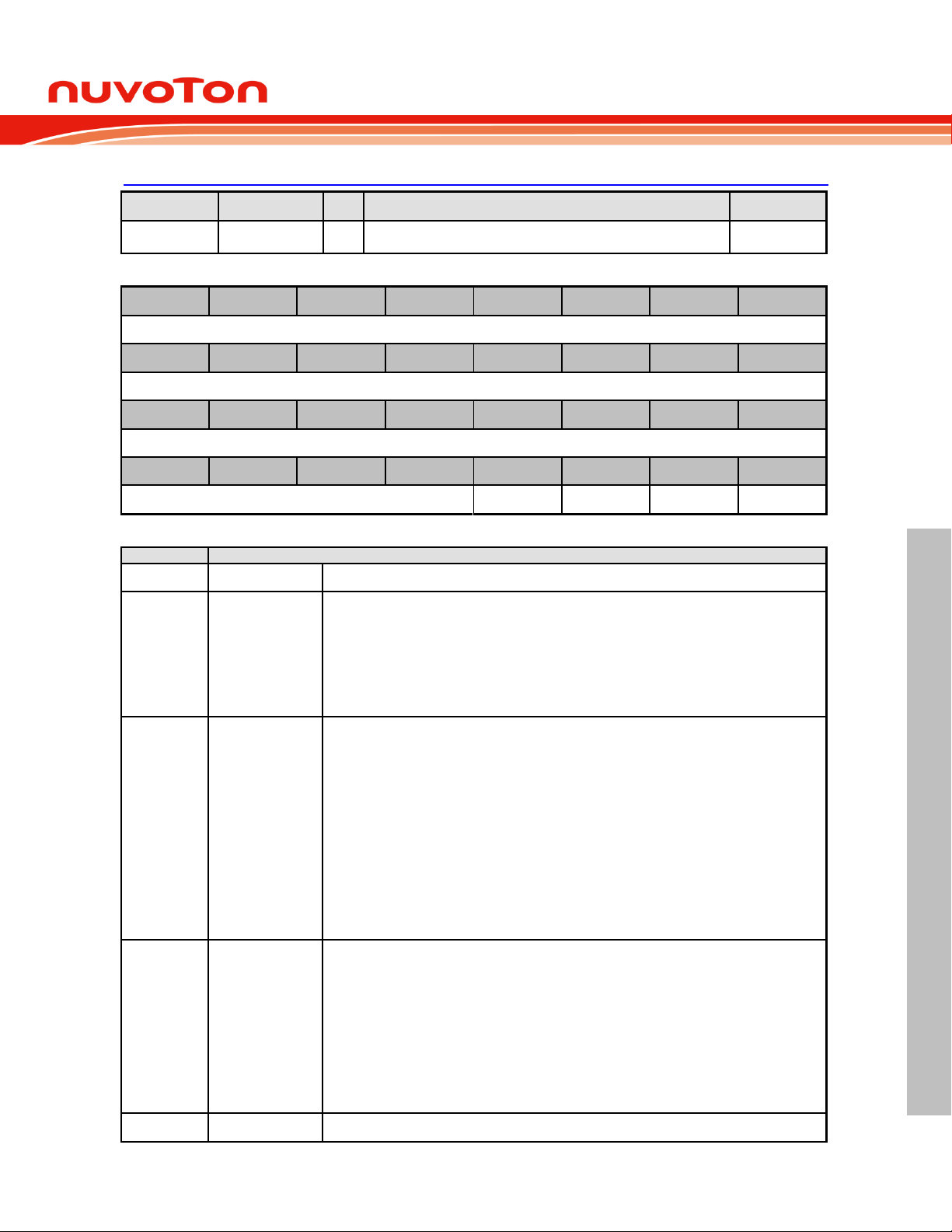
NuMicro® NUC029LEE/NUC029SEE
NUMICRO
®
NUC029LEE/NUC029SEE TECHNICAL REFERENCE MANUAL
Register
Offset
R/W
Description
Reset Value
HIRCTSTS
GCR_BA+0x98
R/W
HIRC Trim Interrupt Status Register
0x0000_0000
31
30
29
28
27
26
25
24
Reserved
23
22
21
20
19
18
17
16
Reserved
15
14
13
12
11
10 9 8
Reserved
7 6 5 4 3 2 1
0
Reserved
OVBDIF
CLKERIF
TFAILIF
FREQLOCK
Bits
Description
[31:4]
Reserved
Reserved.
[3]
OVBDIF
Over Boundary Status
When the over boundary function is set, if there occurs the over boundary condition, this
flag will be set.
0 = Over boundary coundition did not occur.
1 = Over boundary coundition occurred.
Note: Write 1 to clear this flag.
[2]
CLKERIF
Clock Error Interrupt Status
When the reference clock or 48MHz internal high speed RC oscillator (HIRC) is shift larger
to unreasonable value, this bit will be set and to be an indicate that clock frequency is
inaccuracy
Once this bit is set to 1, the auto trim operation stopped and
FREQSEL(SYS_HIRCTCTL[1:0]) will be cleared to 00 by hardware automatically if
CESTOPEN(SYS_HIRCTCTL[8]) is set to 1.
If this bit is set and CLKEIEN(SYS_HIRCTIEN[2]) is high, an interrupt will be triggered to
notify the clock frequency is inaccuracy. Write 1 to clear this to 0.
0 = Clock frequency is accuracy.
1 = Clock frequency is inaccuracy.
Note : reset by powr on reset
[1]
TFAILIF
Trim Failure Interrupt Status
This bit indicates that HIRC trim value update limitation count reached and the HIRC clock
frequency still doesn’t be locked. Once this bit is set, the auto trim operation stopped and
FREQSEL(SYS_HIRCTCTL[1:0]) will be cleared to 00 by hardware automatically.
If this bit is set and TFAILIEN(SYS_HIRCTIEN[1]) is high, an interrupt will be triggered to
notify that HIRC trim value update limitation count was reached. Write 1 to clear this to 0.
0 = Trim value update limitation count does not reach.
1 = Trim value update limitation count reached and HIRC frequency still not locked.
Note : reset by powr on reset
[0]
FREQLOCK
HIRC Frequency Lock Status
32-bit Arm® Cortex®-M0 Microcontroller
HIRC Trim Interrupt Status Register (SYS_HIRCTSTS)
Aug, 2018 Page 71 of 497 Rev 1.00
Page 72
NUMICRO
®
NUC029LEE/NUC029SEE TECHNICAL REFERENCE MANUAL
This bit indicates the HIRC frequency is locked.
This is a status bit and doesn’t trigger any interrupt
Write 1 to clear this to 0. This bit will be set automatically, if the frequecy is lock and the
RC_TRIM is enabled.
0 = The internal high-speed oscillator frequency doesn’t lock at 48 MHz yet.
1 = The internal high-speed oscillator frequency locked at 48 MHz.
Note : reset by powr on reset
NuMicro® NUC029LEE/NUC029SEE
32-bit Arm® Cortex®-M0 Microcontroller
Aug, 2018 Page 72 of 497 Rev 1.00
Page 73
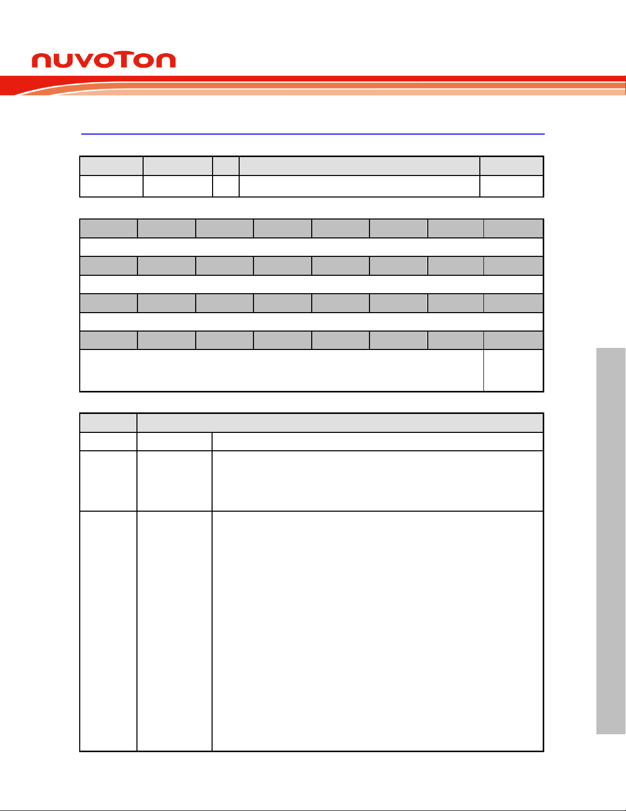
NuMicro® NUC029LEE/NUC029SEE
NUMICRO
®
NUC029LEE/NUC029SEE TECHNICAL REFERENCE MANUAL
Register
Offset
R/W
Description
Reset Value
REGWRPROT
GCR_BA+0x100
R/W
Register Write Protection Register
0x0000_0000
31
30
29
28
27
26
25
24
Reserved
23
22
21
20
19
18
17
16
Reserved
15
14
13
12
11
10 9 8
Reserved
7 6 5 4 3 2 1
0
REGWRPROT[7:1]
REGWRPROT
[0]
REGPROTDIS
Bits
Description
[31:16]
Reserved
Reserved.
[7:0]
REGWRPROT
Register Write-Protection Code (Write Only)
Some registers have write-protection function. Writing these registers have to disable the
protected function by writing the sequence value “59h”, “16h”, “88h” to this field. After this
sequence is completed, the REGPROTDIS bit will be set to 1 and write-protection
registers can be normal write.
[0]
REGPROTDIS
Register Write-Protection Disable Index (Read Only)
0 = Write-protection is enabled for writing protected registers. Any write to the protected
register is ignored.
1 = Write-protection is disabled for writing protected registers.
The Protected registers are:
IPRSTC1: address 0x5000_0008
BODCR: address 0x5000_0018
PORCR: address 0x5000_0024
PWRCON: address 0x5000_0200 (bit[6] is not protected for power wake-up interrupt clear)
APBCLK bit[0]: address 0x5000_0208 (bit[0] is Watchdog Timer clock enable)
CLKSEL0: address 0x5000_0210 (for HCLK and CPU STCLK clock source selection)
CLKSEL1 bit[1:0]: address 0x5000_0214 (for Watchdog Timer clock source selection)
NMI_SEL bit[8]: address 0x5000_0380 (for NMI_EN interrupt enable)
ISPCON: address 0x5000_C000 (Flash ISP Control register)
ISPTRG: address 0x5000_C010 (ISP Trigger Control register)
WTCR: address 0x4000_4000
FATCON: address 0x5000_C018
Note: The bits which are write-protected will be noted as” (Write Protect)” beside the
32-bit Arm® Cortex®-M0 Microcontroller
Register Write Protection Register (REGWRPROT)
This register is write for disable/enable register protection and read for the REGPROTDIS status
Aug, 2018 Page 73 of 497 Rev 1.00
Page 74

NuMicro® NUC029LEE/NUC029SEE
NUMICRO
®
NUC029LEE/NUC029SEE TECHNICAL REFERENCE MANUAL
description.
32-bit Arm® Cortex®-M0 Microcontroller
6.2.9 System Timer (SysTick)
The Cortex®-M0 includes an integrated system timer, SysTick, which provides a simple, 24-bit
clear-on-write, decrementing, wrap-on-zero counter with a flexible control mechanism. The
counter can be used as a Real Time Operating System (RTOS) tick timer or as a simple counter.
When system timer is enabled, it will count down from the value in the SysTick Current Value
Register (SYST_CVR) to 0, and reload (wrap) to the value in the SysTick Reload Value Register
(SYST_RVR) on the next clock cycle, then decrement on subsequent clocks. When the counter
transitions to 0, the COUNTFLAG status bit is set. The COUNTFLAG bit clears on reads.
The SYST_CVR value is UNKNOWN on reset. Software should write to the register to clear it to 0
before enabling the feature. This ensures the timer will count from the SYST_RVR value rather
than an arbitrary value when it is enabled.
If the SYST_RVR is 0, the timer will be maintained with a current value of 0 after it is reloaded
with this value. This mechanism can be used to disable the feature independently from the timer
enable bit.
For more detailed information, please refer to the “ARM® Cortex®-M0 Technical Reference
Manual” and “ARM
®
v6-M Architecture Reference Manual”.
Aug, 2018 Page 74 of 497 Rev 1.00
Page 75
NUMICRO
®
NUC029LEE/NUC029SEE TECHNICAL REFERENCE MANUAL
6.2.9.1 System Timer Control Register Map
Register
Offset
R/W
Description
Reset Value
SYST Base Address:
SCS_BA = 0xE000_E000
SYST_CSR
SCS_BA+0x10
R/W
SysTick Control and Status Register
0x0000_0000
SYST_RVR
SCS_BA+0x14
R/W
SysTick Reload Value Register
0xXXXX_XXXX
SYST_CVR
SCS_BA+0x18
R/W
SysTick Current Value Register
0xXXXX_XXXX
R: read only, W: write only, R/W: both read and write
NuMicro® NUC029LEE/NUC029SEE
32-bit Arm® Cortex®-M0 Microcontroller
Aug, 2018 Page 75 of 497 Rev 1.00
Page 76
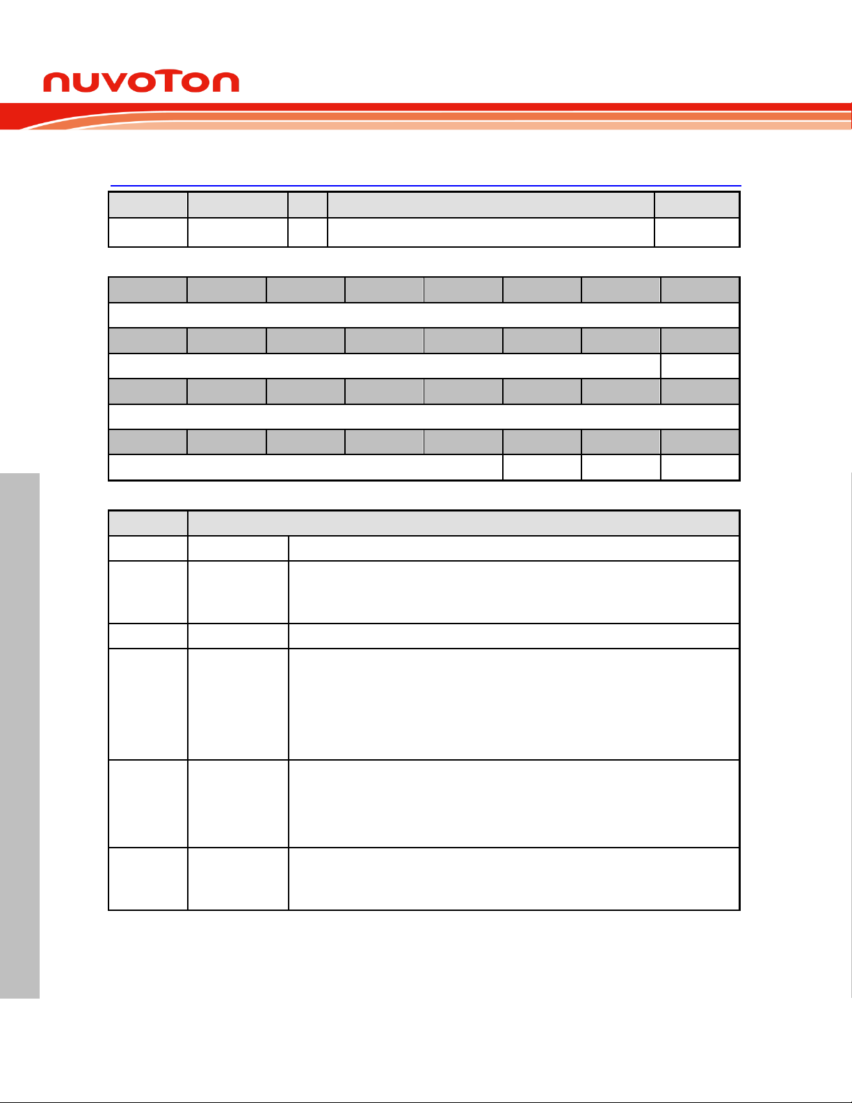
NuMicro® NUC029LEE/NUC029SEE
NUMICRO
®
NUC029LEE/NUC029SEE TECHNICAL REFERENCE MANUAL
Register
Offset
R/W
Description
Reset Value
SYST_CSR
SCS_BA+0x10
R/W
SysTick Control and Status Register
0x0000_0000
31
30
29
28
27
26
25
24
Reserved
23
22
21
20
19
18
17
16
Reserved
COUNTFLAG
15
14
13
12
11
10 9 8
Reserved
7 6 5 4 3 2 1
0
Reserved
CLKSRC
TICKINT
ENABLE
Bits
Description
[31:17]
Reserved
Reserved.
[16]
COUNTFLAG
Returns 1 If Timer Counted To 0 Since Last Time This Register Was Read
COUNTFLAG is set by a count transition from 1 to 0.
COUNTFLAG is cleared on read or by a write to the Current Value register.
[15:3]
Reserved
Reserved.
[2]
CLKSRC
System Tick Clock Source Selection
If CLKSRC(SYST_CSR[2]) = 1, SysTick clock source is from HCLK.
If CLKSRC(SYST_CSR[2]) = 0, SysTick clock source is defined by
STCLK_S(CLKSEL0[5:3]).
0 = Clock source is (optional) external reference clock.
1 = Core clock used for SysTick.
[1]
TICKINT
System Tick Interrupt Enabled
0 = Counting down to 0 does not cause the SysTick exception to be pended. Software can
use COUNTFLAG to determine if a count to 0 has occurred.
1 = Counting down to 0 will cause the SysTick exception to be pended. Clearing the
SysTick Current Value register by a write in software will not cause SysTick to be pended.
[0]
ENABLE
System Tick Counter Enabled
0 = Counter Disabled.
1 = Counter will operate in a multi-shot manner.
32-bit Arm® Cortex®-M0 Microcontroller
6.2.9.2 System Timer Control Register Description
SysTick Control and Status (SYST_CSR)
Aug, 2018 Page 76 of 497 Rev 1.00
Page 77
NuMicro® NUC029LEE/NUC029SEE
NUMICRO
®
NUC029LEE/NUC029SEE TECHNICAL REFERENCE MANUAL
Register
Offset
R/W
Description
Reset Value
SYST_RVR
SCS_BA+0x14
R/W
SysTick Reload Value Register
0xXXXX_XXXX
31
30
29
28
27
26
25
24
Reserved
23
22
21
20
19
18
17
16
RELOAD
15
14
13
12
11
10 9 8
RELOAD
7 6 5 4 3 2 1
0
RELOAD
Bits
Description
[31:24]
Reserved
Reserved.
[23:0]
RELOAD
Value to load into the Current Value register when the counter reaches 0.
32-bit Arm® Cortex®-M0 Microcontroller
SysTick Reload Value Register (SYST_RVR)
Aug, 2018 Page 77 of 497 Rev 1.00
Page 78
NuMicro® NUC029LEE/NUC029SEE
NUMICRO
®
NUC029LEE/NUC029SEE TECHNICAL REFERENCE MANUAL
Register
Offset
R/W
Description
Reset Value
SYST_CVR
SCS_BA+0x18
R/W
SysTick Current Value Register
0xXXXX_XXXX
31
30
29
28
27
26
25
24
Reserved
23
22
21
20
19
18
17
16
CURRENT
15
14
13
12
11
10 9 8
CURRENT
7 6 5 4 3 2 1
0
CURRENT
Bits
Description
[31:24]
Reserved
Reserved.
[23:0]
CURRENT
System Tick Current Value
Current counter value. This is the value of the counter at the time it is sampled. The
counter does not provide read-modify-write protection. The register is write-clear. A
software write of any value will clear the register to 0.
32-bit Arm® Cortex®-M0 Microcontroller
SysTick Current Value Register (SYST_CVR)
Aug, 2018 Page 78 of 497 Rev 1.00
Page 79

NuMicro® NUC029LEE/NUC029SEE
NUMICRO
®
NUC029LEE/NUC029SEE TECHNICAL REFERENCE MANUAL
32-bit Arm® Cortex®-M0 Microcontroller
6.2.10 Nested Vectored Interrupt Controller (NVIC)
The Cortex®-M0 provides an interrupt controller as an integral part of the exception mode, named
as “Nested Vectored Interrupt Controller (NVIC)”, which is closely coupled to the processor kernel
and provides following features:
Nested and Vectored interrupt support
Automatic processor state saving and restoration
Reduced and deterministic interrupt latency
The NVIC prioritizes and handles all supported exceptions. All exceptions are handled in “Handler
Mode”. This NVIC architecture supports 32 (IRQ[31:0]) discrete interrupts with 4 levels of priority.
All of the interrupts and most of the system exceptions can be configured to different priority
levels. When an interrupt occurs, the NVIC will compare the priority of the new interrupt to the
current running one’s priority. If the priority of the new interrupt is higher than the current one, the
new interrupt handler will override the current handler.
When an interrupt is accepted, the starting address of the interrupt service routine (ISR) is fetched
from a vector table in memory. There is no need to determine which interrupt is accepted and
branch to the starting address of the correlated ISR by software. While the starting address is
fetched, NVIC will also automatically save processor state including the registers “PC, PSR, LR,
R0~R3, R12” to the stack. At the end of the ISR, the NVIC will restore the mentioned registers
from stack and resume the normal execution. Thus it will take less and deterministic time to
process the interrupt request.
The NVIC supports “Tail Chaining” which handles back-to-back interrupts efficiently without the
overhead of states saving and restoration and therefore reduces delay time in switching to
pending ISR at the end of current ISR. The NVIC also supports “Late Arrival” which improves the
efficiency of concurrent ISRs. When a higher priority interrupt request occurs before the current
ISR starts to execute (at the stage of state saving and starting address fetching), the NVIC will
give priority to the higher one without delay penalty. Thus it advances the real-time capability.
For more detailed information, please refer to the “ARM
Manual” and “ARM
®
v6-M Architecture Reference Manual”.
®
Cortex®-M0 Technical Reference
Aug, 2018 Page 79 of 497 Rev 1.00
Page 80
NuMicro® NUC029LEE/NUC029SEE
NUMICRO
®
NUC029LEE/NUC029SEE TECHNICAL REFERENCE MANUAL
Exception Name
Vector Number
Priority
Reset
1
-3
NMI
2
-2
Hard Fault
3
-1
Reserved
4 ~ 10
Reserved
SVCall
11
Configurable
Reserved
12 ~ 13
Reserved
PendSV
14
Configurable
SysTick
15
Configurable
Interrupt (IRQ0 ~ IRQ31)
16 ~ 47
Configurable
Vector
Number
Interrupt Number
(Bit In Interrupt
Registers)
Interrupt Name
Source
Module
Interrupt Description
1 ~ 15
- - -
System exceptions
16
0
BOD_INT
Brown-out
Brown-out low voltage detected interrupt
17
1
WDT_INT
WDT
Watchdog Timer interrupt
18
2
EINT0
GPIO
External signal interrupt from PB.14 pin
19
3
EINT1
GPIO
External signal interrupt from PB.15 pin
20
4
GPAB_INT
GPIO
External signal interrupt from
PA[6:0]/PA[15:8]/PB[11:0]/PB[15:13]
21
5
GPCEF_INT
GPIO
External interrupt from
PC[3:0]/PC[11:6]/PC[15:14]/PE[5]/PF[1:0]
22
6
PWMA_INT
PWM0~3
PWM0, PWM1, PWM2 and PWM3 interrupt
23
7
PWMB_INT
PWM4~7
PWM4 and PWM5 interrupt
24
8
TMR0_INT
TMR0
Timer 0 interrupt
25
9
TMR1_INT
TMR1
Timer 1 interrupt
26
10
TMR2_INT
TMR2
Timer 2 interrupt
27
11
TMR3_INT
TMR3
Timer 3 interrupt
28
12
UART02_INT
UART0/2
UART0 and UART2 interrupt
32-bit Arm® Cortex®-M0 Microcontroller
6.2.10.1 Exception Model and System Interrupt Map
The following table lists the exception model supported by NuMicro® NUC029LEE/NUC029SEE.
Software can set four levels of priority on some of these exceptions as well as on all interrupts.
The highest user-configurable priority is denoted as “0” and the lowest priority is denoted as “3”.
The default priority of all the user-configurable interrupts is “0”. Note that priority “0” is treated as
the fourth priority on the system, after three system exceptions “Reset”, “NMI” and “Hard Fault”.
Table 6.2-2 Exception Model
Aug, 2018 Page 80 of 497 Rev 1.00
Page 81
NuMicro® NUC029LEE/NUC029SEE
NUMICRO
®
NUC029LEE/NUC029SEE TECHNICAL REFERENCE MANUAL
29
13
UART1_INT
UART1
UART1 interrupt
30
14
SPI0_INT
SPI0
SPI0 interrupt
31
15
SPI1_INT
SPI1
SPI1 interrupt
32
16 - -
Reserved
33
17 - -
Reserved
34
18
I2C0_INT
I2C0
I2C0 interrupt
35
19
I2C1_INT
I2C1
I2C1 interrupt
36
20 - -
Reserved
37
21 - -
Reserved
38
22 - -
Reserved
39
23
USB_INT
USBD
USB 2.0 FS Device interrupt
40
24 - -
Reserved
41
25 - -
Reserved
42
26
PDMA_INT
PDMA
PDMA interrupt
43
27 - -
Reserved
44
28
PWRWU_INT
CLKC
Clock controller interrupt for chip wake-up from Powerdown state
45
29
ADC_INT
ADC
ADC interrupt
46
30
IRC_INT
IRC
IRC TRIM interrupt
47
31
RTC_INT
RTC
Real Time Clock interrupt
Vector Table Word Offset
Description
0
SP_main – The Main stack pointer
Vector Number
Exception Entry Pointer using that Vector Number
32-bit Arm® Cortex®-M0 Microcontroller
Table 6.2-3 System Interrupt Map
6.2.10.2 Vector Table
When an interrupt is accepted, the processor will automatically fetch the starting address of the
interrupt service routine (ISR) from a vector table in memory. For ARMv6-M, the vector table base
address is fixed at 0x00000000. The vector table contains the initialization value for the stack
pointer on reset, and the entry point addresses for all exception handlers. The vector number on
previous page defines the order of entries in the vector table associated with exception handler
entry as illustrated in previous section.
Table 6.2-4 Vector Table Format
6.2.10.3 Operation Description
NVIC interrupts can be enabled and disabled by writing to their corresponding Interrupt Set-
Aug, 2018 Page 81 of 497 Rev 1.00
Page 82

NuMicro® NUC029LEE/NUC029SEE
NUMICRO
®
NUC029LEE/NUC029SEE TECHNICAL REFERENCE MANUAL
32-bit Arm® Cortex®-M0 Microcontroller
Enable or Interrupt Clear-Enable register bit-field. The registers use a write-1-to-enable and write1-to-clear policy, both registers reading back the current enabled state of the corresponding
interrupts. When an interrupt is disabled, interrupt assertion will cause the interrupt to become
Pending, however, the interrupt will not activate. If an interrupt is Active when it is disabled, it
remains in its Active state until cleared by reset or an exception return. Clearing the enable bit
prevents new activations of the associated interrupt.
NVIC interrupts can be pended/un-pended using a complementary pair of registers to those used
to enable/disable the interrupts, named the Set-Pending Register and Clear-Pending Register
respectively. The registers use a write-1-to-enable and write-1-to-clear policy, both registers
reading back the current pended state of the corresponding interrupts. The Clear-Pending
Register has no effect on the execution status of an Active interrupt.
NVIC interrupts are prioritized by updating an 8-bit field within a 32-bit register (each register
supporting four interrupts).
The general registers associated with the NVIC are all accessible from a block of memory in the
System Control Space and will be described in next section.
Aug, 2018 Page 82 of 497 Rev 1.00
Page 83
NUMICRO
®
NUC029LEE/NUC029SEE TECHNICAL REFERENCE MANUAL
6.2.10.4 NVIC Control Register Map
Register
Offset
R/W
Description
Reset Value
NVIC Base Address:
SCS_BA = 0xE000_E000
NVIC_ISER
SCS_BA+0x100
R/W
IRQ0 ~ IRQ31 Set-enable Control Register
0x0000_0000
NVIC_ICER
SCS_BA+0x180
R/W
IRQ0 ~ IRQ31 Clear-enable Control Register
0x0000_0000
NVIC_ISPR
SCS_BA+0x200
R/W
IRQ0 ~ IRQ31 Set-pending Control Register
0x0000_0000
NVIC_ICPR
SCS_BA+0x280
R/W
IRQ0 ~ IRQ31 Clear-pending Control Register
0x0000_0000
NVIC_IPR0
SCS_BA+0x400
R/W
IRQ0 ~ IRQ3 Priority Control Register
0x0000_0000
NVIC_IPR1
SCS_BA+0x404
R/W
IRQ4 ~ IRQ7 Priority Control Register
0x0000_0000
NVIC_IPR2
SCS_BA+0x408
R/W
IRQ8 ~ IRQ11 Priority Control Register
0x0000_0000
NVIC_IPR3
SCS_BA+0x40C
R/W
IRQ12 ~ IRQ15 Priority Control Register
0x0000_0000
NVIC_IPR4
SCS_BA+0x410
R/W
IRQ16 ~ IRQ19 Priority Control Register
0x0000_0000
NVIC_IPR5
SCS_BA+0x414
R/W
IRQ20 ~ IRQ23 Priority Control Register
0x0000_0000
NVIC_IPR6
SCS_BA+0x418
R/W
IRQ24 ~ IRQ27 Priority Control Register
0x0000_0000
NVIC_IPR7
SCS_BA+0x41C
R/W
IRQ28 ~ IRQ31 Priority Control Register
0x0000_0000
R: read only, W: write only, R/W: both read and write
NuMicro® NUC029LEE/NUC029SEE
32-bit Arm® Cortex®-M0 Microcontroller
Aug, 2018 Page 83 of 497 Rev 1.00
Page 84
NuMicro® NUC029LEE/NUC029SEE
NUMICRO
®
NUC029LEE/NUC029SEE TECHNICAL REFERENCE MANUAL
Register
Offset
R/W
Description
Reset Value
NVIC_ISER
SCS_BA+0x100
R/W
IRQ0 ~ IRQ31 Set-enable Control Register
0x0000_0000
31
30
29
28
27
26
25
24
SETENA
23
22
21
20
19
18
17
16
SETENA
15
14
13
12
11
10 9 8
SETENA
7 6 5 4 3 2 1
0
SETENA
Bits
Description
[31:0]
SETENA
Interrupt Enable Register
Enable one or more interrupts. Each bit represents an interrupt number from IRQ0 ~
IRQ31 (Vector number from 16 ~ 47).
Write Operation:
0 = No effect.
1 = Write 1 to enable associated interrupt.
Read Operation:
0 = Associated interrupt status is Disabled.
1 = Associated interrupt status is Enabled.
Read value indicates the current enable status.
32-bit Arm® Cortex®-M0 Microcontroller
6.2.10.5 NVIC Control Register Description
IRQ0 ~ IRQ31 Set-Enable Control Register (NVIC_ISER)
Aug, 2018 Page 84 of 497 Rev 1.00
Page 85
NuMicro® NUC029LEE/NUC029SEE
NUMICRO
®
NUC029LEE/NUC029SEE TECHNICAL REFERENCE MANUAL
Register
Offset
R/W
Description
Reset Value
NVIC_ICER
SCS_BA+0x180
R/W
IRQ0 ~ IRQ31 Clear-enable Control Register
0x0000_0000
31
30
29
28
27
26
25
24
CLRENA
23
22
21
20
19
18
17
16
CLRENA
15
14
13
12
11
10 9 8
CLRENA
7 6 5 4 3 2 1
0
CLRENA
Bits
Description
[31:0]
CLRENA
Interrupt Disable Bits
Disable one or more interrupts. Each bit represents an interrupt number from IRQ0 ~
IRQ31 (Vector number from 16 ~ 47).
Write Operation:
0 = No effect.
1 = Write 1 to disable associated interrupt.
Read Operation:
0 = Associated interrupt status is Disabled.
1 = Associated interrupt status is Enabled.
Read value indicates the current enable status.
32-bit Arm® Cortex®-M0 Microcontroller
IRQ0 ~ IRQ31 Clear-Enable Control Register (NVIC_ICER)
Aug, 2018 Page 85 of 497 Rev 1.00
Page 86
NuMicro® NUC029LEE/NUC029SEE
NUMICRO
®
NUC029LEE/NUC029SEE TECHNICAL REFERENCE MANUAL
Register
Offset
R/W
Description
Reset Value
NVIC_ISPR
SCS_BA+0x200
R/W
IRQ0 ~ IRQ31 Set-pending Control Register
0x0000_0000
31
30
29
28
27
26
25
24
SETPEND
23
22
21
20
19
18
17
16
SETPEND
15
14
13
12
11
10 9 8
SETPEND
7 6 5 4 3 2 1
0
SETPEND
Bits
Description
[31:0]
SETPEND
Set Interrupt Pending Register
Write Operation:
0 = No effect.
1 = Write 1 to set pending state. Each bit represents an interrupt number from IRQ0 ~
IRQ31 (Vector number from 16 ~ 47).
Read Operation:
0 = Associated interrupt in not in pending status.
1 = Associated interrupt is in pending status.
Read value indicates the current pending status.
32-bit Arm® Cortex®-M0 Microcontroller
IRQ0 ~ IRQ31 Set-Pending Control Register (NVIC_ISPR)
Aug, 2018 Page 86 of 497 Rev 1.00
Page 87
NuMicro® NUC029LEE/NUC029SEE
NUMICRO
®
NUC029LEE/NUC029SEE TECHNICAL REFERENCE MANUAL
Register
Offset
R/W
Description
Reset Value
NVIC_ICPR
SCS_BA+0x280
R/W
IRQ0 ~ IRQ31 Clear-Pending Control Register
0x0000_0000
31
30
29
28
27
26
25
24
CLRPEND
23
22
21
20
19
18
17
16
CLRPEND
15
14
13
12
11
10 9 8
CLRPEND
7 6 5 4 3 2 1
0
CLRPEND
Bits
Description
[31:0]
CLRPEND
Clear Interrupt Pending Register
Write Operation:
0 = No effect.
1 = Write 1 to clear pending state. Each bit represents an interrupt number from IRQ0 ~
IRQ31 (Vector number from 16 ~ 47).
Read Operation:
0 = Associated interrupt in not in pending status.
1 = Associated interrupt is in pending status.
Read value indicates the current pending status.
32-bit Arm® Cortex®-M0 Microcontroller
IRQ0 ~ IRQ31 Clear-Pending Control Register (NVIC_ICPR)
Aug, 2018 Page 87 of 497 Rev 1.00
Page 88
NuMicro® NUC029LEE/NUC029SEE
NUMICRO
®
NUC029LEE/NUC029SEE TECHNICAL REFERENCE MANUAL
Register
Offset
R/W
Description
Reset Value
NVIC_IPR0
SCS_BA+0x400
R/W
IRQ0 ~ IRQ3 Priority Control Register
0x0000_0000
31
30
29
28
27
26
25
24
PRI_3
Reserved
23
22
21
20
19
18
17
16
PRI_2
Reserved
15
14
13
12
11
10 9 8
PRI_1
Reserved
7 6 5 4 3 2 1
0
PRI_0
Reserved
Bits
Description
[31:30]
PRI_3
Priority Of IRQ3
“0” denotes the highest priority and “3” denotes the lowest priority.
[29:24]
Reserved
Reserved.
[23:22]
PRI_2
Priority Of IRQ2
“0” denotes the highest priority and “3” denotes the lowest priority.
[21:16]
Reserved
Reserved.
[15:14]
PRI_1
Priority Of IRQ1
“0” denotes the highest priority and “3” denotes the lowest priority.
[13:8]
Reserved
Reserved.
[7:6]
PRI_0
Priority Of IRQ0
“0” denotes the highest priority and “3” denotes the lowest priority.
[5:0]
Reserved
Reserved.
32-bit Arm® Cortex®-M0 Microcontroller
IRQ0 ~ IRQ3 Priority Register (NVIC_IPR0)
Aug, 2018 Page 88 of 497 Rev 1.00
Page 89
NuMicro® NUC029LEE/NUC029SEE
NUMICRO
®
NUC029LEE/NUC029SEE TECHNICAL REFERENCE MANUAL
Register
Offset
R/W
Description
Reset Value
NVIC_IPR1
SCS_BA+0x404
R/W
IRQ4 ~ IRQ7 Priority Control Register
0x0000_0000
31
30
29
28
27
26
25
24
PRI_7
Reserved
23
22
21
20
19
18
17
16
PRI_6
Reserved
15
14
13
12
11
10 9 8
PRI_5
Reserved
7 6 5 4 3 2 1
0
PRI_4
Reserved
Bits
Description
[31:30]
PRI_7
Priority Of IRQ7
“0” denotes the highest priority and “3” denotes the lowest priority.
[29:24]
Reserved
Reserved.
[23:22]
PRI_6
Priority Of IRQ6
“0” denotes the highest priority and “3” denotes the lowest priority.
[21:16]
Reserved
Reserved.
[15:14]
PRI_5
Priority Of IRQ5
“0” denotes the highest priority and “3” denotes the lowest priority.
[13:8]
Reserved
Reserved.
[7:6]
PRI_4
Priority Of IRQ4
“0” denotes the highest priority and “3” denotes the lowest priority.
[5:0]
Reserved
Reserved.
32-bit Arm® Cortex®-M0 Microcontroller
IRQ4 ~ IRQ7 Priority Register (NVIC_IPR1)
Aug, 2018 Page 89 of 497 Rev 1.00
Page 90
NuMicro® NUC029LEE/NUC029SEE
NUMICRO
®
NUC029LEE/NUC029SEE TECHNICAL REFERENCE MANUAL
Register
Offset
R/W
Description
Reset Value
NVIC_IPR2
SCS_BA+0x408
R/W
IRQ8 ~ IRQ11 Priority Control Register
0x0000_0000
31
30
29
28
27
26
25
24
PRI_11
Reserved
23
22
21
20
19
18
17
16
PRI_10
Reserved
15
14
13
12
11
10 9 8
PRI_9
Reserved
7 6 5 4 3 2 1
0
PRI_8
Reserved
Bits
Description
[31:30]
PRI_11
Priority Of IRQ11
“0” denotes the highest priority and “3” denotes the lowest priority.
[29:24]
Reserved
Reserved.
[23:22]
PRI_10
Priority Of IRQ10
“0” denotes the highest priority and “3” denotes the lowest priority.
[21:16]
Reserved
Reserved.
[15:14]
PRI_9
Priority Of IRQ9
“0” denotes the highest priority and “3” denotes the lowest priority.
[13:8]
Reserved
Reserved.
[7:6]
PRI_8
Priority Of IRQ8
“0” denotes the highest priority and “3” denotes the lowest priority.
[5:0]
Reserved
Reserved.
32-bit Arm® Cortex®-M0 Microcontroller
IRQ8 ~ IRQ11 Priority Register (NVIC_IPR2)
Aug, 2018 Page 90 of 497 Rev 1.00
Page 91
NuMicro® NUC029LEE/NUC029SEE
NUMICRO
®
NUC029LEE/NUC029SEE TECHNICAL REFERENCE MANUAL
Register
Offset
R/W
Description
Reset Value
NVIC_IPR3
SCS_BA+0x40C
R/W
IRQ12 ~ IRQ15 Priority Control Register
0x0000_0000
31
30
29
28
27
26
25
24
PRI_15
Reserved
23
22
21
20
19
18
17
16
PRI_14
Reserved
15
14
13
12
11
10 9 8
PRI_13
Reserved
7 6 5 4 3 2 1
0
PRI_12
Reserved
Bits
Description
[31:30]
PRI_15
Priority Of IRQ15
“0” denotes the highest priority and “3” denotes the lowest priority.
[29:24]
Reserved
Reserved.
[23:22]
PRI_14
Priority Of IRQ14
“0” denotes the highest priority and “3” denotes the lowest priority.
[21:16]
Reserved
Reserved.
[15:14]
PRI_13
Priority Of IRQ13
“0” denotes the highest priority and “3” denotes the lowest priority
[13:8]
Reserved
Reserved.
[7:6]
PRI_12
Priority Of IRQ12
“0” denotes the highest priority and “3” denotes the lowest priority.
[5:0]
Reserved
Reserved.
32-bit Arm® Cortex®-M0 Microcontroller
IRQ12 ~ IRQ15 Priority Register (NVIC_IPR3)
Aug, 2018 Page 91 of 497 Rev 1.00
Page 92
NuMicro® NUC029LEE/NUC029SEE
NUMICRO
®
NUC029LEE/NUC029SEE TECHNICAL REFERENCE MANUAL
Register
Offset
R/W
Description
Reset Value
NVIC_IPR4
SCS_BA+0x410
R/W
IRQ16 ~ IRQ19 Priority Control Register
0x0000_0000
31
30
29
28
27
26
25
24
PRI_19
Reserved
23
22
21
20
19
18
17
16
PRI_18
Reserved
15
14
13
12
11
10 9 8
PRI_17
Reserved
7 6 5 4 3 2 1
0
PRI_16
Reserved
Bits
Description
[31:30]
PRI_19
Priority Of IRQ19
“0” denotes the highest priority and “3” denotes the lowest priority.
[29:24]
Reserved
Reserved.
[23:22]
PRI_18
Priority Of IRQ18
“0” denotes the highest priority and “3” denotes the lowest priority.
[21:16]
Reserved
Reserved.
[15:14]
PRI_17
Priority Of IRQ17
“0” denotes the highest priority and “3” denotes the lowest priority.
[13:8]
Reserved
Reserved.
[7:6]
PRI_16
Priority Of IRQ16
“0” denotes the highest priority and “3” denotes the lowest priority.
[5:0]
Reserved
Reserved.
32-bit Arm® Cortex®-M0 Microcontroller
IRQ16 ~ IRQ19 Priority Register (NVIC_IPR4)
Aug, 2018 Page 92 of 497 Rev 1.00
Page 93
NuMicro® NUC029LEE/NUC029SEE
NUMICRO
®
NUC029LEE/NUC029SEE TECHNICAL REFERENCE MANUAL
Register
Offset
R/W
Description
Reset Value
NVIC_IPR5
SCS_BA+0x414
R/W
IRQ20 ~ IRQ23 Priority Control Register
0x0000_0000
31
30
29
28
27
26
25
24
PRI_23
Reserved
23
22
21
20
19
18
17
16
PRI_22
Reserved
15
14
13
12
11
10 9 8
PRI_21
Reserved
7 6 5 4 3 2 1
0
PRI_20
Reserved
Bits
Description
[31:30]
PRI_23
Priority Of IRQ23
“0” denotes the highest priority and “3” denotes the lowest priority.
[29:24]
Reserved
Reserved.
[23:22]
PRI_22
Priority Of IRQ22
“0” denotes the highest priority and “3” denotes the lowest priority.
[21:16]
Reserved
Reserved.
[15:14]
PRI_21
Priority Of IRQ21
“0” denotes the highest priority and “3” denotes the lowest priority
[13:8]
Reserved
Reserved.
[7:6]
PRI_20
Priority Of IRQ20
“0” denotes the highest priority and “3” denotes the lowest priority.
[5:0]
Reserved
Reserved.
32-bit Arm® Cortex®-M0 Microcontroller
IRQ20 ~ IRQ23 Priority Register (NVIC_IPR5)
Aug, 2018 Page 93 of 497 Rev 1.00
Page 94
NuMicro® NUC029LEE/NUC029SEE
NUMICRO
®
NUC029LEE/NUC029SEE TECHNICAL REFERENCE MANUAL
Register
Offset
R/W
Description
Reset Value
NVIC_IPR6
SCS_BA+0x418
R/W
IRQ24 ~ IRQ27 Priority Control Register
0x0000_0000
31
30
29
28
27
26
25
24
PRI_27
Reserved
23
22
21
20
19
18
17
16
PRI_26
Reserved
15
14
13
12
11
10 9 8
PRI_25
Reserved
7 6 5 4 3 2 1
0
PRI_24
Reserved
Bits
Description
[31:30]
PRI_27
Priority Of IRQ27
“0” denotes the highest priority and “3” denotes the lowest priority.
[29:24]
Reserved
Reserved.
[23:22]
PRI_26
Priority Of IRQ26
“0” denotes the highest priority and “3” denotes the lowest priority.
[21:16]
Reserved
Reserved.
[15:14]
PRI_25
Priority Of IRQ25
“0” denotes the highest priority and “3” denotes the lowest priority.
[13:8]
Reserved
Reserved.
[7:6]
PRI_24
Priority Of IRQ24
“0” denotes the highest priority and “3” denotes the lowest priority.
[5:0]
Reserved
Reserved.
32-bit Arm® Cortex®-M0 Microcontroller
IRQ24 ~ IRQ27 Priority Register (NVIC_IPR6)
Aug, 2018 Page 94 of 497 Rev 1.00
Page 95
NuMicro® NUC029LEE/NUC029SEE
NUMICRO
®
NUC029LEE/NUC029SEE TECHNICAL REFERENCE MANUAL
Register
Offset
R/W
Description
Reset Value
NVIC_IPR7
SCS_BA+0x41C
R/W
IRQ28 ~ IRQ31 Priority Control Register
0x0000_0000
31
30
29
28
27
26
25
24
PRI_31
Reserved
23
22
21
20
19
18
17
16
PRI_30
Reserved
15
14
13
12
11
10 9 8
PRI_29
Reserved
7 6 5 4 3 2 1
0
PRI_28
Reserved
Bits
Description
[31:30]
PRI_31
Priority Of IRQ31
“0” denotes the highest priority and “3” denotes the lowest priority.
[29:24]
Reserved
Reserved.
[23:22]
PRI_30
Priority Of IRQ30
“0” denotes the highest priority and “3” denotes the lowest priority.
[21:16]
Reserved
Reserved.
[15:14]
PRI_29
Priority Of IRQ29
“0” denotes the highest priority and “3” denotes the lowest priority.
[13:8]
Reserved
Reserved.
[7:6]
PRI_28
Priority Of IRQ28
“0” denotes the highest priority and “3” denotes the lowest priority.
[5:0]
Reserved
Reserved.
32-bit Arm® Cortex®-M0 Microcontroller
IRQ28 ~ IRQ31 Priority Register (NVIC_IPR7)
Aug, 2018 Page 95 of 497 Rev 1.00
Page 96
NuMicro® NUC029LEE/NUC029SEE
NUMICRO
®
NUC029LEE/NUC029SEE TECHNICAL REFERENCE MANUAL
Register
Offset
R/W
Description
Reset Value
INT Base Address:
INT_BA = 0x5000_0300
IRQ0_SRC
INT_BA+0x00
R
IRQ0 (BOD) Interrupt Source Identity
0xXXXX_XXXX
IRQ1_SRC
INT_BA+0x04
R
IRQ1 (WDT) Interrupt Source Identity
0xXXXX_XXXX
IRQ2_SRC
INT_BA+0x08
R
IRQ2 (EINT0) Interrupt Source Identity
0xXXXX_XXXX
IRQ3_SRC
INT_BA+0x0C
R
IRQ3 (EINT1) Interrupt Source Identity
0xXXXX_XXXX
IRQ4_SRC
INT_BA+0x10
R
IRQ4 (GPA/B) Interrupt Source Identity
0xXXXX_XXXX
IRQ5_SRC
INT_BA+0x14
R
IRQ5 (GPC/E/F) Interrupt Source Identity
0xXXXX_XXXX
IRQ6_SRC
INT_BA+0x18
R
IRQ6 (PWMA) Interrupt Source Identity
0xXXXX_XXXX
IRQ7_SRC
INT_BA+0x1C
R
IRQ7 (PWMB) Interrupt Source Identity
0xXXXX_XXXX
IRQ8_SRC
INT_BA+0x20
R
IRQ8 (TMR0) Interrupt Source Identity
0xXXXX_XXXX
IRQ9_SRC
INT_BA+0x24
R
IRQ9 (TMR1) Interrupt Source Identity
0xXXXX_XXXX
IRQ10_SRC
INT_BA+0x28
R
IRQ10 (TMR2) Interrupt Source Identity
0xXXXX_XXXX
IRQ11_SRC
INT_BA+0x2C
R
IRQ11 (TMR3) Interrupt Source Identity
0xXXXX_XXXX
IRQ12_SRC
INT_BA+0x30
R
IRQ12 (UART0/2) Interrupt Source Identity
0xXXXX_XXXX
IRQ13_SRC
INT_BA+0x34
R
IRQ13 (UART1) Interrupt Source Identity
0xXXXX_XXXX
IRQ14_SRC
INT_BA+0x38
R
IRQ14 (SPI0) Interrupt Source Identity
0xXXXX_XXXX
IRQ15_SRC
INT_BA+0x3C
R
IRQ15 (SPI1) Interrupt Source Identity
0xXXXX_XXXX
IRQ16_SRC
INT_BA+0x40
R
Reserved
0xXXXX_XXXX
IRQ17_SRC
INT_BA+0x44
R
Reserved
0xXXXX_XXXX
IRQ18_SRC
INT_BA+0x48
R
IRQ18 (I2C0) Interrupt Source Identity
0xXXXX_XXXX
IRQ19_SRC
INT_BA+0x4C
R
IRQ19 (I2C1) Interrupt Source Identity
0xXXXX_XXXX
IRQ20_SRC
INT_BA+0x50
R
Reserved
0xXXXX_XXXX
IRQ21_SRC
INT_BA+0x54
R
Reserved
0xXXXX_XXXX
IRQ22_SRC
INT_BA+0x58
R
Reserved
0xXXXX_XXXX
32-bit Arm® Cortex®-M0 Microcontroller
6.2.10.6 Interrupt Source Register Map
Besides the interrupt control registers associated with the NVIC, the NuMicro®
NUC029LEE/NUC029SEE also implement some specific control registers to facilitate the interrupt
functions, including “interrupt source identification”, ”NMI source selection” and “interrupt test
mode”, which are described below.
R: read only, W: write only, R/W: both read and write
Aug, 2018 Page 96 of 497 Rev 1.00
Page 97
NuMicro® NUC029LEE/NUC029SEE
NUMICRO
®
NUC029LEE/NUC029SEE TECHNICAL REFERENCE MANUAL
IRQ23_SRC
INT_BA+0x5C
R
IRQ23 (USBD) Interrupt Source Identity
0xXXXX_XXXX
IRQ24_SRC
INT_BA+0x60
R
Reserved
0xXXXX_XXXX
IRQ25_SRC
INT_BA+0x64
R
Reserved
0xXXXX_XXXX
IRQ26_SRC
INT_BA+0x68
R
IRQ26 (PDMA) Interrupt Source Identity
0xXXXX_XXXX
IRQ27_SRC
INT_BA+0x6C
R
Reserved
0xXXXX_XXXX
IRQ28_SRC
INT_BA+0x70
R
IRQ28 (PWRWU) Interrupt Source Identity
0xXXXX_XXXX
IRQ29_SRC
INT_BA+0x74
R
IRQ29 (ADC) Interrupt Source Identity
0xXXXX_XXXX
IRQ30_SRC
INT_BA+0x78
R
IRQ30 (IRC) Interrupt Source Identity
0xXXXX_XXXX
IRQ31_SRC
INT_BA+0x7C
R
IRQ31 (RTC) Interrupt Source Identity
0xXXXX_XXXX
NMI_SEL
INT_BA+0x80
R/W
NMI Source Interrupt Select Control Register
0x0000_0000
MCU_IRQ
INT_BA+0x84
R/W
MCU Interrupt Request Source Register
0x0000_0000
MCU_IRQCR
INT_BA+0x88
R/W
MCU Interrupt Request Control Register
0x0000_0000
32-bit Arm® Cortex®-M0 Microcontroller
Aug, 2018 Page 97 of 497 Rev 1.00
Page 98
NuMicro® NUC029LEE/NUC029SEE
NUMICRO
®
NUC029LEE/NUC029SEE TECHNICAL REFERENCE MANUAL
Register
Offset
R/W
Description
Reset Value
IRQ0_SRC
INT_BA+0x00
R
IRQ0 (BOD) Interrupt Source Identity
0xXXXX_XXXX
IRQ1_SRC
INT_BA+0x04
R
IRQ1 (WDT) Interrupt Source Identity
0xXXXX_XXXX
IRQ2_SRC
INT_BA+0x08
R
IRQ2 (EINT0) Interrupt Source Identity
0xXXXX_XXXX
IRQ3_SRC
INT_BA+0x0C
R
IRQ3 (EINT1) Interrupt Source Identity
0xXXXX_XXXX
IRQ4_SRC
INT_BA+0x10
R
IRQ4 (GPA/B) Interrupt Source Identity
0xXXXX_XXXX
IRQ5_SRC
INT_BA+0x14
R
IRQ5 (GPC/E/F) Interrupt Source Identity
0xXXXX_XXXX
IRQ6_SRC
INT_BA+0x18
R
IRQ6 (PWMA) Interrupt Source Identity
0xXXXX_XXXX
IRQ7_SRC
INT_BA+0x1C
R
IRQ7 (PWMB) Interrupt Source Identity
0xXXXX_XXXX
IRQ8_SRC
INT_BA+0x20
R
IRQ8 (TMR0) Interrupt Source Identity
0xXXXX_XXXX
IRQ9_SRC
INT_BA+0x24
R
IRQ9 (TMR1) Interrupt Source Identity
0xXXXX_XXXX
IRQ10_SRC
INT_BA+0x28
R
IRQ10 (TMR2) Interrupt Source Identity
0xXXXX_XXXX
IRQ11_SRC
INT_BA+0x2C
R
IRQ11 (TMR3) Interrupt Source Identity
0xXXXX_XXXX
IRQ12_SRC
INT_BA+0x30
R
IRQ12 (UART0/2) Interrupt Source Identity
0xXXXX_XXXX
IRQ13_SRC
INT_BA+0x34
R
IRQ13 (UART1) Interrupt Source Identity
0xXXXX_XXXX
IRQ14_SRC
INT_BA+0x38
R
IRQ14 (SPI0) Interrupt Source Identity
0xXXXX_XXXX
IRQ15_SRC
INT_BA+0x3C
R
IRQ15 (SPI1) Interrupt Source Identity
0xXXXX_XXXX
IRQ16_SRC
INT_BA+0x40
R
Reserved
0xXXXX_XXXX
IRQ17_SRC
INT_BA+0x44
R
Reserved
0xXXXX_XXXX
IRQ18_SRC
INT_BA+0x48
R
IRQ18 (I2C0) Interrupt Source Identity
0xXXXX_XXXX
IRQ19_SRC
INT_BA+0x4C
R
IRQ19 (I2C1) Interrupt Source Identity
0xXXXX_XXXX
IRQ20_SRC
INT_BA+0x50
R
Reserved
0xXXXX_XXXX
IRQ21_SRC
INT_BA+0x54
R
Reserved
0xXXXX_XXXX
IRQ22_SRC
INT_BA+0x58
R
Reserved
0xXXXX_XXXX
IRQ23_SRC
INT_BA+0x5C
R
IRQ23 (USBD) Interrupt Source Identity
0xXXXX_XXXX
IRQ24_SRC
INT_BA+0x60
R
Reserved
0xXXXX_XXXX
IRQ25_SRC
INT_BA+0x64
R
Reserved
0xXXXX_XXXX
IRQ26_SRC
INT_BA+0x68
R
IRQ26 (PDMA) Interrupt Source Identity
0xXXXX_XXXX
IRQ27_SRC
INT_BA+0x6C
R
Reserved
0xXXXX_XXXX
32-bit Arm® Cortex®-M0 Microcontroller
6.2.10.7 Interrupt Source Register Description
Interrupt Source Identity Register (IRQn_SRC)
Aug, 2018 Page 98 of 497 Rev 1.00
Page 99
NuMicro® NUC029LEE/NUC029SEE
NUMICRO
®
NUC029LEE/NUC029SEE TECHNICAL REFERENCE MANUAL
IRQ28_SRC
INT_BA+0x70
R
IRQ28 (PWRWU) Interrupt Source Identity
0xXXXX_XXXX
IRQ29_SRC
INT_BA+0x74
R
IRQ29 (ADC) Interrupt Source Identity
0xXXXX_XXXX
IRQ30_SRC
INT_BA+0x78
R
IRQ30 (IRC) Interrupt Source Identity
0xXXXX_XXXX
IRQ31_SRC
INT_BA+0x7C
R
IRQ31 (RTC) Interrupt Source Identity
0xXXXX_XXXX
31
30
29
28
27
26
25
24
Reserved
23
22
21
20
19
18
17
16
Reserved
15
14
13
12
11
10 9 8
Reserved
7 6 5 4 3 2 1
0
Reserved
INT_SRC
Bits
Description
[31:4]
Reserved
Reserved.
[3:0]
INT_SRC
Interrupt Source
Define the interrupt sources for interrupt event.
Bits
Address
INT-Num
Description
[2:0]
INT_BA+0x00
0
Bit2: 0
Bit1: 0
Bit0: BOD_INT
[2:0]
INT_BA+0x04
1
Bit2: 0
Bit1: WWDT_INT
Bit0: WDT_INT
[2:0]
INT_BA+0x08
2
Bit2: 0
Bit1: 0
Bit0: EINT0 – external interrupt 0 from PB.14
[2:0]
INT_BA+0x0C
3
Bit2: 0
Bit1: 0
Bit0: EINT1 – external interrupt 1 from PB.15
[2:0]
INT_BA+0x10
4
Bit2: 0
Bit1: GPB_INT
Bit0: GPA_INT
[3:0]
INT_BA+0x14
5
Bit3: GPF_INT
Bit2: GPE_INT
32-bit Arm® Cortex®-M0 Microcontroller
Aug, 2018 Page 99 of 497 Rev 1.00
Page 100

NuMicro® NUC029LEE/NUC029SEE
NUMICRO
®
NUC029LEE/NUC029SEE TECHNICAL REFERENCE MANUAL
Bit1: 0
Bit0: GPC_INT
[3:0]
INT_BA+0x18
6
Bit3: PWM3_INT
Bit2: PWM2_INT
Bit1: PWM1_INT
Bit0: PWM0_INT
[3:0]
INT_BA+0x1C
7
Bit3: 0
Bit2: 0
Bit1: PWM5_INT
Bit0: PWM4_INT
[2:0]
INT_BA+0x20
8
Bit2: 0
Bit1: 0
Bit0: TMR0_INT
[2:0]
INT_BA+0x24
9
Bit2: 0
Bit1: 0
Bit0: TMR1_INT
[2:0]
INT_BA+0x28
10
Bit2: 0
Bit1: 0
Bit0: TMR2_INT
[2:0]
INT_BA+0x2C
11
Bit2: 0
Bit1: 0
Bit0: TMR3_INT
[2:0]
INT_BA+0x30
12
Bit2: 0
Bit1: UART2_INT
Bit0: UART0_INT
[2:0]
INT_BA+0x34
13
Bit2: 0
Bit1: 0
Bit0: UART1_INT
[2:0]
INT_BA+0x38
14
Bit2: 0
Bit1: 0
Bit0: SPI0_INT
[2:0]
INT_BA+0x3C
15
Bit2: 0
Bit1: 0
Bit0: SPI1_INT
[2:0]
INT_BA+0x48
18
Bit2: 0
Bit1: 0
Bit0: I2C0_INT
[2:0]
INT_BA+0x4C
19
Bit2: 0
Bit1: 0
Bit0: I2C1_INT
[2:0]
INT_BA+0x5C
23
Bit2: 0
Bit1: 0
Bit0: USB_INT
32-bit Arm® Cortex®-M0 Microcontroller
Aug, 2018 Page 100 of 497 Rev 1.00
 Loading...