

Page 1

M4521
NUTINY-SDK-M4521 USER MANUAL
Arm® Cortex®-M
32-bit Microcontroller
NuMicro® Family
NuTiny-SDK-M4521
User Manual
Nuvoton Technology Corporation and shall not be reproduced without permission from Nuvoton.
Nuvoton is providing this document only for reference purposes of NuMicro microcontroller based system
The information described in this document is the exclusive intellectual property of
design. Nuvoton assumes no responsibility for errors or omissions.
All data and specifications are subject to change without notice.
For additional information or questions, please contact: Nuvoton Technology Corporation.
www.nuvoton.com
Nov 28, 2018 Page 1 of 30 Rev 1.00
Page 2

M4521
NUTINY-SDK-M4521 USER MANUAL
Table of Contents
1 OVERVIEW ......................................................................................... 4
2 NUTINY-SDK-M4521 INTRODUCTION ........................................................ 5
NuTiny -SDK-M4521 Jumper Description ......................................................... 6 2.1
2.1.1 Power Setting ................................................................................................... 6
2.1.2 Debug Connector ............................................................................................... 6
2.1.3 USB Connector ................................................................................................. 6
2.1.4 Extended Connector ........................................................................................... 6
2.1.5 Reset Button ..................................................................................................... 6
2.1.6 Power Connector ............................................................................................... 6
2.1.7 Virtual COM Port Function Switch ........................................................................... 6
Pin Assignment for Extended Connector .......................................................... 8 2.2
NuTiny-SDK-M4521 PCB Placement .............................................................. 16 2.3
3 How to Start NuTiny-SDK-M4521 on the Keil μVision® IDE ............................... 17
Keil uVision
®
IDE Software Download and Install ............................................... 17 3.1
Nuvoton Nu-Link Driver Download and Install ................................................... 17 3.2
Hardware Setup ....................................................................................... 17 3.3
Example Program ..................................................................................... 18 3.4
4 How to Start NuTiny-SDK-M4521 on the IAR Embedded Workbench .................. 19
IAR Embedded Workbench Software Download and Install ................................... 19 4.1
Nuvoton Nu-Link Driver Download and Install ................................................... 19 4.2
Hardware Setup ....................................................................................... 19 4.3
Example Program ..................................................................................... 20 4.4
5 Starting to Use Nu-Link-Me 3.0 VCOM Function............................................ 21
Downloading and Installing VCOM Driver ........................................................ 21
5.1
VCOM Mode Setting on NuTiny-SDK-M4521 .................................................... 22 5.2
Setup on the Development Tool .................................................................... 22 5.3
5.3.1 Check the Using UART on the Keil μVision® IDE........................................................ 22
5.3.2 Check the Target Device and Debug Setting ............................................................ 23
5.3.3 Build and Download Code to NuTiny-SDK-M4521 ...................................................... 25
5.3.4 Open the Serial Port Terminal .............................................................................. 25
5.3.5 Reset Chip ..................................................................................................... 25
6 NuTiny-SDK-M4521 Schematic ................................................................ 27
NuTiny-EVB-M4521 Schematic .................................................................... 27 6.1
Nov 28, 2018 Page 2 of 30 Rev 1.00
Page 3

M4521
NUTINY-SDK-M4521 USER MANUAL
Nu-Link-Me V3.0 Schematic ........................................................................ 28 6.2
7 REVISION HISTORY ............................................................................ 29
Nov 28, 2018 Page 3 of 30 Rev 1.00
Page 4

NUTINY-SDK-M4521 USER MANUAL
1 OVERVIEW
NuTiny-SDK-M4521 is the specific development tool for NuMicro® M4521 series. Users can use
NuTiny-SDK-M4521 to develop and verify the application program easily.
NuTiny-SDK-M4521 includes two portions. One is NuTiny-EVB-M4521 and the other is Nu-LinkMe. NuTiny-EVB-M4521 is the evaluation board and Nu-Link-Me is its Debug Adaptor. Thus,
users do not need other additional ICE or debug equipments.
M4521
Nov 28, 2018 Page 4 of 30 Rev 1.00
Page 5
NUTINY-SDK-M4521 USER MANUAL
2 NUTINY-SDK-M4521 INTRODUCTION
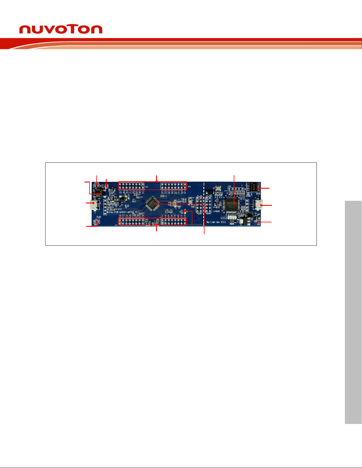
VDD (JP1)
Reset Button
(SW1)
I/O LED
Power LED
Target Chip
Virtual COM Port
Function Switch
(SW2)
ICE Controller
USB Connector
(J2)
ICE Controller
VCC : 3.3V or 5V
(JPR1)
Extended Connector (JP5, JP7)
GND (JP4)
Extended Connector (JP6, JP8)
USB Connector
(J3)
NuTiny-SDK-M4521 uses the M4521SE6AE as the target microcontroller. Figure 2-1 is NuTinySDK-M4521 for M4521 series, the left portion is called NuTiny-EVB-M4521 and the right portion is
Debug Adaptor called Nu-Link-Me.
NuTiny-EVB-M4521 is similar to other development boards. Users can use it to develop and verify
applications to emulate the real behavior. The on board chip covers M4521 series features. The
NuTiny-EVB-M4521 can be a real system controller to design users’ target systems.
Nu-Link-Me is a Debug Adaptor. The Nu-Link-Me Debug Adaptor connects your PC's USB port to
your target system (via Serial Wired Debug Port) and allows you to program and debug
embedded programs on the target hardware. The Nu-Link-Me V3.0 also supports VCOM function,
which gives users more flexibility when debug. To use Nu-Link-Me Debug adaptor with IAR or
Keil, please refer to “Nuvoton NuMicro
ICE driver user manual” in detail. These two documents will be stored in the local hard disk when
the user installs each driver. To use Nu-Link-Me 3.0 VCOM function, please refer to Chapter 5.
®
IAR ICE driver user manual “or Nuvoton NuMicro® Keil
M4521
Figure 2-1 NuTiny-SDK-M4521 (PCB Board)
Nov 28, 2018 Page 5 of 30 Rev 1.00
Page 6
NUTINY-SDK-M4521 USER MANUAL
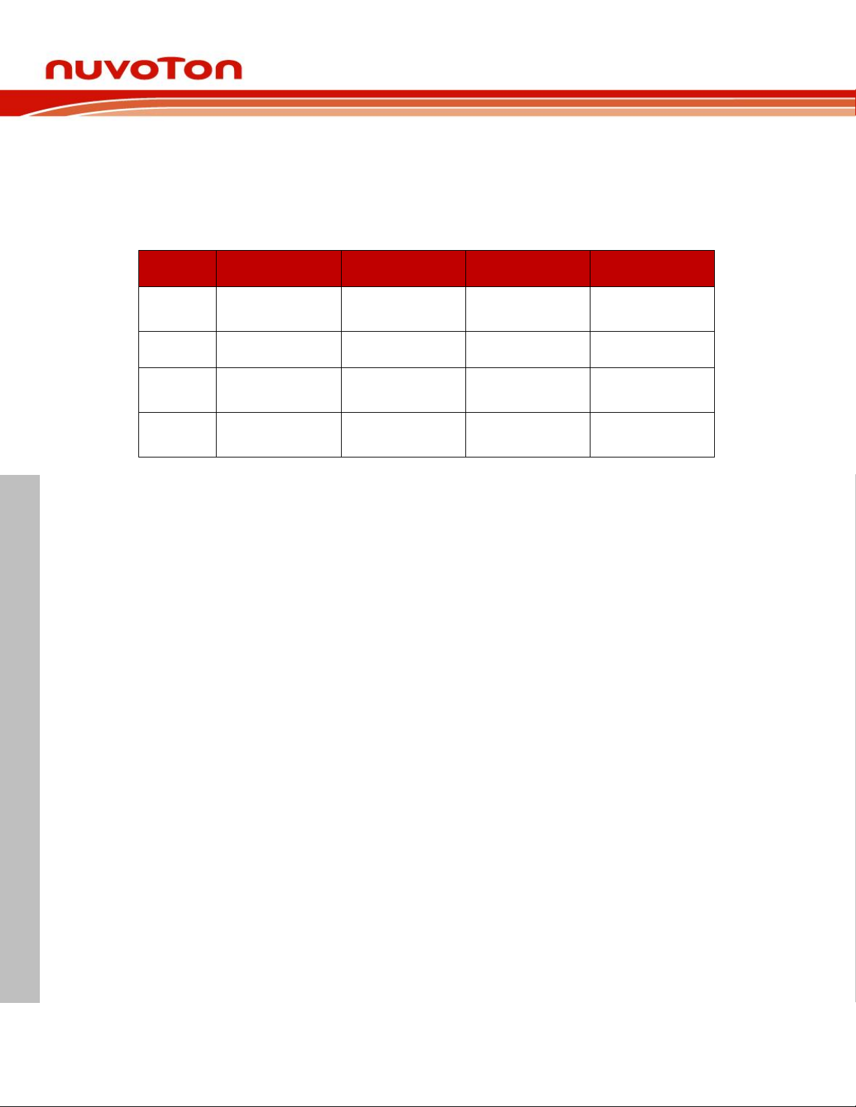
NuTiny -SDK-M4521 Jumper Description 2.1
Model
JPR1
JP1 VDD
J2 ICE USB Port
MCU Voltage
Model 1
Select 3.3V
(Default)
DC 3.3V Output
Connect to PC
DC 3.3V
Model 2
Select 5.0V
DC 5.0V Output
Connect to PC
DC 5.0V
Model 3
Select 3.3V or 5.0V
DC 2.5V ~ 5.0V
Input
Connect to PC
Voltage by JP1
Input
Model 4*
X
DC 2.5V ~ 5.0V
Input
X
Voltage by JP1
Input
2.1.1 Power Setting
JP1: VDD Voltage connecter in NuTiny-EVB-M4521
J2: USB port in Nu-Link-Me
JPR1: Select 5.0V or 3.3V for system power
X: Unused.
Note*: Need to separate NuTiny-EVB-M4521 and Nu-Link-Me.
M4521
2.1.2 Debug Connector
JP2: Connector in target board (NuTiny-EVB-M4521) for connecting with Nuvoton ICE
adaptor (Nu-Link-Me)
JP11: Connector in ICE adaptor (Nu-Link-Me) for connecting with a target board (NuTiny-
EVB-M4521)
2.1.3 USB Connector
J2: Micro USB Connector in Nu-Link-Me connected to a PC USB port
J3: Micro USB Connector in NuTiny-EVB-M4521 for application use
2.1.4 Extended Connector
JP5, JP6, JP7, and JP8: Show all chip pins in NuTiny-EVB-M4521
2.1.5 Reset Button
SW1: Reset button in NuTiny-EVB-M4521
2.1.6 Power Connector
JP1: VDD connector in NuTiny-EVB-M4521
JP4: GND connector in NuTiny-EVB-M4521
2.1.7 Virtual COM Port Function Switch
Nov 28, 2018 Page 6 of 30 Rev 1.00
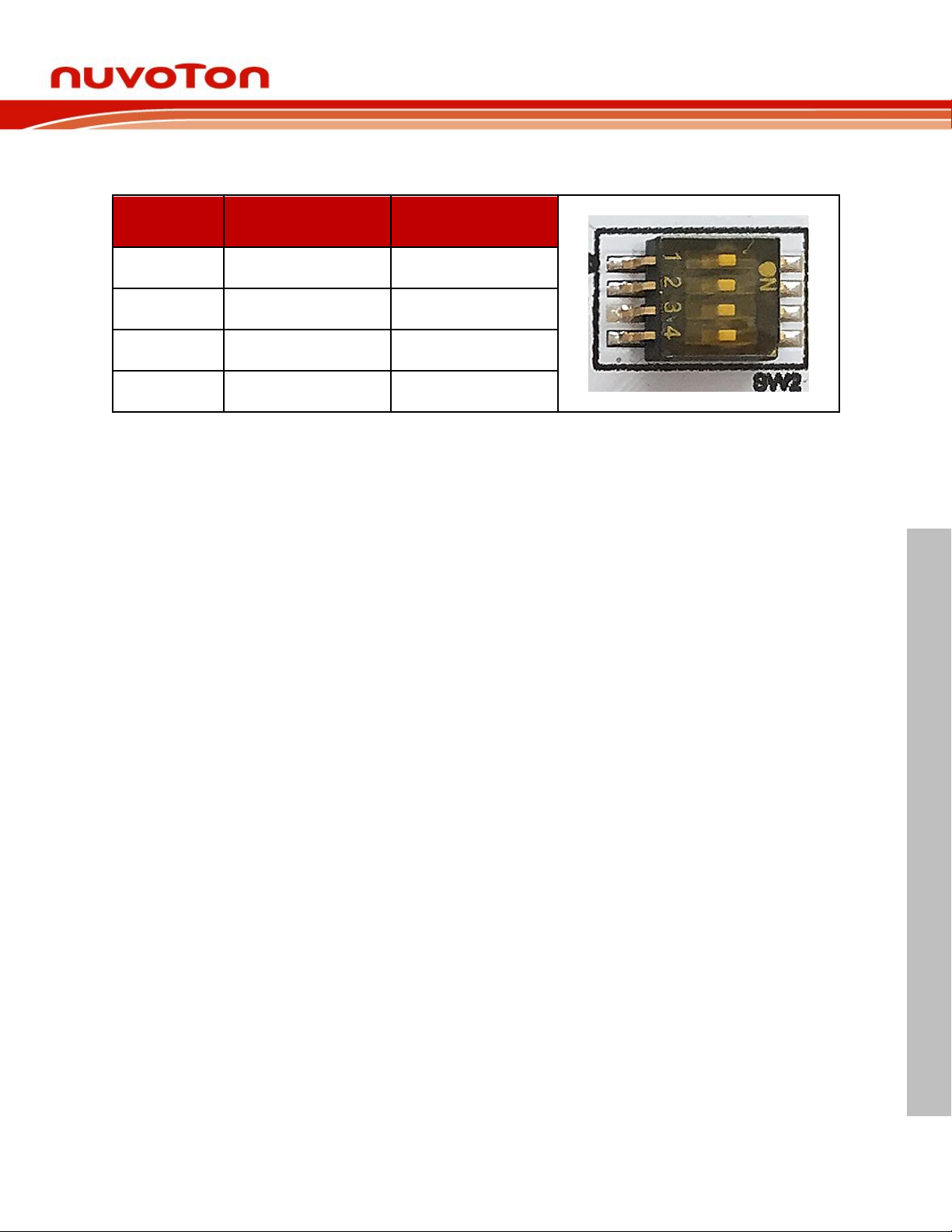
SW2: Switch SW2 on/off before power on to enable/disable VCOM function.
SW2 connects pin 6(PD.0/RXD) and pin 10(PD.1/TXD) in NuTiny-EVB-M4521 with pin
22(PB.1/TXD) and pin 21(PB.0/RXD) in Nuvoton ICE adaptor (Nu-Link-Me V3.0). SW2
Page 7
NUTINY-SDK-M4521 USER MANUAL
connects pin 30(VCOM) in Nuvoton ICE adaptor (Nu-Link-Me V3.0) to GND to enable VCOM
Switch Pin
Number
Disable VCOM Mode
Enable VCOM Mode
1
Off
On 2 Off
On 3 Off
On
4 X X
function.
X: Unused.
M4521
Nov 28, 2018 Page 7 of 30 Rev 1.00
Page 8
NUTINY-SDK-M4521 USER MANUAL
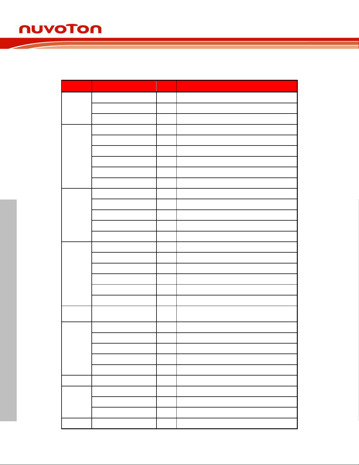
Pin Assignment for Extended Connector 2.2
Pin No.
Pin Name
Type
Description
1
PB.15
I/O
General purpose digital I/O pin.
EADC_CH12
A
EADC analog input channel 12.
EBI_nCS1
O
EBI chip select 1 enable output pin.
2
PB.5
I/O
General purpose digital I/O pin.
EADC_CH13
A
EADC analog input channel 13.
SPI0_MOSI0
I/O
SPI0 1st MOSI (Master Out, Slave In) pin.
SPI1_MOSI
I/O
SPI1 MOSI (Master Out, Slave In) pin.
EBI_AD6
I/O
EBI address/data bus bit 6.
UART2_RXD
I/O
Data receiver input pin for UART2.
3
PB.6
I/O
General purpose digital I/O pin.
EADC_CH14
A
EADC analog input channel 14.
SPI0_MISO0
I/O
SPI0 1st MISO (Master In, Slave Out) pin.
SPI1_MISO
I/O
SPI1 MISO (Master In, Slave Out) pin.
EBI_AD5
I/O
EBI address/data bus bit 5.
4
PB.7
I/O
General purpose digital I/O pin.
EADC_CH15
A
EADC analog input channel 15.
SPI0_CLK
I/O
SPI0 serial clock pin.
SPI1_CLK
I/O
SPI1 serial clock pin
EBI_AD4
I/O
EBI address/data bus bit 4.
STADC
I/O
ADC external trigger input.
5
nRESET
I
External reset input: active LOW, with an internal pull-up.
Set this pin low reset to initial state.
6
PD.0
I/O
General purpose digital I/O pin.
EADC_CH6
A
EADC analog input channel 6.
UART0_RXD
I
Data receiver input pin for UART0.
INT3 I External interrupt3 input pin.
T3
I/O
Timer3 event counter input / toggle output.
7
AVSS P Ground pin for analog circuit.
8
PD.8
I/O
General purpose digital I/O pin.
EADC_CH7
A
EADC analog input channel 7.
EBI_nCS0
O
EBI chip select 0 enable output pin.
9
PD.9
I/O
General purpose digital I/O pin.
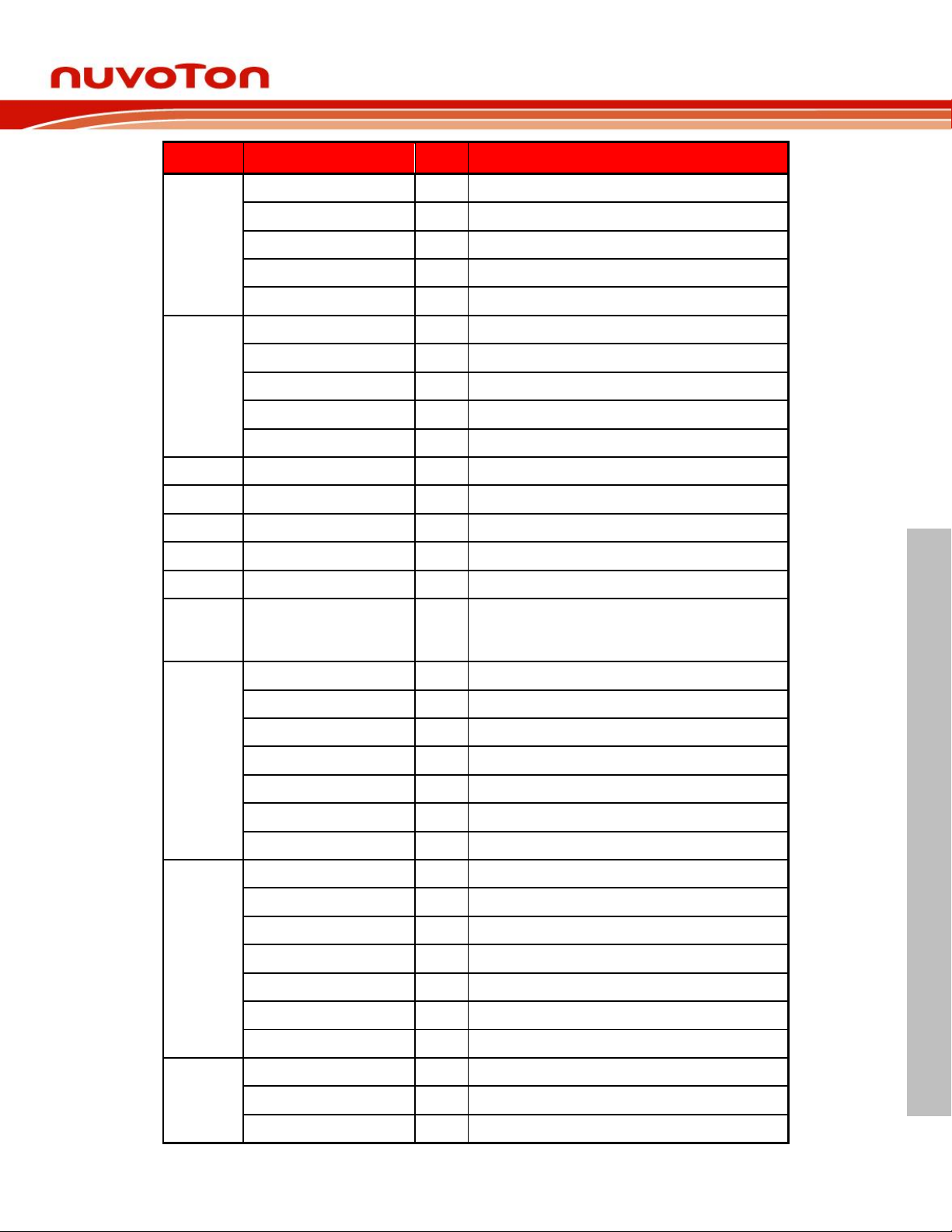
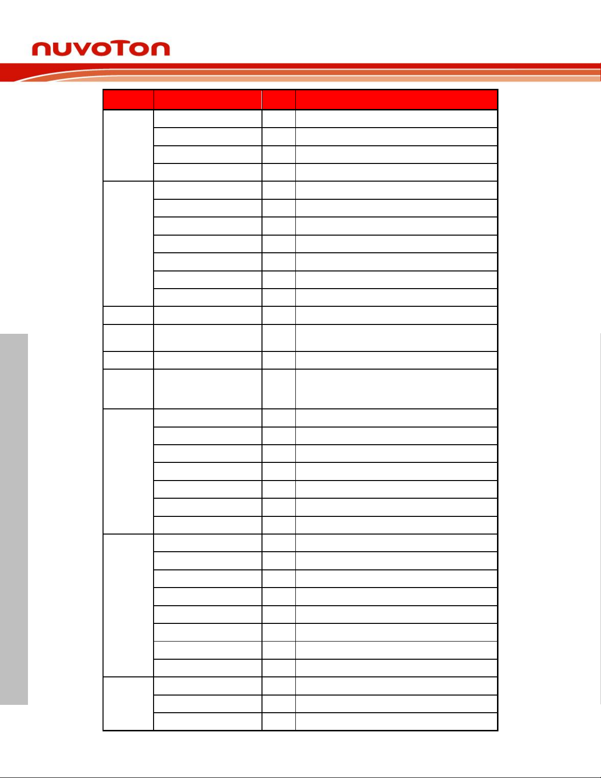
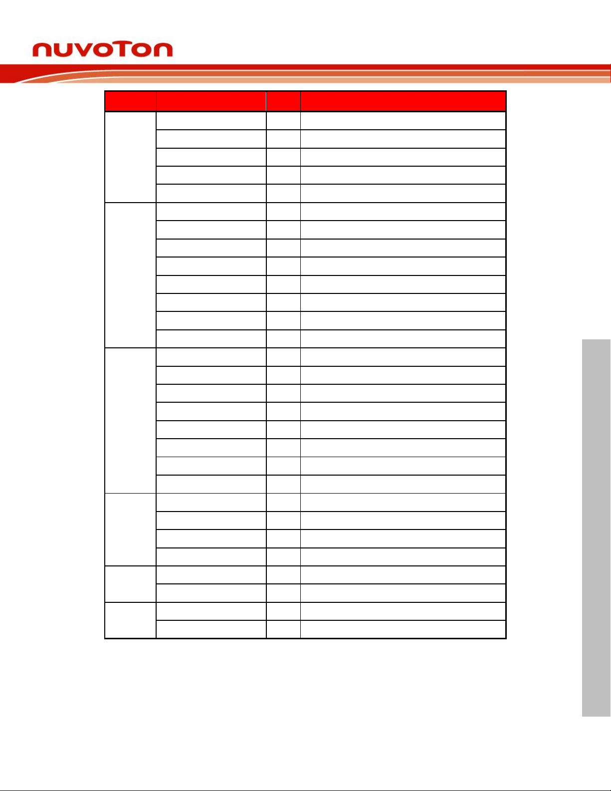
NuTiny-EVB-M4521 provides M4521SE6AE on board and the extended connector for LQFP64pin. Table 2-1 is the pin assignment for M4521SE6AE.
M4521
Nov 28, 2018 Page 8 of 30 Rev 1.00
Page 9
M4521
NUTINY-SDK-M4521 USER MANUAL
Pin No.
Pin Name
Type
Description
EADC_CH10
A
EADC analog input channel 10.
EBI_ALE
O
EBI address latch enable output pin.
10
PD.1
I/O
General purpose digital I/O pin.
EADC_CH11
A
EADC analog input channel 11.
PWM0_SYNC_IN
I
PWM0 counter synchronous trigger input pin.
UART0_TXD
O
Data transmitter output pin for UART0.
T0
I/O
Timer0event counter input / toggle output
EBI_nRD
O
EBI read enable output pin.
11
PD.2
I/O
General purpose digital I/O pin.
STADC
I
ADC external trigger input.
T0_EXT
I
Timer0 external capture input.
PWM0_BRAKE0
I
PWM0 break input 0
EBI_nWR
O
EBI write enable output pin.
INT0 I External interrupt0 input pin.
12
PD.3
I/O
General purpose digital I/O pin.
T2
I/O
Timer2 event counter input / toggle output
T1_EXT
I
Timer1 external capture input
PWM0_BRAKE1
I
PWM0 break input 1
EBI_MCLK
O
EBI external clock output pin
INT1 I External interrupt1 input pin.
13
V
BAT
Power supply by batteries for RTC and PF.0~PF.2.
14
PF.0
I/O
General purpose digital I/O pin.
X32_OUT
O
External 32.768 kHZ (low speed) crystal output pin.
INT5 I External interrupt5 input pin.
15
PF.1
I/O
General purpose digital I/O pin.
X32_IN
I
External 32.768 kHZ (low speed) crystal input pin.
16
PF.2
I/O
General purpose digital I/O pin.
TAMPER
I/O
TAMPER detector loop pin
17
PD.12
I/O
General purpose digital I/O pin.
UART3_TXD
O
Data transmitter output pin for UART3.
PWM1_CH0
I/O
PWM1 output/capture input.
EBI_ADR16
O
EBI address bus bit 16.
18
PD.13
I/O
General purpose digital I/O pin.
UART3_RXD
I
Data receiver input pin for UART3.
Nov 28, 2018 Page 9 of 30 Rev 1.00
Page 10
M4521
NUTINY-SDK-M4521 USER MANUAL
Pin No.
Pin Name
Type
Description
PWM1_CH1
I/O
PWM1 output/capture input.
EBI_ADR17
O
EBI address bus bit 17.
19
PD.14
I/O
General purpose digital I/O pin.
UART3_nCTS
I
Clear to Send input pin for UART3.
PWM1_CH2
I/O
PWM1 output/capture input.
EBI_ADR18
O
EBI address bus bit 18.
20
PD.15
I/O
General purpose digital I/O pin.
UART3_nRTS
O
Request to Send output pin for UART3.
PWM1_CH3
I/O
PWM1 output/capture input.
EBI_ADR19
O
EBI address bus bit 19.
21
PD.7
I/O
General purpose digital I/O pin.
PWM0_SYNC_IN
I
PWM0 counter synchronous trigger input pin.
T1
I/O
Timer1 event counter input / toggle output
PWM0_CH5
I/O
PWM0 output/capture input.
EBI_nRD
O
EBI read enable output pin.
22
PF.3
I/O
General purpose digital I/O pin.
XT1_OUT
O
External 4~20 MHz (high speed) crystal output pin.
I2C1_SCL
I/O
I2C1 clock pin.
23
PF.4
I/O
General purpose digital I/O pin.
XT1_IN
I
External 4~20 MHz (high speed) crystal input pin.
I2C1_SDA
I/O
I2C1 data input/output pin.
24
VSS A Ground pin for digital circuit.
25
VDD
A
Power supply for I/O ports and LDO source for internal
PLL and digital function.
26
LDO_CAP
A
LDO output pin.
Note: This pin needs to be connected with a 1uF
capacitor.
27
PC.0
I/O
General purpose digital I/O pin.
SPI1_CLK
I/O
SPI1 serial clock pin.
UART2_nCTS
I
Clear to Send input pin for UART2.
PWM0_CH0
I/O
PWM0 output/capture input.
EBI_AD8
I/O
EBI address/data bus bit 8.
INT2 I External interrupt2 input pin.
UART3_TXD
O
Data transmitter output pin for UART3.
T3_EXT
I
Timer3 external capture input.
28
PC.1
I/O
General purpose digital I/O pin.
Nov 28, 2018 Page 10 of 30 Rev 1.00
Page 11
M4521
NUTINY-SDK-M4521 USER MANUAL
Pin No.
Pin Name
Type
Description
CLKO
O
Clock Out
UART2_nRTS
O
Request to Send output pin for UART2.
PWM0_CH1
I/O
PWM0 output/capture input.
EBI_AD9
I/O
EBI address/data bus bit 9.
UART3_RXD
I/O
Data receiver input pin for UART3.
29
PC.2
I/O
General purpose digital I/O pin.
SPI1_SS
I
SPI1 slave select pin.
UART2_TXD
O
Data transmitter output pin for UART2.
PWM0_CH2
I/O
PWM0 output/capture input.
EBI_AD10
I/O
EBI address/data bus bit 10.
30
PC.3
I/O
General purpose digital I/O pin.
SPI1_MOSI
I/O
SPI1 MOSI (Master Out, Slave In) pin.
UART2_RXD
I
Data receiver input pin for UART2.
PWM0_CH3
I/O
PWM0 output/capture input.
EBI_AD11
I/O
EBI address/data bus bit 11.
31
PC.4
I/O
General purpose digital I/O pin.
SPI1_MISO
I/O
SPI1 MISO (Master In, Slave Out) pin.
I2C1_SCL
I/O
I2C1 clock pin.
PWM0_CH4
I/O
PWM0 output/capture input.
EBI_AD12
I/O
EBI address/data bus bit 12.
32
PC.5
I/O
General purpose digital I/O pin.
PWM0_CH5
I/O
PWM0 output/capture input.
EBI_AD13
I/O
EBI address/data bus bit 13.
33
PC.6
I/O
General purpose digital I/O pin.
I2C1_SMBAL
O
I2C1 SMBus SMBALTER# pin
PWM1_CH0
I/O
PWM1 output/capture input.
EBI_AD14
I/O
EBI address/data bus bit 14.
UART0_TXD
O
Data transmitter output pin for UART0.
34
PC.7
I/O
General purpose digital I/O pin.
I2C1_SMBSUS
O
I2C1 SMBus SMBSUS# pin (PMBus CONTROL pin)
PWM1_CH1
I/O
PWM1 output/capture input.
EBI_AD15
I/O
EBI address/data bus bit 15.
UART0_RXD
I
Data receiver input pin for UART0.
35
PF.5
I/O
General purpose digital I/O pin.
Nov 28, 2018 Page 11 of 30 Rev 1.00
Page 12
M4521
NUTINY-SDK-M4521 USER MANUAL
Pin No.
Pin Name
Type
Description
ICE_CLK
I
Serial wired debugger clock pin
36
PF.6
I/O
General purpose digital I/O pin.
ICE_DAT
I/O
Serial wired debugger data pin
37
PE.8
I/O
General purpose digital I/O pin.
UART1_TXD
O
Data transmitter output pin for UART1.
SPI0_MISO1
I/O
SPI0 2nd MISO (Master In, Slave Out) pin.
I2C1_SCL
I/O
I2C1 clock pin.
SC0_PWR
O
SmartCard power pin.
CLKO
O
Clock Out
PWM0_BRAKE0
I
PWM0 break input 0
T1
I/O
Timer1 event counter input / toggle output
38
PE.9
I/O
General purpose digital I/O pin.
UART1_RXD
I
Data receiver input pin for UART1.
SPI0_MOSI1
I/O
SPI0 2nd MOSI (Master Out, Slave In) pin.
I2C1_SDA
I/O
I2C1 data input/output pin.
SC0_RST
O
SmartCard reset pin.
PWM1_BRAKE1
I
PWM1 break input 1
T2
I/O
Timer2 event counter input / toggle output
39
PE.10
I/O
General purpose digital I/O pin.
SPI1_MISO
I/O
SPI1 MISO (Master In, Slave Out) pin.
SPI0_MISO0
I/O
SPI0 1st MISO (Master In, Slave Out) pin.
UART1_nCTS
I
Clear to Send input pin for UART1.
I2C0_SMBAL
O
I2C0 SMBus SMBALTER# pin
SC0_DAT
I/O
SmartCard data pin.
UART3_TXD
O
Data transmitter output pin for UART3.
I2C1_SCL
I/O
I2C1 clock pin.
40
PE.11
I/O
General purpose digital I/O pin.
SPI1_MOSI
I/O
SPI1 MOSI (Master Out, Slave In) pin.
SPI0_MOSI0
I/O
SPI0 1st MOSI (Master Out, Slave In) pin.
UART1_nRTS
O
Request to Send output pin for UART1.
I2C0_SMBSUS
O
I2C0 SMBus SMBSUS# pin (PMBus CONTROL pin)
SC0_CLK
O
SmartCard clock pin.
UART3_RXD
I
Data receiver input pin for UART3.
I2C1_SDA
I/O
I2C1 data input/output pin.
Nov 28, 2018 Page 12 of 30 Rev 1.00
Page 13
M4521
NUTINY-SDK-M4521 USER MANUAL
Pin No.
Pin Name
Type
Description
41
PE.12
I/O
General purpose digital I/O pin.
SPI1_SS
I/O
SPI1 slave select pin
SPI0_SS
I/O
SPI0 slave select pin.
UART1_TXD
O
Data transmitter output pin for UART1.
I2C0_SCL
I/O
I2C0 clock pin.
42
PE.13
I/O
General purpose digital I/O pin.
SPI1_CLK
I/O
SPI1 serial clock pin
SPI0_CLK
I/O
SPI0 serial clock pin.
UART1_RXD
I
Data receiver input pin for UART1.
I2C0_SDA
I/O
I2C0 data input/output pin.
43
V
DDIO
A Power supply for PE.8~PE.13.
44
USB_VBUS
A
Power supply from USB* host or HUB.
45
USB_D-
I
USB differential signal D-.
46
USB_D+
I
USB differential signal D+.
47
PF.7
I/O
General purpose digital I/O pin.
48
USB_VDD33_CAP
A
Internal power regulator output 3.3V decoupling pin.
Note: This pin needs to be connected with a 1uF
capacitor.
49
PA.3
I/O
General purpose digital I/O pin.
UART0_RXD
I
Data receiver input pin for UART0.
UART0_nRTS
O
Request to Send output pin for UART0.
I2C0_SCL
I/O
I2C0 clock pin.
SC0_PWR
O
SmartCard power pin.
PWM1_CH2
I/O
PWM1 output/capture input.
EBI_AD3
I/O
EBI address/data bus bit 3.
50
PA.2
I/O
General purpose digital I/O pin.
UART0_TXD
O
Data transmitter output pin for UART0.
UART0_nCTS
I
Clear to Send input pin for UART0.
I2C0_SDA
I/O
I2C0 data input/output pin.
SC0_RST
O
SmartCard reset pin.
PWM1_CH3
I/O
PWM1 output/capture input.
EBI_AD2
I/O
EBI address/data bus bit 2.
51
PA.1
I/O
General purpose digital I/O pin.
UART1_nRTS
O
Request to Send output pin for UART1.
UART1_RXD
I
Data receiver input pin for UART1.
Nov 28, 2018 Page 13 of 30 Rev 1.00
Page 14
M4521
NUTINY-SDK-M4521 USER MANUAL
Pin No.
Pin Name
Type
Description
SC0_DAT
I/O
SmartCard data pin.
PWM1_CH4
I/O
PWM1 output/capture input.
EBI_AD1
I/O
EBI address/data bus bit 1.
STADC
I/O
ADC external trigger input.
52
PA.0
I/O
General purpose digital I/O pin.
UART1_nCTS
I
Clear to Send input pin for UART1.
UART1_TXD
O
Data transmitter output pin for UART1.
SC0_CLK
O
SmartCard clock pin.
PWM1_CH5
I/O
PWM1 output/capture input.
EBI_AD0
I/O
EBI address/data bus bit 0.
INT0 I External interrupt0 input pin.
53
VSS A Ground pin for digital circuit.
54
VDD
A
Power supply for I/O ports and LDO source for internal
PLL and digital function.
55
AVDD A Power supply for internal analog circuit.
56
V
REF
I Voltage reference input for ADC.
Note: This pin needs to be connected with a 1uF
capacitor.
57
PB.0
I/O
General purpose digital I/O pin.
EADC_CH0
A
EADC analog input.
SPI0_MOSI1
I/O
SPI0 2nd MOSI (Master Out, Slave In) pin.
UART2_RXD
I
Data receiver input pin for UART2.
T2
I/O
Timer2 event counter input / toggle output
EBI_nWRL
O
EBI low byte write enable output pin.
INT1 I External interrupt1 input pin.
58
PB.1
I/O
General purpose digital I/O pin.
EADC_CH1
A
EADC analog input channel 1.
SPI0_MISO1
I/O
SPI0 2nd MISO (Master In, Slave Out) pin.
UART2_TXD
O
Data transmitter output pin for UART2.
T3
I/O
Timer3 event counter input / toggle output
SC0_RST
O
SmartCard reset pin.
PWM0_SYNC_OUT
O
PWM0 counter synchronous trigger output pin.
EBI_nWRH
O
EBI high byte write enable output pin
59
PB.2
I/O
General purpose digital I/O pin.
EADC_CH2
A
EADC analog input channel 2.
SPI0_CLK
I/O
SPI0 serial clock pin.
Nov 28, 2018 Page 14 of 30 Rev 1.00
Page 15
M4521
NUTINY-SDK-M4521 USER MANUAL
Pin No.
Pin Name
Type
Description
SPI1_CLK
I/O
SPI1 serial clock pin
UART1_RXD
I
Data receiver input pin for UART1.
SC0_CD
I
SmartCard card detect pin.
UART3_RXD
I
Data receiver input pin for UART3.
T2_EXT
I
Timer2 external capture input.
60
PB.3
I/O
General purpose digital I/O pin.
EADC_CH3
A
EADC analog input channel 3.
SPI0_MISO0
I/O
SPI0 1st MISO (Master In, Slave Out) pin.
SPI1_MISO
I/O
SPI1 MISO (Master In, Slave Out) pin.
UART1_TXD
O
Data transmitter output pin for UART1.
EBI_ALE
O
EBI address latch enable output pin.
UART3_TXD
O
Data transmitter output pin for UART3.
T0_EXT
I
Timer0 external capture input.
61
PB.4
I/O
General purpose digital I/O pin.
EADC_CH4
A
EADC analog input channel 4.
SPI0_SS
I/O
SPI0 slave select pin.
SPI1_SS
I/O
SPI1 slave select pin
UART1_nCTS
I
Clear to Send input pin for UART1.
EBI_AD7
I/O
EBI address/data bus bit 7.
UART2_TXD
O
Data transmitter output pin for UART2.
T1_EXT
I
Timer1 external capture input.
62
PB.8
I/O
General purpose digital I/O pin.
EADC_CH5
A
EADC analog input channel 5.
UART1_nRTS
O
Request to Send output pin for UART1.
PWM0_CH2
I/O
PWM0 output/capture input.
63
PB.11
I/O
General purpose digital I/O pin.
EADC_CH8
A
EADC analog input channel 8.
64
PB.12
I/O
General purpose digital I/O pin.
EADC_CH9
A
EADC analog input channel 9.
Nov 28, 2018 Page 15 of 30 Rev 1.00
Table 2-1 Pin Assignment for M4521
Page 16
NUTINY-SDK-M4521 USER MANUAL
NuTiny-SDK-M4521 PCB Placement 2.3
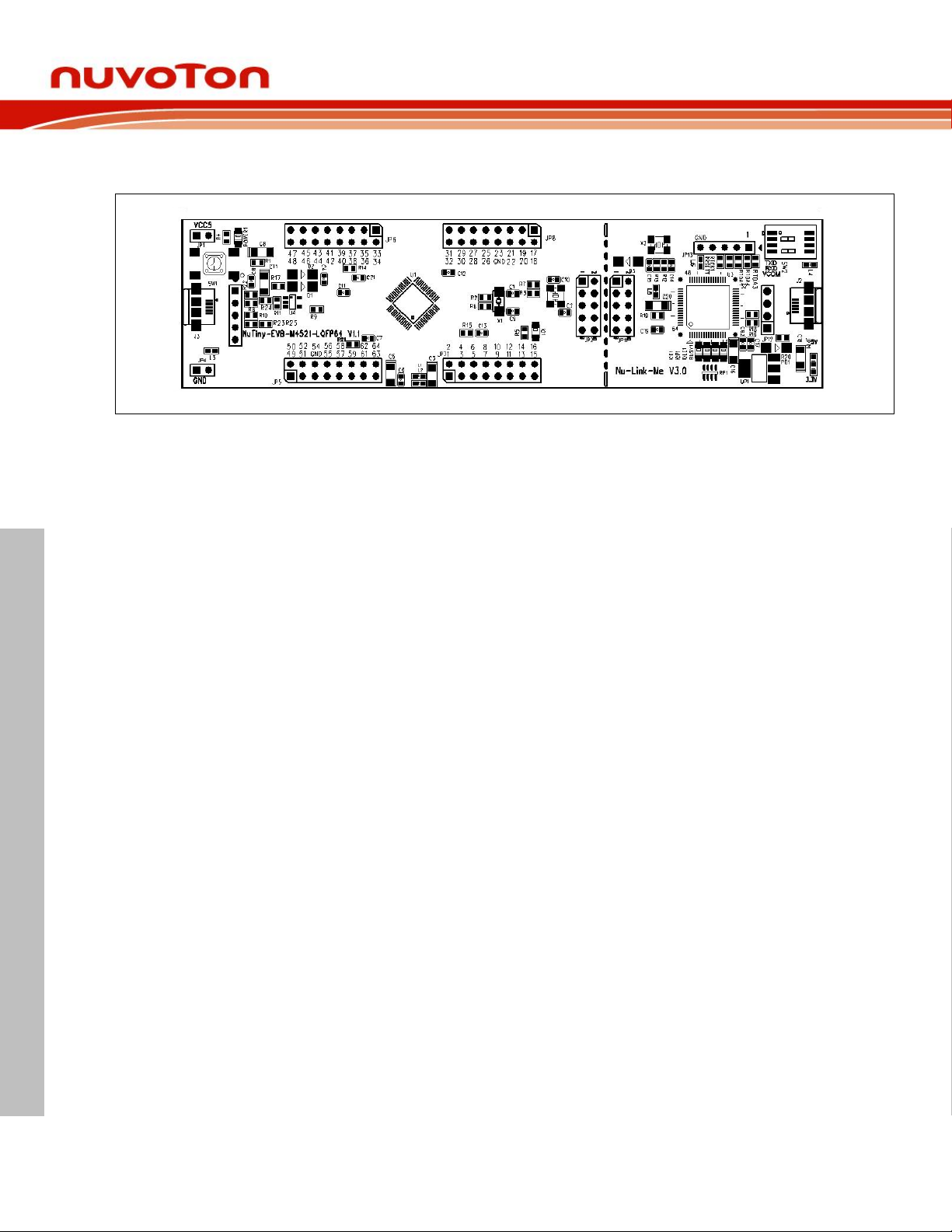
Users can refer to Figure 2-2 for the NuTiny-SDK-M4521 PCB placement.
Figure 2-2 NuTiny-SDK-M4521 PCB Placement
M4521
Nov 28, 2018 Page 16 of 30 Rev 1.00
Page 17
NUTINY-SDK-M4521 USER MANUAL
3 HOW TO START NUTINY-SDK-M4521 ON THE KEIL ΜVISION® IDE
Keil uVision® IDE Software Download and Install 3.1
Please visit the Keil company website (http://www.keil.com) to download the Keil μVision® IDE
and install the RVMDK.
Nuvoton Nu-Link Driver Download and Install 3.2
Please visit the Nuvoton company NuMicro® website (http://www.nuvoton.com/NuMicro) to
download “NuMicro
downloaded, please unzip the file and execute the “Nu-Link_Keil_Driver.exe” to install the driver.
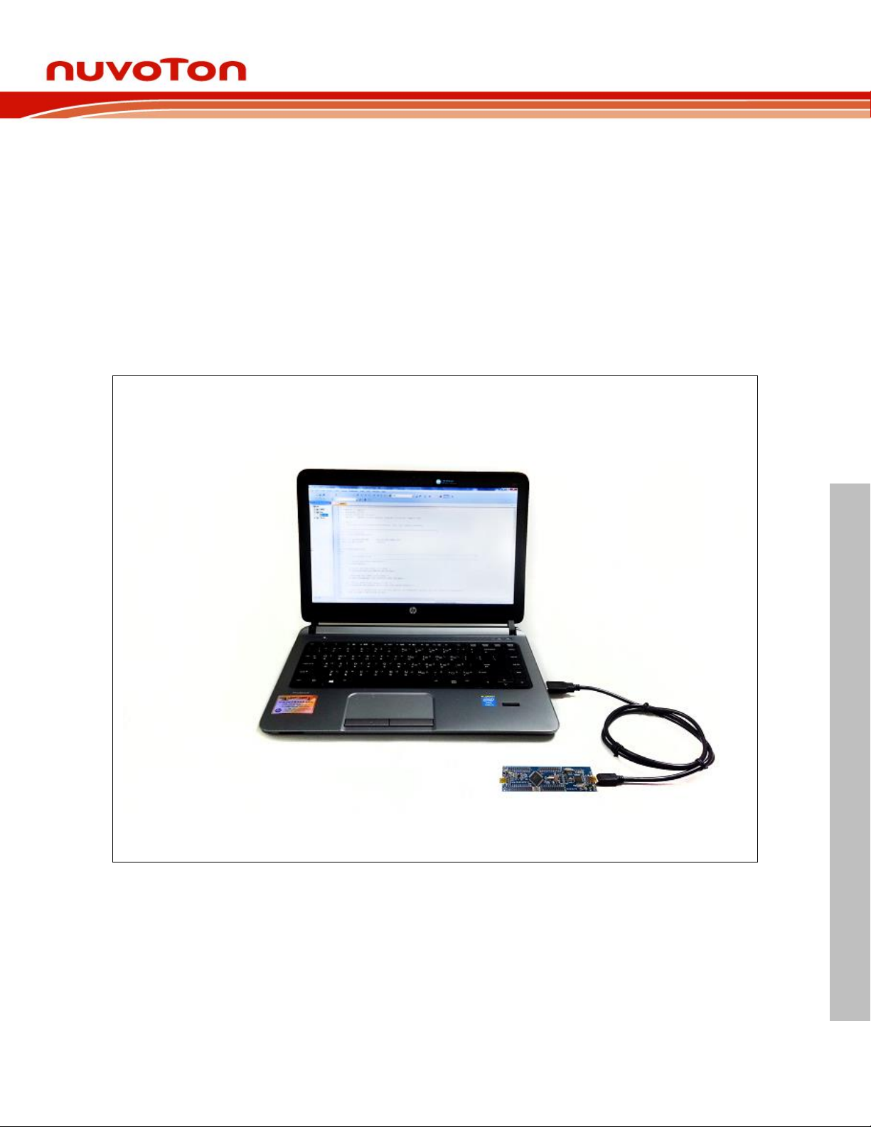
Hardware Setup
3.3
The hardware setup is shown as Figure 3-1.
®
Keil μVision® IDE driver” file. When the Nu-Link driver has been well
M4521
Figure 3-1 NuTiny-SDK-M4521 Hardware Setup
Nov 28, 2018 Page 17 of 30 Rev 1.00
Page 18
NUTINY-SDK-M4521 USER MANUAL
Example Program 3.4
Directory
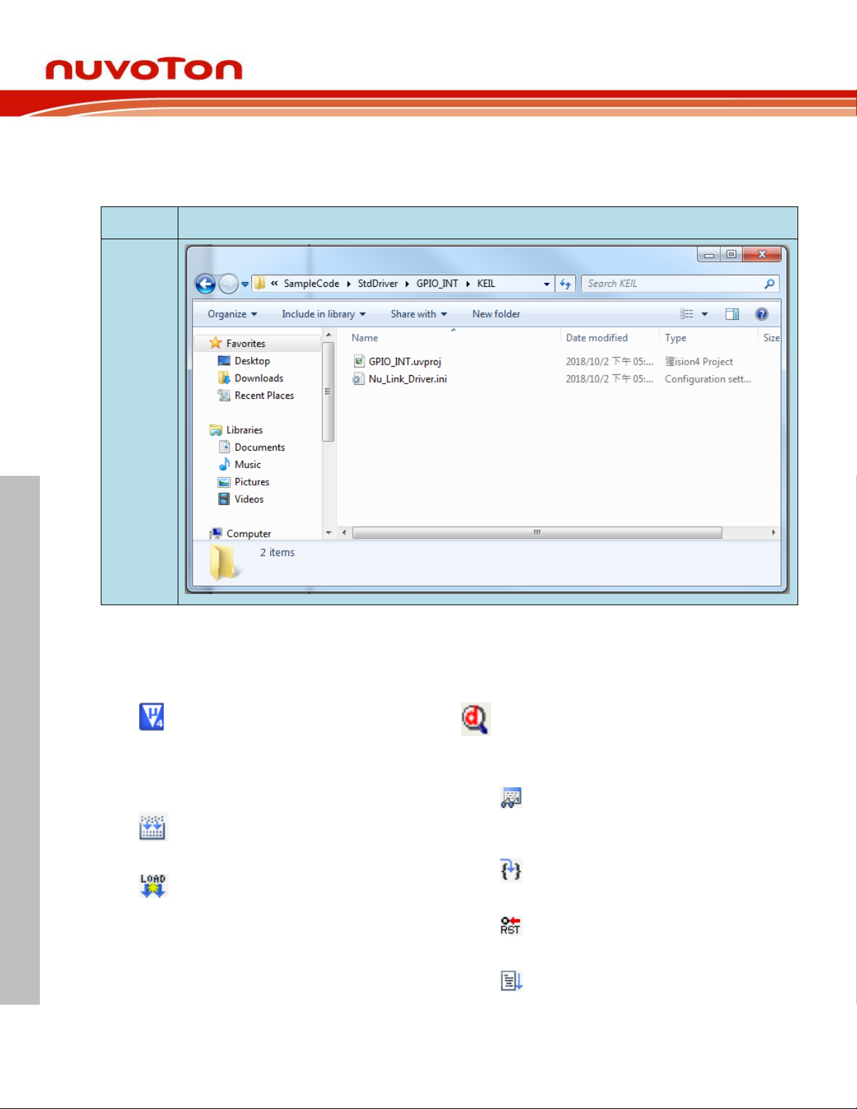
\\M4521_BSP_CMSIS_V3.00.000\SampleCode\StdDriver\GPIO_INT\KEIL
Project
File
Start μVision®
Project-Open
Open the SYS.uvproj project file
Project - Build
Compile and link the SYS application
Flash – Download
Program the application code into onchip Flash ROM
Start debug mode
Using the debugger commands, you
may:
Review variables in the watch
window
Single step through code
Reset the device
Run the application
This example demonstrates the ease of downloading and debugging an application on a NuTinySDK-M4521 board. It can be found on Figure 3-2 list directory and downloaded from Nuvoton
NuMicro® website.
M4521
To use this example:
This sample code runs some functions about system manager controller and clock controller, and
will show messages by Uart. Users can see the messages by following the steps of Chapter 5.
Nov 28, 2018 Page 18 of 30 Rev 1.00
Figure 3-2 Example Directory
Page 19
NUTINY-SDK-M4521 USER MANUAL
4 HOW TO START NUTINY-SDK-M4521 ON THE IAR EMBEDDED
WORKBENCH
IAR Embedded Workbench Software Download and Install 4.1
Please connect to IAR company website (http://www.iar.com) to download the IAR Embedded
Workbench and install the EWARM.
Nuvoton Nu-Link Driver Download and Install 4.2
Please visit the Nuvoton company NuMicro® website (http://www.nuvoton.com/NuMicro ) to
download the “NuMicro® IAR EWARM Driver” file. When the Nu-Link driver has been well
downloaded, please unzip the file and execute the “Nu-Link_Keil_Driver.exe” to install the
driver.
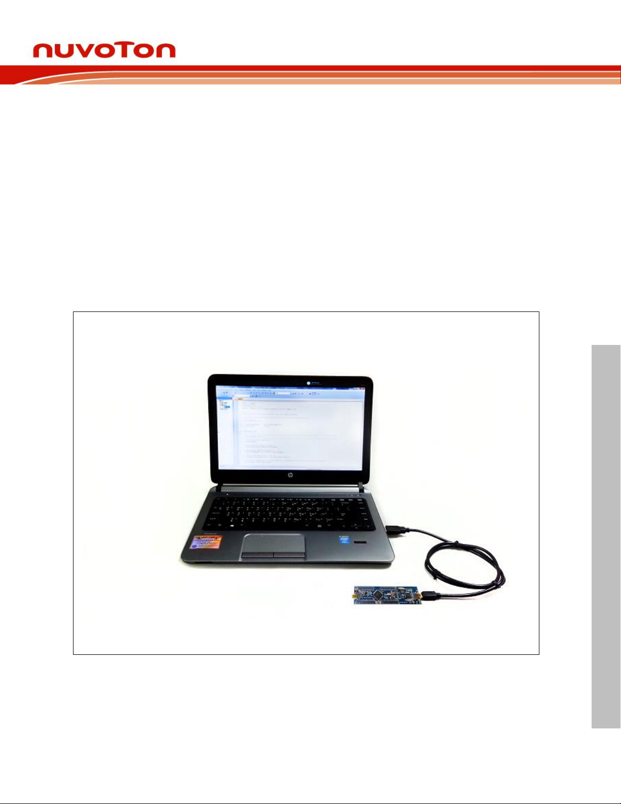
Hardware Setup 4.3
The hardware setup is shown as Figure 4-1.
M4521
Figure 4-1 NuTiny-SDK-M4521 Hardware Setup
Nov 28, 2018 Page 19 of 30 Rev 1.00
Page 20
NUTINY-SDK-M4521 USER MANUAL
Example Program 4.4
Directory
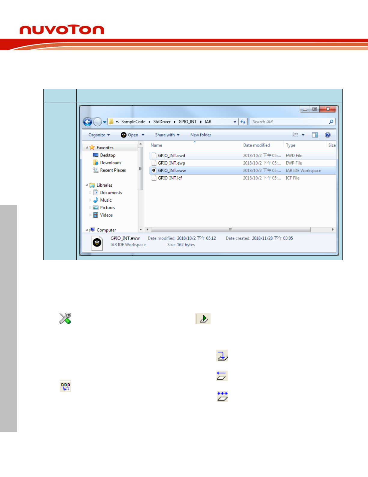
\\M4521_BSP_CMSIS_V3.00.000\SampleCode\StdDriver\GPIO_INT\IAR
Project
File
Start IAR Embedded Workbench
Project – Download and Debug
Program the application code into on-chip
Flash ROM
File-Open-Workspace
Open the SYS.eww workspace file
Single step through code
Project - Make
Compile and link the SYS application
Reset the device
Run the application
This example demonstrates the ease of downloading and debugging an application on a
NuTiny-SDK-M4521 board. It can be found on Figure 4-2 list directory and downloaded from
Nuvoton NuMicro® website.
M4521
Figure 4-2 Example Directory
To use this example:
This sample code runs some functions about system manager controller and clock controller, and
will show messages by Uart. Users can see the messages by following the steps of Chapter 5.
Nov 28, 2018 Page 20 of 30 Rev 1.00
Page 21
NUTINY-SDK-M4521 USER MANUAL
5 STARTING TO USE NU-LINK-ME 3.0 VCOM FUNCTION
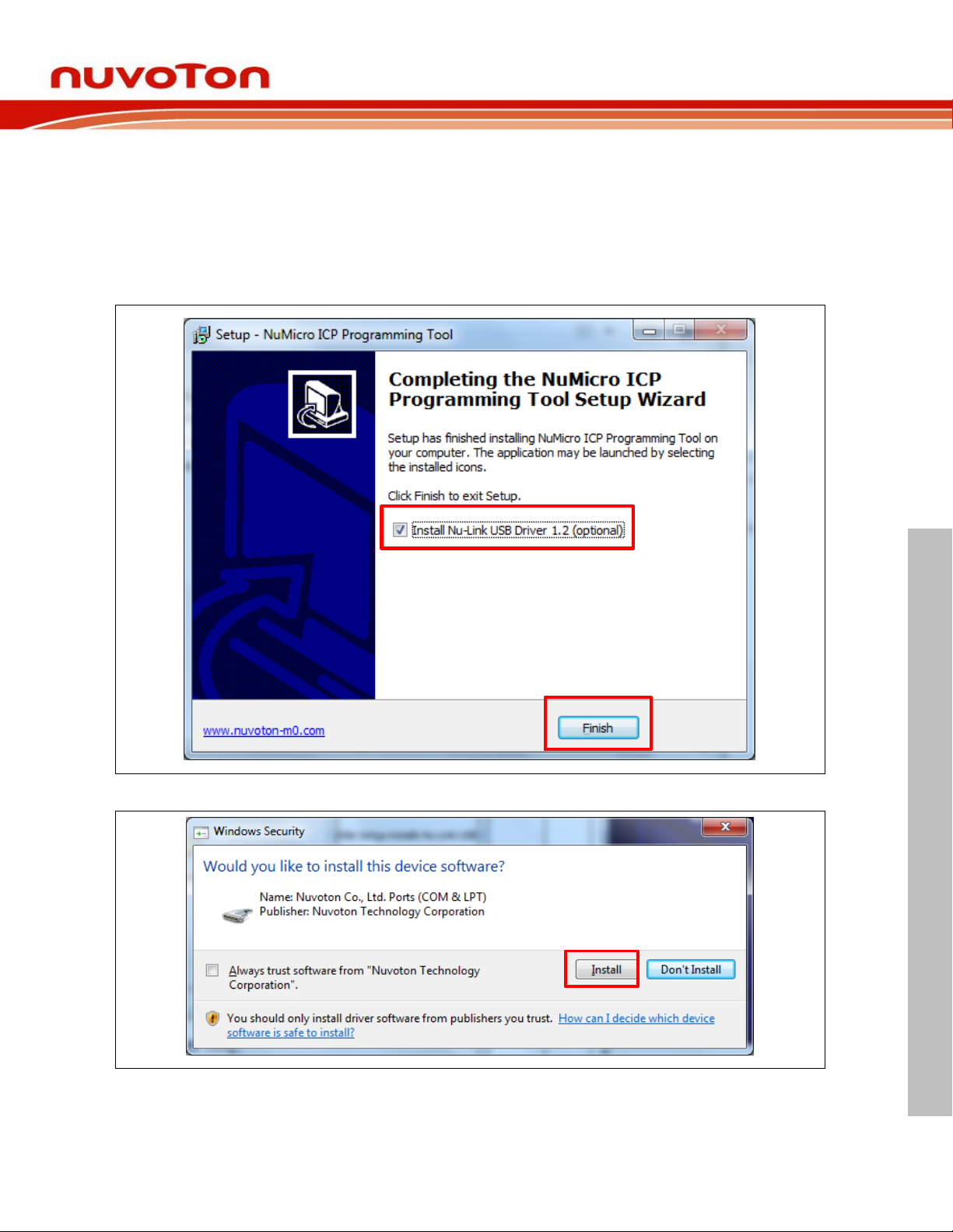
Downloading and Installing VCOM Driver 5.1
Please connect to Nuvoton NuMicro® website (http://www.nuvoton.com/NuMicro) to download
the “NuMicro
downloaded, please unzip the file and execute the “ICP Programming Tool.exe”. Simply follow
the installation and optional steps to install ICP Programming Tool and Nu-Link USB Driver,
which included VCOM driver.
®
ICP Programming Tool” file. After the ICP Programming Tool driver is
M4521
Nov 28, 2018 Page 21 of 30 Rev 1.00
Figure 5-1 Optional Step after ICP Programming Tool Installation
Figure 5-2 Install Nuvoton COM&LPT Driver
Page 22
NUTINY-SDK-M4521 USER MANUAL
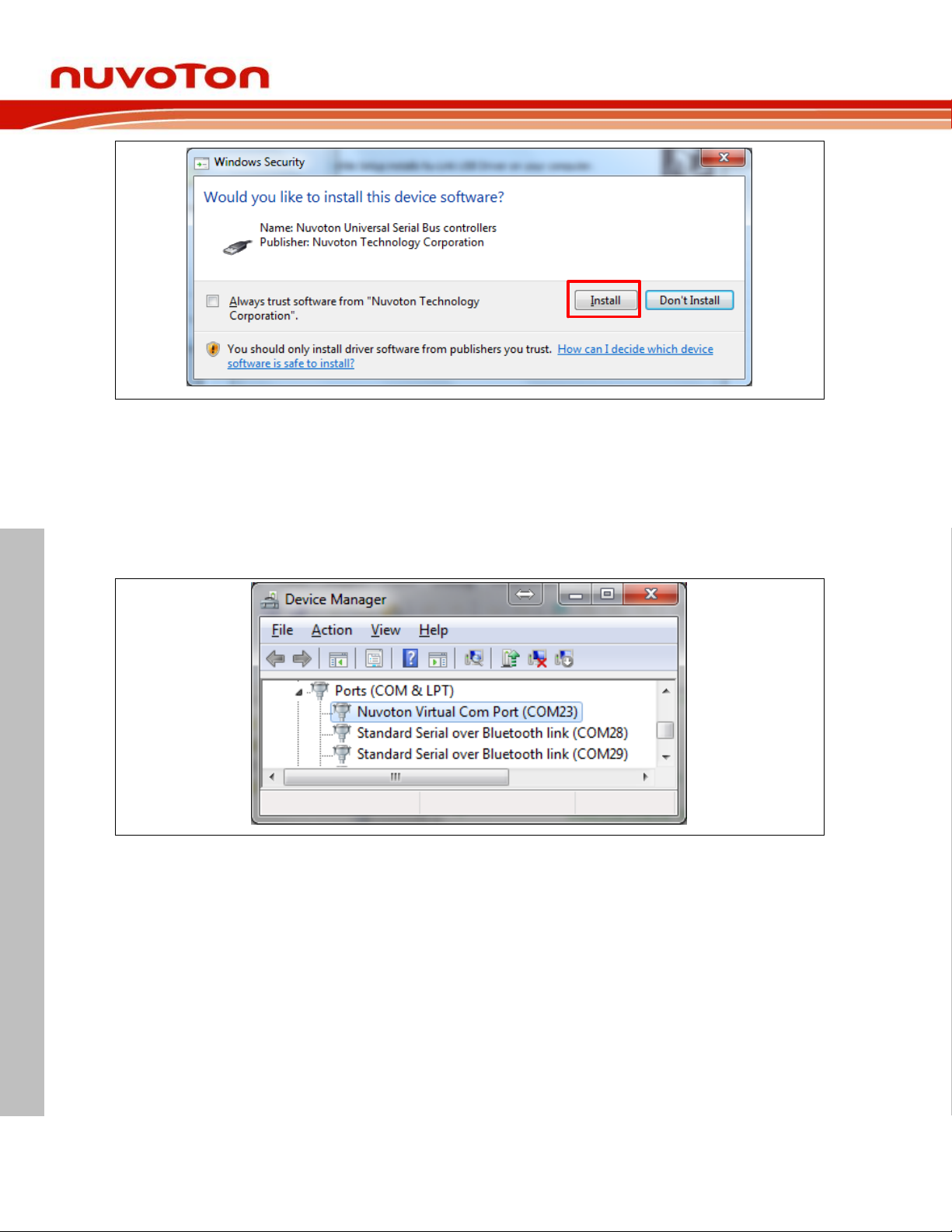
Figure 5-3 Install Nuvoton Universal Serial Bus Controllers
VCOM Mode Setting on NuTiny-SDK-M4521 5.2
Before the NuTiny-SDK-M4521 is connected to the PC, please enable SW2 VCOM function by
switching on SW2. The NuTiny-EVB-M4521 transmits through UART0 to VCOM to send out
data. Switch SW2 off when using UART0 function without VCOM function.
M4521
After connected USB port in Nu-Link-Me to the PC, user can find a “Nuvoton Virtual Com Port”
from Device Manager as Figure 5-4.
Figure 5-4 Nuvoton Virtual Com Port
Setup on the Development Tool 5.3
The example is demonstrated on the Keil μVision® IDE.
5.3.1 Check the Using UART on the Keil μVision® IDE
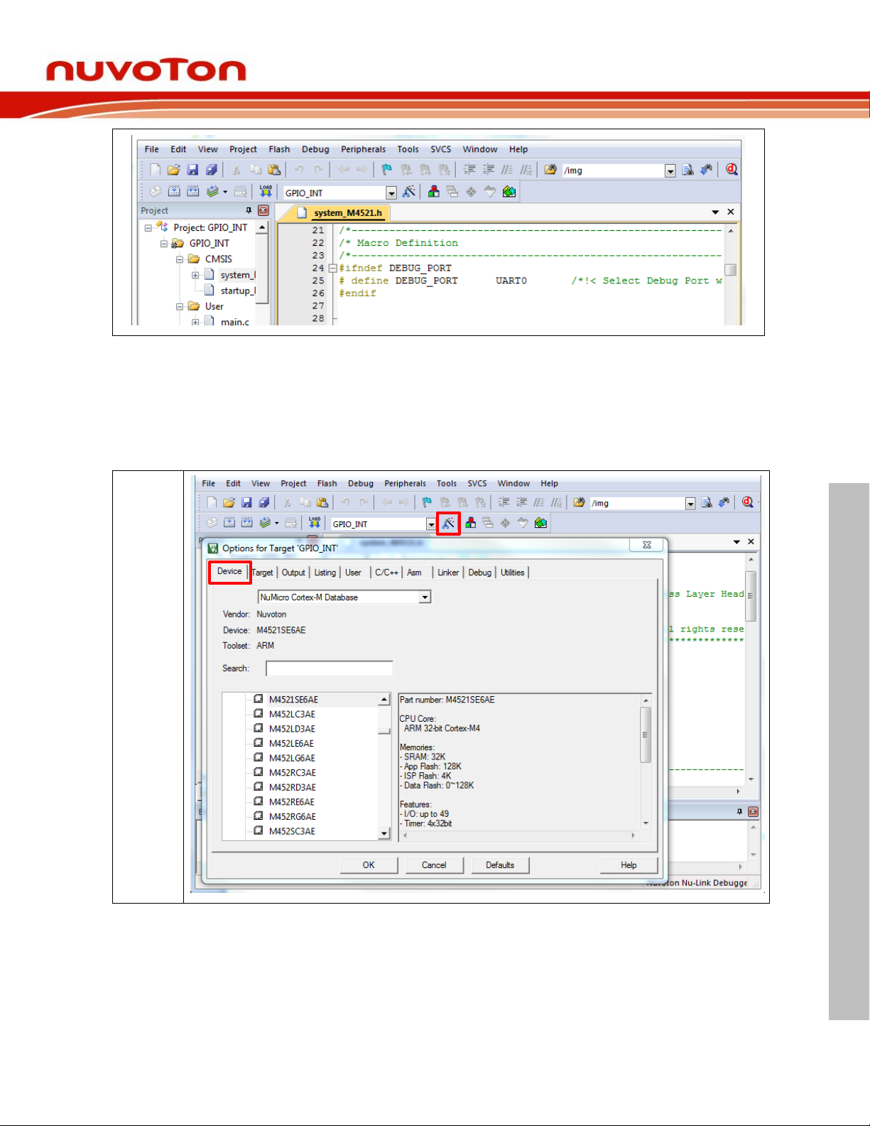
Please open the project and find system_M4521.h (which can be found in
\\M4521_BSP_CMSIS_V3.00.000\Library\Device\Nuvoton\M4521\Include) to check the using
UART in DEBUG_PORT. The setting has to be the same as the using UART in the NuTinyEVB-M4521.
Nov 28, 2018 Page 22 of 30 Rev 1.00
Page 23
NUTINY-SDK-M4521 USER MANUAL
Figure 5-5 The Using UART on Keil μVision® IDE
Step 1
5.3.2 Check the Target Device and Debug Setting
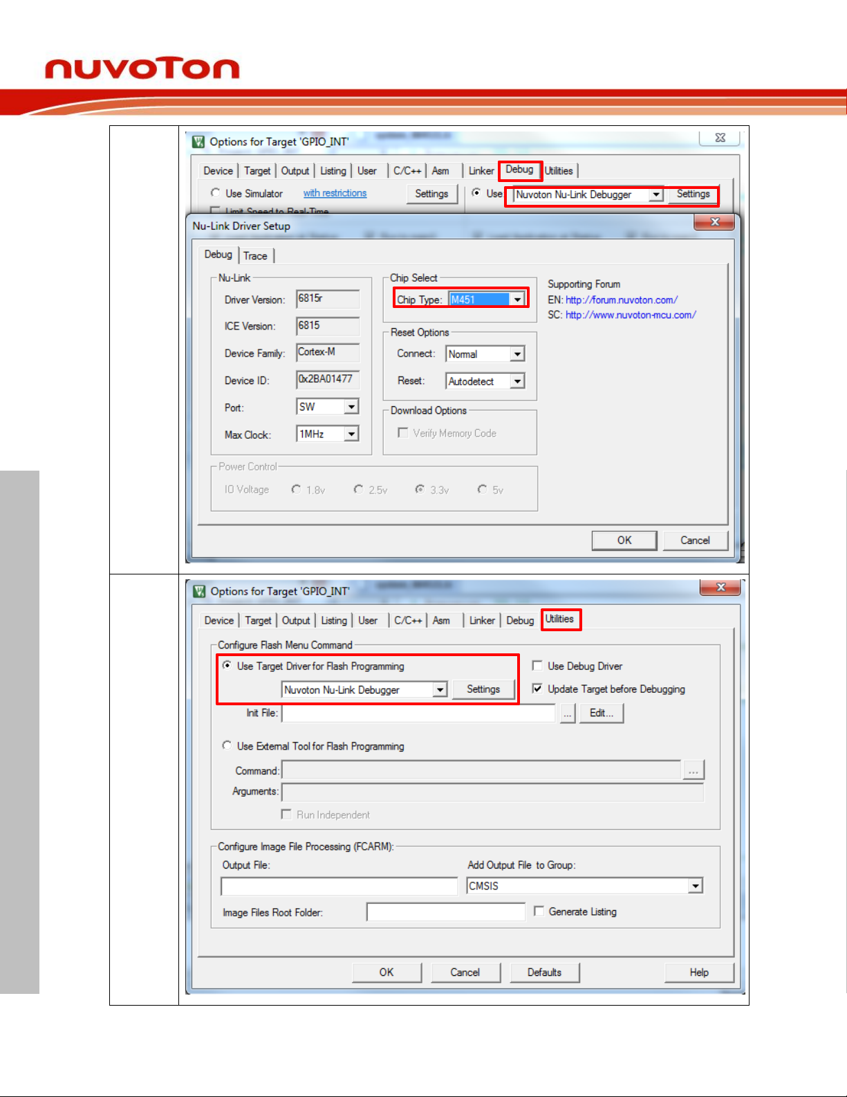
The target device has to be the same as the setting in Debug. Please click “Target Option” to
open the Option windows, and find the setting in “Device”, “Debug”, and “Utilities” page. Please
follow the steps below to check the setting.
M4521
Nov 28, 2018 Page 23 of 30 Rev 1.00
Page 24
M4521
NUTINY-SDK-M4521 USER MANUAL
Step 2
Step 3
Nov 28, 2018 Page 24 of 30 Rev 1.00
Page 25
NUTINY-SDK-M4521 USER MANUAL
5.3.3 Build and Download Code to NuTiny-SDK-M4521
Please build the project and download code to NuTiny-SDK-M4521.
5.3.4 Open the Serial Port Terminal
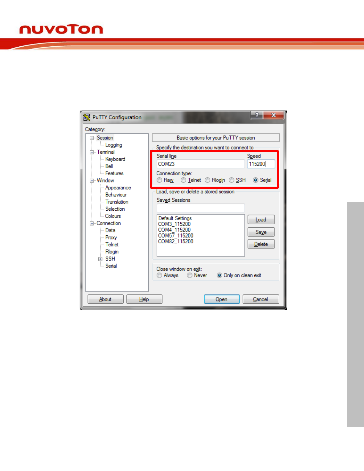
User can use serial port terminal, PuTTY for example, to print out debug message.
M4521
Figure 5-6 Set Baud Rate
5.3.5 Reset Chip
After pushing the reset button, the chip will reprogram application and print out debug message.
Nov 28, 2018 Page 25 of 30 Rev 1.00
Page 26
M4521
NUTINY-SDK-M4521 USER MANUAL
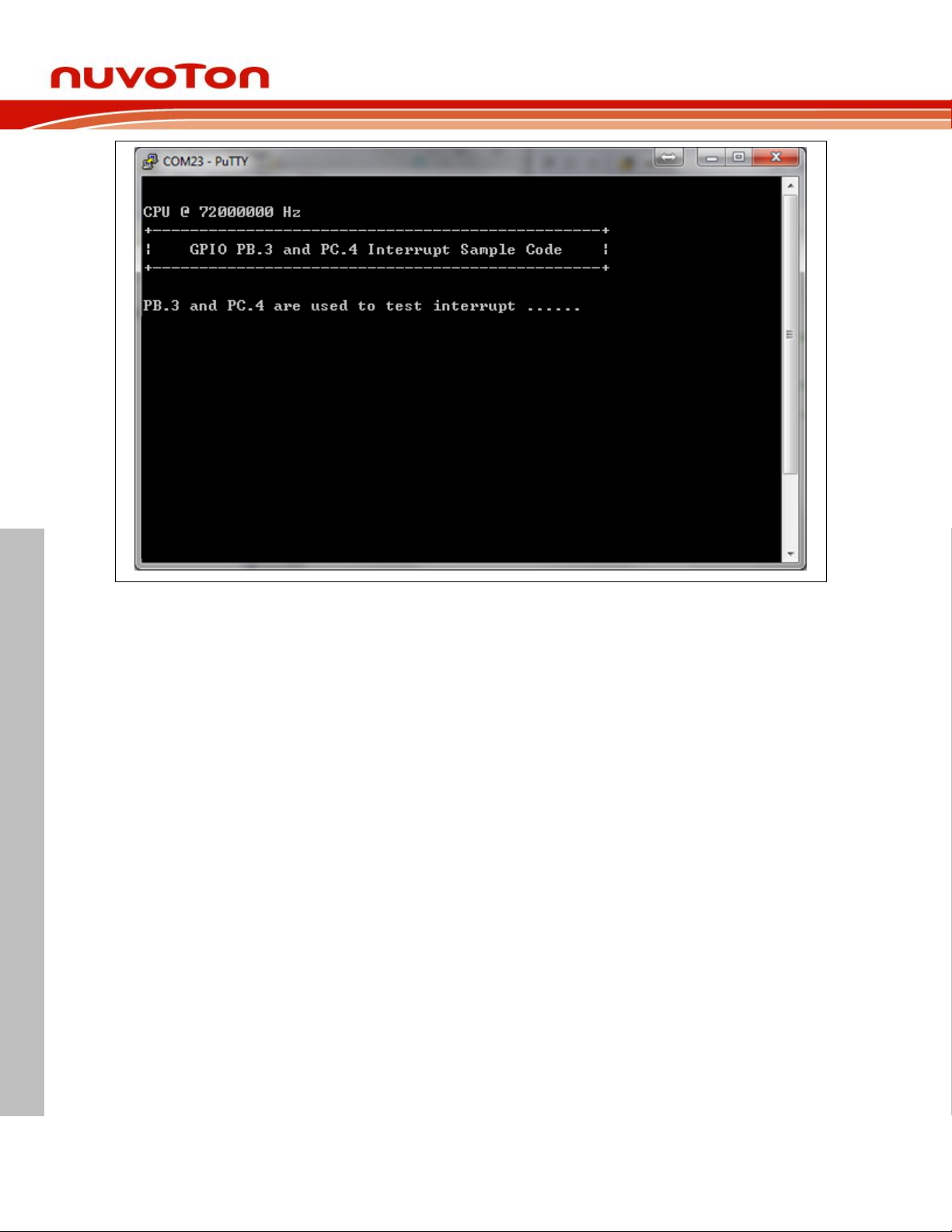
Figure 5-7 Serial Port Terminal Windows
Notice: Please switch SW2 on before the NuTiny-SDK-M4521 connects to the PC. When the NuTinySDK-M4521 connects to the PC with SW2 switch on, PC will detect VCOM as a USB device and the
detection will only be processed once. VCOM will not function if switch on SW2 after the connection.
Nov 28, 2018 Page 26 of 30 Rev 1.00
Page 27
NUTINY-SDK-M4521 USER MANUAL
6 NUTINY-SDK-M4521 SCHEMATIC
USB_PWR_EN P50
USB_OC# P49
1 2
D2
NC
RB060L
VDD
P20
1 2
D1
SS24A
RB060L
R14
0
R0603
C13
0.1u
C0603
USB_VBUS
D-
P19
D+
X2
12MHz SMD X3225B
XIN
1
GND
2
GND4XOUT
3
C9
20p
C0603
DX32O P14
C1
20p
C0603
ICERST P5
P18
P7
P8
P55
P54
P56
P53
USB_D+P46
USB_IDP47
P43
USB_D-P45
USB_VBUSP44
ICECLKP35
ICEDATP36
X1
X3215 32.768KHz SMD
ADAVSS
D12MOP22
P24
P26
LEDP27
D12MIP23
P25
R21
0
R0603
VDD
P17
P13
P33
D12MO
R7
0
R0603
ICETX
D12MI
R5
330
R0603
12
IO1
0805LED_Red
KP-2012
VDD
R2
0
R0603
LED
R6
0
R0603
DX32O
DX32I
P51
P34
ICERX
C3
10uF/10V
TANT-A
P52
R15
0
R0603
P37
C8
10uF/10V
TANT-A
Title
Size D ocument Num ber Rev
Date: Sheet of
1.1
NuTiny-EVB-M4521-LQFP64 V1.1
A3
Wednesday , Nov ember 28, 2018
C5
10uF/10V
TANT-A
C11
1u
C0603
P57
D+
D-
AVDD
VREF
1 2
POWER1
0805LED_Red
KP-2012
R4
330
R0603
VREF
C7
0.1u
C0603
P58
USB_ID
DD+
C21
0.1u
C0603
VDD
USB_OC#
C6
0.1u
C0603
R8
27
R0603
P38
CB1
0.1u
C0603
L3 L0603
U4
TPS2065CDBVR-2
OUT
1
GND
2
OC#
3
IN
5
EN/EN#
4
NCT3520U High Active
USB_D-
USB_D+
R10
27
R0603
J3
MICRO_USB_AB_LS
VBUS
1
D-
2
D+
3
GND
5
ID
4
Shield
6
Shield
7
Shield
8
Shield
9
+
CT1
1uF/6.3V
TANT-A
C4
0.1u
C0603
R22
NC
R0603
J1
NC
1
2
3
4
5
P59
U1
M4521SE6AE
PC.5
32
PC.4
31
PC.0
27
PC.1
28
PC.3
30
PC.2
29
LDO_CAP
26
VDD
25
VSS
24
PF.4/XT1_IN
23
PF.3/XT1_OUT
22
PD.7
21
PD.15
20
PD.14
19
PD.13
18
PD.12
17
PF.216X32I_PF.115X32O/PF.014PD.211PD.110PD.99PD.88VBAT
13
PB.63AVSS7PD.06PB.74nRESET5PD.3
12
PB.15
1
PB.11
63
PB.8
62
PB.4
61
PB.3
60
PB.2
59
PB.1
58
PB.12
64
PB.0
57
VREF
56
AVDD
55
VDD
54
VSS
53
PA.0
52
PA.1
51
PA.2
50
PA.3
49
USB_VDD33_CAP
48
PF.7/USB_I D
47
USB_D+
46
USB_D-
45
USB_VBUS
44
VDDIO
43
PE.1342PE.1241PE.1140PE.10
39
PE.938PE.8
37
PF.6/IC E_DAT
36
PF.5/IC LE_CLK
35
PC.734PC.6
33
PB.5
2
USB_ID
P1
P5
P3
P39
JP7
NC
1 2
3 4
5 6
7 8
9 10
11 12
13 14
15 16
JP8
NC
1 2
3 4
5 6
7 8
9 10
11 12
13 14
15 16
JP6
NC
1 2
3 4
5 6
7 8
9 10
11 12
13 14
15 16
P7
P9
P13
P11
JP5
NC
1 2
3 4
5 6
7 8
9 10
11 12
13 14
15 16
P15
P14
P16
P8
P12
P6
P10
P17
P31
P23
P2
P4
P25
P29
P19
P21
P27
P32
P24
P30
P20
P22
P47
P39
P33
P26
P28
P18
P36
P41
P45
P35
P37
P44
P48
P40
P34
P46
R23
NC
R0603
P51
P63
P55
P49
P42
P38
P62
P53
P59
P57
P61
P54
P60
P64
P56
P50
P43
P58
P52
P60
P40
R24
15k
R0603
P1
ICEDAT
ICERST
VDD
JP2
NC
1 2
3 4
5 6
7 8
9 10
ICECLK
VDD
R1
10K
R0603
ICERST
SW1
PUSH BOTTOM-4 Pin
SW4-SMD
R17
0
R0603
R25
15k
R0603
ICETX
ICERX
C10
20p
C0603
C2
20p
C0603
P61
JP1
NC
1
2
JP4
NC
1
2
P41
USB Host/Device
VCC5
Reset CrystalDebug Interface & Off Page
P62
P42
USB_VBUS
P32
NCT3520U pin3(OC#) is Open Drain Pin
P63
USB_OC#
R11
4.7K
R0603
VDD
VDD
ADAVSS
P2
AVDD
L1
L0603
P3
R20
0
R0603
P64
P48
P4
LED
DX32I P15
P6ICERX
Connector
P31
P9
R3
0
R0603
P30
Power
P10ICETX
TICEDAT
VDD
TICECLK
TICERST
R9
NC
R0603
VDD
USB_PWR_EN
P29
L2
L0603
C12
1u
C0603
P11
P28
P12
P21
P16
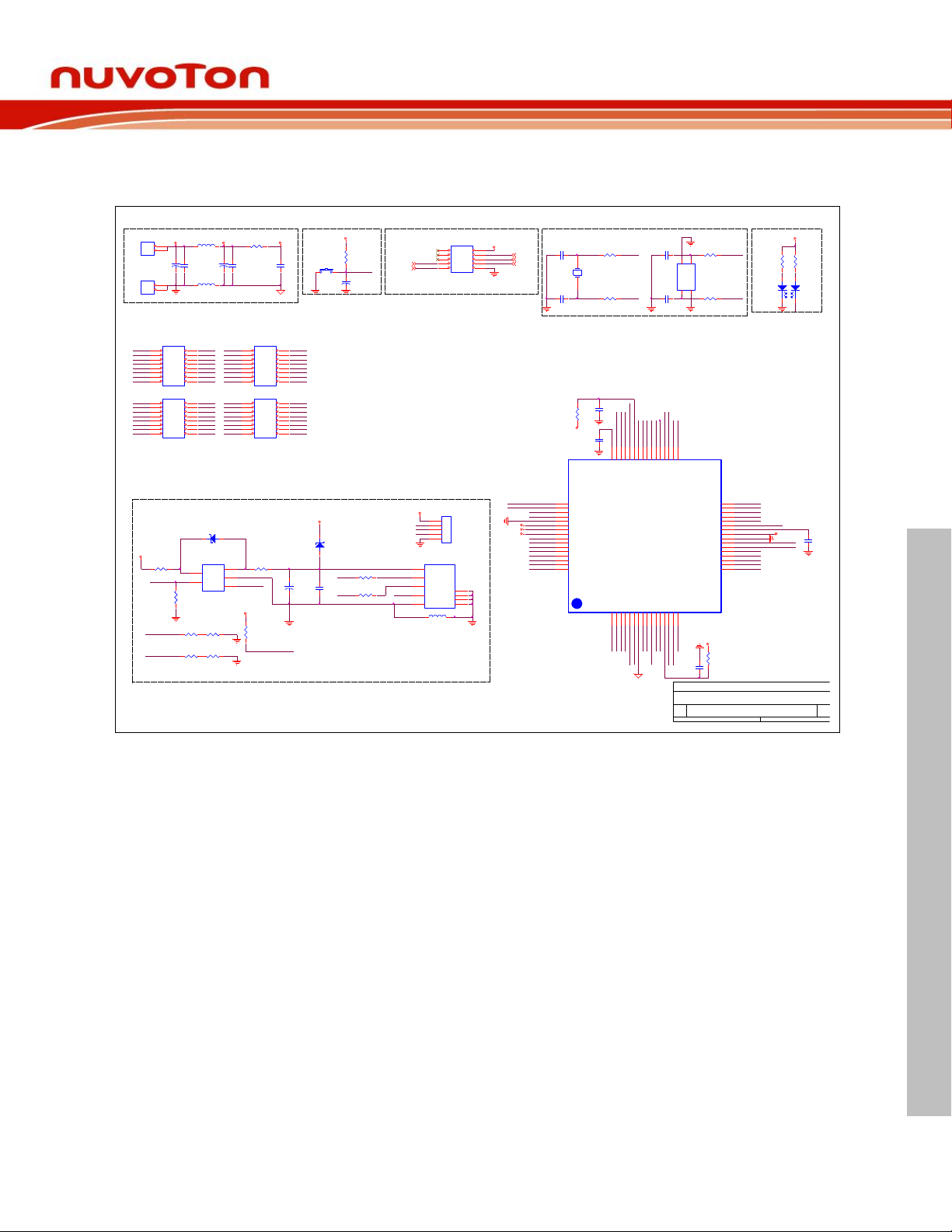
NuTiny-EVB-M4521 Schematic 6.1
M4521
Nov 28, 2018 Page 27 of 30 Rev 1.00
Page 28
M4521
NUTINY-SDK-M4521 USER MANUAL
Crystal
VCC5
X3
12MHz SMD X3225B
XIN
1
GND
2
GND4XOUT
3
USB Test Interface
12
IDLE1
0805LED_Red
KP-2012
ISPLED
RED
12
ICP1
0805LED_Orange
KP-2012
12
ICE1
0805LED_Red
KP-2012
ICELED
RP1
8P4R-330
8P4RA
1 2
3 4
5 6
7 8
12
BUSY1
0805LED_Green
KP-2012
GREEN
C15
20p
C0603
R18
27
R0603
R16
27
R0603
R13
NC
R0603
C14
20p
C0603
LED Display
GND
1 2 3 4
ON
SW2
HPS604-E
VCOM SW
DVBUS
VCOM_pin
TXD
RXD
RTDA333
RTDA40
VCC
VCC
VCC
VDD
C19
0.1u
C0603
R19
10K
R0603
VCC
TICEDAT
TICECLK
TICERST
Title
Size Doc ument N umber Rev
Date: Sheet of
3.0
NuLink-Me
A4
Friday , Oct ober 05, 2018
R12
27
R0603
12M_O
VCOM_pin
J2
MICRO_USB_AB_LS
VBUS
1
D-
2
D+
3
GND
5
ID
4
Shield
6
Shield
7
Shield
8
Shield
9
L5FERRITE BEAD
VCC
ICE_AVDD
ADAVSS
L6FERRITE BEAD
JP11
NC
1 2
3 4
5 6
7 8
9 10
TICECLK
TICEDAT
TICERST
JP13
NC
1
2
3
4
5
ICE_AVDD
ADAVSS
ICE_CLK
ICE_RST
ICE_DAT
RXD
TXD
ICERX
ICETX
DP
DM
SWD Interface & Off Page
DEBUG Interface
12M_I
TICEDAT
C20
10uF/10V
TANT-A
U3
NUC12SRE3DE
PA0/ADC0
44
PA1/ADC1
45
PA2/ADC2
46
PA3/ADC3
47
PA4/ADC4
48
INT0/PB14
1
CPO1/PB13
2
CPO0/PB12
3
VBUS17VDD3318D-19D+20PB0/RX021PB1/TX022PB2/RTS023PB3/CTS024PC2/SDI0026PC1/SPCLK027PC0/SS00
28
PC11/SDO10
33
PC10/SDI10
34
PC9/SPCLK1
35
PC8/SS10
36
PA15/PWM3
37
PA14/PWM2
38
PA13/PWM1
39
X32I
4
X32O
5
I2C1SCL/PA11
6
I2C0SDA/PA8
9
I2C1SDA/PA10
7
I2C0SCL/PA9
8
RX1/PB4
10
TX1/PB5
11
RTS1/PB6
12
CTS1/PB7
13
PC3/SDO00
25
AVSS
43
ICE_CK
42
ICE_DAT
41
PA12/PWM0
40
LDO
14
VSS
16
VDD
15
ADC/PA5
49
ADC6/PA650ADC7/PA7
51
AVDD
52
CPN0/PC7
53
CPP0/PC6
54
CPN1/PC15
55
CPP1/PC14
56
INT1/PB15
57
XT1_Out
58
XT1_In
59
/RESET
60
VSS1
61
VDD1
62
PVSS
63
STADC/TM0/PB8
64
PE529PB11/TM330PB10/SS01/TM231PB9/SS11/TM1
32
ICETX
JP12
NC
1
2
3
4
DM
DP
DVBUS
1 2
D3 SS24A
RB060L
ICERX
JPR1
SMD 1&2 (0R)
1
2
3
12M_I
ICE_RST
12M_O
C18
10uF/10V
TANT-A
ISPLED
RED
GREEN
C16
10uF/10V
TANT-A
VCC
ICELED
Power
ICERX
ICETX
CB2
0.1u
C0603
C17
0.1u
C0603
TICERST
RTCK1
100K
R0603
TICECLK
RTDA1
100K
R0603
RRSET1
100K
R0603
VCC
ICE_CLK
ICE_DAT
1 2
PD1
SS24A
RB060L
DVBUS
VCC
UP1
ACE1117C33XM+H
IN3GND1OUT2OUT
4
L4
L0603
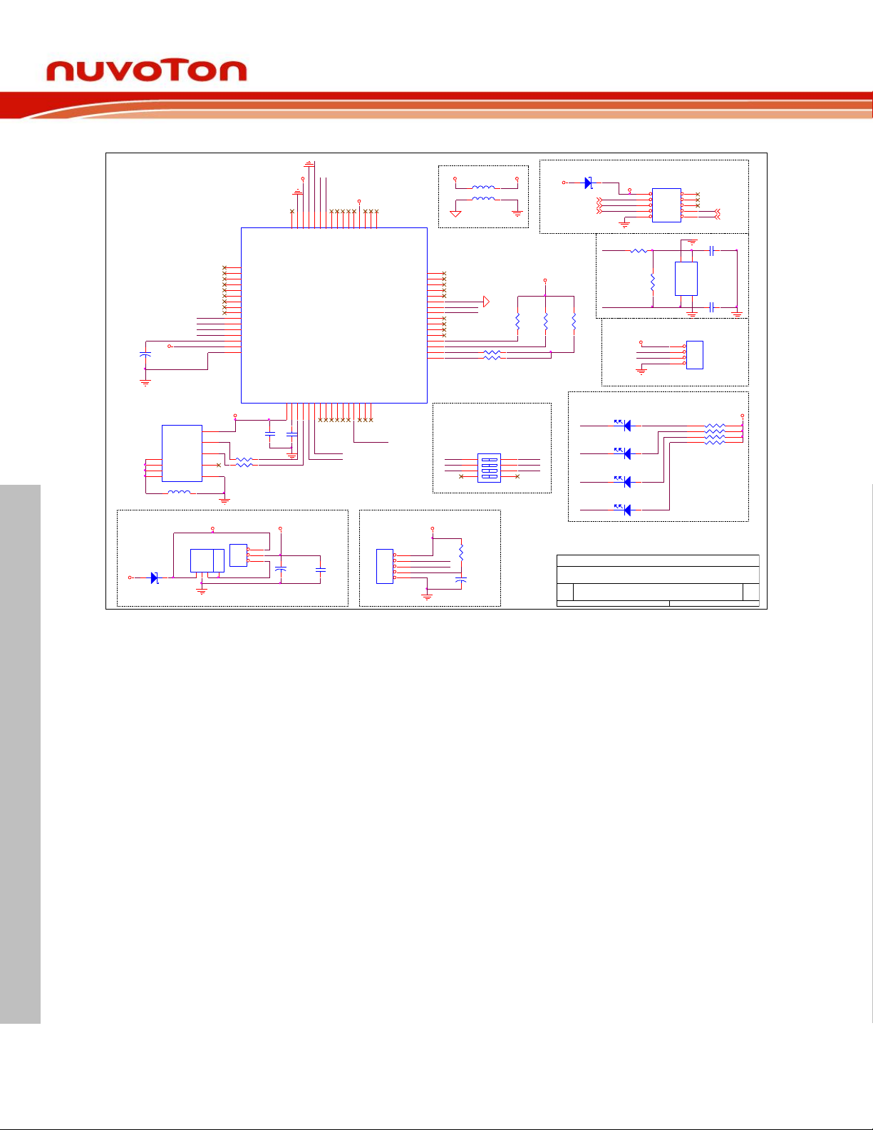
Nu-Link-Me V3.0 Schematic 6.2
Nov 28, 2018 Page 28 of 30 Rev 1.00
Page 29

NUTINY-SDK-M4521 USER MANUAL
7 REVISION HISTORY
Date
Revision
Description
2018.11.28
1.00
1. Initially issued.
M4521
Nov 28, 2018 Page 29 of 30 Rev 1.00
Page 30
M4521
NUTINY-SDK-M4521 USER MANUAL
Important Notice
Nuvoton Products are neither intended nor warranted for usage in systems or equipment, any
malfunction or failure of which may cause loss of human life, bodily injury or severe property
damage. Such applications are deemed, “Insecure Usage”.
Insecure usage includes, but is not limited to: equipment for surgical implementation, atomic
energy control instruments, airplane or spaceship instruments, the control or operation of
dynamic, brake or safety systems designed for vehicular use, traffic signal instruments, all
types of safety devices, and other applications intended to support or sustain life.
All Insecure Usage shall be made at customer’s risk, and in the event that third parties lay
claims to Nuvoton as a result of customer’s Insecure Usage, customer shall indemnify the
damages and liabilities thus incurred by Nuvoton.
Nov 28, 2018 Page 30 of 30 Rev 1.00
 Loading...