

NTE NTE5618, NTE5615, NTE5613, NTE5611 Datasheet

NTE5611 thru NTE5618
TRIAC – 10 Amp
Description:
The NTE5611 through NTE5618 TRIACs are designed primarily for full–wave AC control applications, such as light dimmers, motor controls, heating controls, and power supplies; or wherever full–
wave silicon gate controlled solid–state devices are needed. TRIAC type thyristors switch from a
blocking to a conducting state for either polarity of applied anode voltage with positive or negative gate
triggering.
Features:
D All Diffused and Passivated Junctions for Greater Parameter Uniformity and Stability
D Small, Rugged, Thermopad Construction for Low Thermal Resistance, High Heat Dissipation
and Durability.
D Gate Triggering Guaranteed in Four Modes
Absolute Maximum Ratings: (Note 1)
Repetitive Peak Off–State Voltage (TJ = +100°C, Note 2), V
NTE5611 25V. . . . . . . . . . . . . . . . . . . . . . . . . . . . . . . . . . . . . . . . . . . . . . . . . . . . . . . . . . . . . . . . . . . .
NTE5612 50V. . . . . . . . . . . . . . . . . . . . . . . . . . . . . . . . . . . . . . . . . . . . . . . . . . . . . . . . . . . . . . . . . . . .
NTE5613 100V. . . . . . . . . . . . . . . . . . . . . . . . . . . . . . . . . . . . . . . . . . . . . . . . . . . . . . . . . . . . . . . . . . .
NTE5615 300V. . . . . . . . . . . . . . . . . . . . . . . . . . . . . . . . . . . . . . . . . . . . . . . . . . . . . . . . . . . . . . . . . . .
NTE5618 600V. . . . . . . . . . . . . . . . . . . . . . . . . . . . . . . . . . . . . . . . . . . . . . . . . . . . . . . . . . . . . . . . . . .
On–State Current RMS (TC = +75°C), I
T(RMS)
Peak Surge Current (One Full Cycle, 60Hz, TJ = –40° to +100°C), I
Circuit Fusing Considerations (TJ = –40° to +100°C, t = 1.0 to 8.3ms), I2t 40A2s. . . . . . . . . . . . . . . .
Peak Gate Power, P
Average Gate Power, P
GM
0.5W. . . . . . . . . . . . . . . . . . . . . . . . . . . . . . . . . . . . . . . . . . . . . . . . . . . . . . .
G(AV)
Peak Gate Current, IGM 2A. . . . . . . . . . . . . . . . . . . . . . . . . . . . . . . . . . . . . . . . . . . . . . . . . . . . . . . . . . . . .
Operating Junction Temperature Range, TJ –40° to +100°C. . . . . . . . . . . . . . . . . . . . . . . . . . . . . . . . .
Storage Temperature Range, T
–40° to +150°C. . . . . . . . . . . . . . . . . . . . . . . . . . . . . . . . . . . . . . . . . .
stg
Mounting Torque (6–32 Screw, Note 3) 12in. lb.. . . . . . . . . . . . . . . . . . . . . . . . . . . . . . . . . . . . . . . . . . . .
Thermal Resistance, Junction–to–Case, R
Thermal Resistance, Case–to–Ambient, R
thJC
thJA
DRM
100A. . . . . . . . . . . . . . . . . .
TSM
10A. . . . . . . . . . . . . . . . . . . . . . . . . . . . . . . . . . . . . . . . . .
10W. . . . . . . . . . . . . . . . . . . . . . . . . . . . . . . . . . . . . . . . . . . . . . . . . . . . . . . . . . . .
2°C/W. . . . . . . . . . . . . . . . . . . . . . . . . . . . . . . . . . . . . . .
50°C/W. . . . . . . . . . . . . . . . . . . . . . . . . . . . . . . . . . . . . .
Note 1. NTE5618 is a discontinued device and no longer available.
Note 2. Ratings apply for open gate conditions. Thyristor devices shall not be tested with a constant
current source for blocking capability such that the voltage applied exceeds the rated blocking voltage.
Note 3. Torque rating applies with use of torque washer. Mounting torque in excess of 8 in. lbs. does
not appreciably lower case–to–sink thermal resistance. Anode lead and heatsink contact
pad are common.
Note 4. For soldering purposes (either terminal connection or device mounting), soldering tempera-
tures shall not exceed +230°C.
Electrical Characteristics: (TC = +25°C unless otherwise specified)
Parameter Symbol Min Typ Max Unit
Peak Blocking Current (Either Direction)
(Rated V
, TJ = 100°C, Gate Open)
DRM
On–State Voltage (Either Direction)
(I
= 14A Peak)
TM
Gate Trigger Current (Continuous DC)
(Main Terminal Voltage = 12V, R
MT
(+), G (+); MT2 (–), G (–)
2
MT
(+), G (–); MT2 (–), G (+)
2
= 100Ω)
L
Gate Trigger Voltage (Continuous DC)
(Main Terminal Voltage = 12V, R
MT
(+), G (+); MT2 (–), G (–)
2
MT
(+), G (–); MT2 (–), G (+)
2
= 100Ω)
L
Gate Trigger Voltage (Continuous DC – All Modes)
(Main Terminal Voltage = Rated V
, RL = 100Ω, TJ = +100°C)
DRM
Holding Current (Either Direction)
(Main Terminal Voltage = 12Vdc, Gate Open, I
Turn–On Time
(I
= 14A, IGT = 100mA)
TM
Blocking Voltage Application Rate at Commutation
(At V
, TJ = +75°C, Gate Open)
DRM
= 100mA)
T
I
DRM
V
TM
I
GT
V
GT
V
GD
I
H
t
on
dv/dt
– – 2
– 1.3 1.8
–
–
–
–
–
–
0.9
1.0
50
75
2.0
2.5
0.2 – –
– – 50
– 1.5 –
– 5 –
mA
V
mA
V
V
mA
µs
V/µs
.668
(17.0)
Max
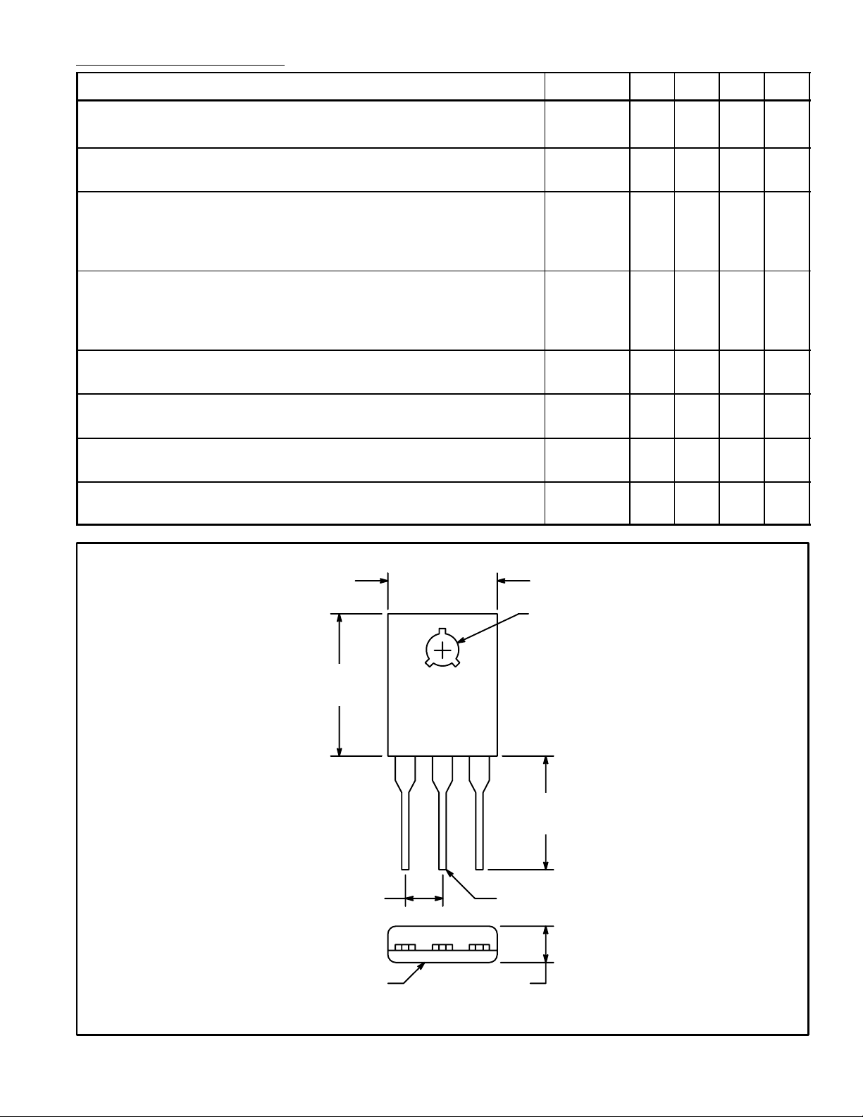
Heat Sink Contact
Area (Bottom)
.166 (4.23)
.530 (13.4) Max
MT
1
.150 (3.82) Max
.143 (3.65) Dia Thru
Gate
.655
(16.6)
Max
MT2 (Heat Sink Area)
 Loading...