

NTE NTE56068 Datasheet

NTE56068 & NTE56069
TRIAC, 16A, High Commutation
Description:
The NTE56068 and NTE56069 are glass passivated, high commutation TRIACs in an isolated full–
pack type package designed for use in circuits where high static and dynamic dV/dt and high dI/dt
can occur. These devices will commutate the full rated RMS current at the maximum rated junction
temperature, without the aid of a snubber.
Absolute Maximum Ratings:
Repetitive Peak Off–Sate Voltage (Note 1), V
NTE56068 600V. . . . . . . . . . . . . . . . . . . . . . . . . . . . . . . . . . . . . . . . . . . . . . . . . . . . . . . . . . . . . . . . .
NTE56069 800V. . . . . . . . . . . . . . . . . . . . . . . . . . . . . . . . . . . . . . . . . . . . . . . . . . . . . . . . . . . . . . . . .
RMS On–State Current (Full Sine Wave, THS ≤ 38°C), IT(RMS) 16A. . . . . . . . . . . . . . . . . . . . . . . . . .
Non–Repetitive Peak On–State Current, I
(Full Sine Wave, TJ = +25°C prior to Surge)
t = 20ms 140A. . . . . . . . . . . . . . . . . . . . . . . . . . . . . . . . . . . . . . . . . . . . . . . . . . . . . . . . . . . . . . . .
t = 16.7ms 150A. . . . . . . . . . . . . . . . . . . . . . . . . . . . . . . . . . . . . . . . . . . . . . . . . . . . . . . . . . . . . . .
I2t for Fusing (t = 10ms), I2t 98A2sec. . . . . . . . . . . . . . . . . . . . . . . . . . . . . . . . . . . . . . . . . . . . . . . . . . . . . .
Repetitive Rate–of–Rise of On–State Current after Triggering, dIT/dt
(ITM = 20A, IG = 0.2A, dIG/dt = 0.2A/µs) 100A/µs. . . . . . . . . . . . . . . . . . . . . . . . . . . . . . . . . . . . .
Peak Gate Current, I
Peak Gate Voltage, V
Peak Gate Power, P
GM
GM
GM
Average Gate Power (Over Any 20ms Period), P
Operating Junction Temperature, T
Storage Temperature Range, T
J
stg
Thermal Resistance, Junction–to–Heatsink (Full or Half Cycle), R
With Heatsink Compound 4.0K/W. . . . . . . . . . . . . . . . . . . . . . . . . . . . . . . . . . . . . . . . . . . . . . . . . .
Without Heatsink Compound 5.5K/W. . . . . . . . . . . . . . . . . . . . . . . . . . . . . . . . . . . . . . . . . . . . . . .
Typical Thermal Resistance, Junction–to–Ambient, R
TSM
DRM
G(AV)
thJA
2A. . . . . . . . . . . . . . . . . . . . . . . . . . . . . . . . . . . . . . . . . . . . . . . . . . . . . . . . . . . . . .
5V. . . . . . . . . . . . . . . . . . . . . . . . . . . . . . . . . . . . . . . . . . . . . . . . . . . . . . . . . . . . .
5W. . . . . . . . . . . . . . . . . . . . . . . . . . . . . . . . . . . . . . . . . . . . . . . . . . . . . . . . . . . . .
500mW. . . . . . . . . . . . . . . . . . . . . . . . . . . . . . . .
+125°C. . . . . . . . . . . . . . . . . . . . . . . . . . . . . . . . . . . . . . . . . . . . . . .
–40° to +150°C. . . . . . . . . . . . . . . . . . . . . . . . . . . . . . . . . . . . . . . . . .
thJHS
55K/W. . . . . . . . . . . . . . . . . . . . . . . . . . . . .
Note 1. Although not recommended, off–state voltages up to 800V may be applied without damage,
but the TRIAC may switch to the on–state. The rate–of–rise of current should not exceed
15A/µs.
Electrical Characteristics: (TJ = +25°C unless otherwise specfied)
Parameter Symbol Test Conditions Min Typ Max Unit
Static Characteristics
Gate Trigger Current
(+), G (+) I
MT
2
GT
MT2 (+), G (–) 2 21 50 mA
MT2 (–), G (–) 2 34 50 mA
Latching Current
MT2 (+), G (+) I
MT2 (+), G (–) – 34 90 mA
MT2 (–), G (–) – 30 60 mA
Holding Current I
On–State Voltage V
Gate Trigger Voltage V
Off–State Leakage Current I
Dynamic Characteristics
Critical Rate–of–Rise of
dVD/dt VDM = 67% V
Off–State Voltage
Critical Rate–of–Change of
dI
com
Commutating Current
Gate Controlled Turn–On Time t
Isolation Characteristics
RMS Isolation Voltage from All
V
ISOL
3 Pins to External Heatsink
Capacitance from T2 to
C
ISOL
External Heatsink
VD = 12V, IT = 0.1A, Note 2 2 18 50 mA
VD = 12V, IT = 0.1A – 31 60 mA
L
VD = 12V, IT = 0.1A – 31 60 mA
H
IT = 20A – 1.2 1.5 V
T
VD = 12V, IT = 0.1A – 0.7 1.5 V
GT
VD = 400V, IT = 0.1A, TJ = +125°C 0.25 0.4 – V
VD = V
D
max, TJ = +125°C – 0.1 0.5 mA
DRM
max, TJ = +125°C,
DRM
1000 4000 – V/µs
Exponential Waveform, Gate Open
/dt VDM = 400V, TJ = +1 25°C, ITRM S = 16A,
– 28 – A/ms
without Snubber, Gate Open
ITM = 20A, VD = V
gt
max, IG = 0.1A,
DRM
– 2 – µs
dIG/dt = 5A/µs
f = 50 – 60Hz, Sinusoidal Waveform,
– – 2500 V
R.H. ≤ 65%, Clean and Dustfree
f = 1MHz – 10 – pF
Note 2. Device does not trigger in the MT2 (–), G (+) quadrant.
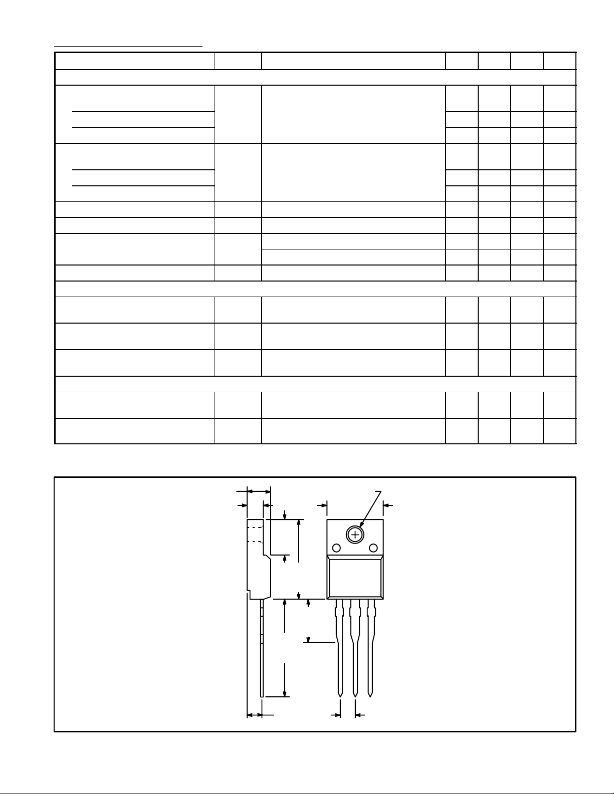
.181 (4.6) Max
.114 (2.9)
(13.5)
.126 (3.2) Dia Max
.252
(6.4)
.622
(15.0)
Max
.118
(3.0)
Max
.531
Min
.405 (10.3)
Isol
MT
1
Max
MT
2
G
.100 (2.54).098 (2.5)
 Loading...