

NTE NTE56060, NTE56058 Datasheet

NTE56058 thru NTE56060
TRIAC, 16A
Description:
The N TE56058 t hrough N TE56060 a re g lass p assivated T RIACs i n a n i solated f ull–pack t ype package
designed f or u se in a pplications r equiring h igh b idirectional t ransient a nd b locking v oltage c apability a nd
high thermal cycling performance. Typical applications include motor control, industrial and domestic
lighting, heating and static switching.
Absolute Maximum Ratings:
Repetitive Peak Off–Sate Voltage, V
NTE56058 (Note 1) 500V. . . . . . . . . . . . . . . . . . . . . . . . . . . . . . . . . . . . . . . . . . . . . . . . . . . . . . . . . .
NTE56059 (Note 1) 600V. . . . . . . . . . . . . . . . . . . . . . . . . . . . . . . . . . . . . . . . . . . . . . . . . . . . . . . . . .
NTE56060 800V. . . . . . . . . . . . . . . . . . . . . . . . . . . . . . . . . . . . . . . . . . . . . . . . . . . . . . . . . . . . . . . . .
RMS On–State Current (Full Sine Wave, THS ≤ 38°C), IT(RMS) 16A. . . . . . . . . . . . . . . . . . . . . . . . . .
Non–Repetitive Peak On–State Current, I
(Full Sine Wave, TJ = +125°C prior to Surge, with Reapplied V
t = 20ms 140A. . . . . . . . . . . . . . . . . . . . . . . . . . . . . . . . . . . . . . . . . . . . . . . . . . . . . . . . . . . . . . . .
t = 16.7ms 150A. . . . . . . . . . . . . . . . . . . . . . . . . . . . . . . . . . . . . . . . . . . . . . . . . . . . . . . . . . . . . . .
I2t for Fusing (t = 10ms), I2t 98A2sec. . . . . . . . . . . . . . . . . . . . . . . . . . . . . . . . . . . . . . . . . . . . . . . . . . . . . .
Repetitive Rate–of–Rise of On–State Current after Triggering, dIT/dt
(ITM = 20A, IG = 0.2A, dIG/dt = 0.2A/µs)
MT2 (+), G (+) 50A/µs. . . . . . . . . . . . . . . . . . . . . . . . . . . . . . . . . . . . . . . . . . . . . . . . . . . . . . . . .
MT2 (+), G (–) 50A/µs. . . . . . . . . . . . . . . . . . . . . . . . . . . . . . . . . . . . . . . . . . . . . . . . . . . . . . . . . .
MT2 (–), G (–) 50A/µs. . . . . . . . . . . . . . . . . . . . . . . . . . . . . . . . . . . . . . . . . . . . . . . . . . . . . . . . . .
MT2 (–), G (+) 10A/µs. . . . . . . . . . . . . . . . . . . . . . . . . . . . . . . . . . . . . . . . . . . . . . . . . . . . . . . . . .
Peak Gate Current, I
Peak Gate Voltage, V
Peak Gate Power, P
GM
GM
GM
Average Gate Power (Over Any 20ms Period), P
Operating Junction Temperature, T
Storage Temperature Range, T
Thermal Resistance, Junction–to–Heatsink (Full or Half Cycle), R
With Heatsink Compound 4.0K/W. . . . . . . . . . . . . . . . . . . . . . . . . . . . . . . . . . . . . . . . . . . . . . . . . .
Without Heatsink Compound 5.5K/W. . . . . . . . . . . . . . . . . . . . . . . . . . . . . . . . . . . . . . . . . . . . . . .
Typical Thermal Resistance, Junction–to–Ambient, R
stg
J
DRM
TSM
G(AV)
thJA
thJHS
DRM
max)
2A. . . . . . . . . . . . . . . . . . . . . . . . . . . . . . . . . . . . . . . . . . . . . . . . . . . . . . . . . . . . . .
5V. . . . . . . . . . . . . . . . . . . . . . . . . . . . . . . . . . . . . . . . . . . . . . . . . . . . . . . . . . . . .
5W. . . . . . . . . . . . . . . . . . . . . . . . . . . . . . . . . . . . . . . . . . . . . . . . . . . . . . . . . . . . .
500mW. . . . . . . . . . . . . . . . . . . . . . . . . . . . . . . .
+125°C. . . . . . . . . . . . . . . . . . . . . . . . . . . . . . . . . . . . . . . . . . . . . . .
–40° to +150°C. . . . . . . . . . . . . . . . . . . . . . . . . . . . . . . . . . . . . . . . . .
55K/W. . . . . . . . . . . . . . . . . . . . . . . . . . . . .
Note 1. Although not recommended, off–state voltages up to 800V may be applied without damage,
but the TRIAC may switch to the on–state. The rate–of–rise of current should not exceed
15A/µs.
Electrical Characteristics: (TJ = +25°C unless otherwise specfied)
Parameter Symbol Test Conditions Min Typ Max Unit
Static Characteristics
Gate Trigger Current
(+), G (+) I
MT
2
GT
MT2 (+), G (–) – 8 35 mA
MT2 (–), G (–) – 10 35 mA
MT2 (–), G (+) – 22 70 mA
Latching Current
MT2 (+), G (+) I
MT2 (+), G (–) – 20 60 mA
MT2 (–), G (–) – 8 40 mA
MT2 (–), G (+) – 10 60 mA
Holding Current I
On–State Voltage V
Gate Trigger Voltage V
Off–State Leakage Current I
Dynamic Characteristics
Critical Rate–of–Rise of
dVD/dt VDM = 67% V
Off–State Voltage
Critical Rate–of–Change of
dV
com
Commutating Voltage
Gate Controlled Turn–On Time t
Isolation Characteristics
RMS Isolation Voltage from All
V
ISOL
3 Pins to External Heatsink
Capacitance from T2 to
C
ISOL
External Heatsink
VD = 12V, IT = 0.1A – 5 35 mA
VD = 12V, IT = 0.1A – 7 40 mA
L
VD = 12V, IT = 0.1A – 6 30 mA
H
IT = 20A – 1.2 1.6 V
T
VD = 12V, IT = 0.1A – 0.7 1.5 V
GT
VD = 400V, IT = 0.1A, TJ = +125°C 0.25 0.4 – V
VD = V
D
max, TJ = +125°C – 0.1 0.5 mA
DRM
max, TJ = +125°C,
DRM
100 250 – V/µs
Exponential Waveform, Gate Open
/dt VDM = 400V, TJ = +95°C, ITRMS = 16A,
dI
/dt = 7.2A/ms, Gate Open
com
ITM = 20A, VD = V
gt
max, IG = 0.1A,
DRM
– 20 – V/µs
– 2 – µs
dIG/dt = 5A/µs
R.H. ≤ 65%, Clean and Dustfree – – 1500 V
f = 1MHz – 12 – pF
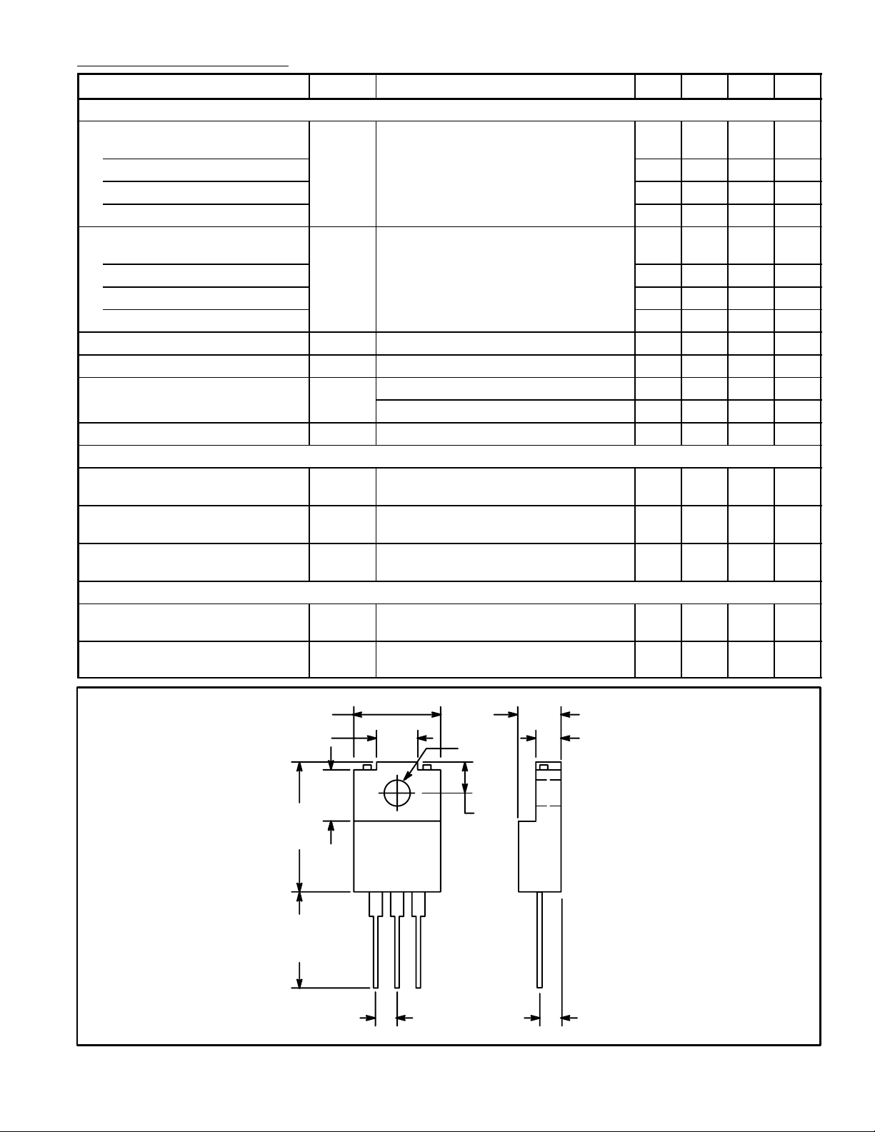
.402 (10.2) Max
.224 (5.7) Max
.295
(7.5)
.669
(17.0)
Max
MT1MT2G
.531
(13.5)
Min
.100 (2.54) .059 (1.5) Max
.122 (3.1)
Dia
.165
(4.2)
.173 (4.4)
Max
.114 (2.9)
Max
 Loading...