

NTE NTE56049 Datasheet

NTE56049 & NTE56050
TRIAC, 4A Low Logic Level
Description:
The NTE56049 and NTE56050 are glass passivated, Low Logic Level TRIACs in a TO220 type package designed for use in general purpose bidirectional switching and phase control applications.
These devices are intended to be interfaced directly to microcontrollers, logic integrated circuits, and
other low power gate trigger circuits.
Absolute Maximum Ratings:
Repetitive Peak Off–Sate Voltage (Note 1), V
NTE56049 500V. . . . . . . . . . . . . . . . . . . . . . . . . . . . . . . . . . . . . . . . . . . . . . . . . . . . . . . . . . . . . . . . .
NTE56050 600V. . . . . . . . . . . . . . . . . . . . . . . . . . . . . . . . . . . . . . . . . . . . . . . . . . . . . . . . . . . . . . . . .
RMS On–State Current (Full Sine Wave, TMB ≤ 107°C), IT(RMS) 4A. . . . . . . . . . . . . . . . . . . . . . . . . .
Non–Repetitive Peak On–State Current, I
(Full Sine Wave, TJ = +125°C prior to Surge, with Reapplied V
t = 20ms 25A. . . . . . . . . . . . . . . . . . . . . . . . . . . . . . . . . . . . . . . . . . . . . . . . . . . . . . . . . . . . . . . . .
t = 16.7ms 27A. . . . . . . . . . . . . . . . . . . . . . . . . . . . . . . . . . . . . . . . . . . . . . . . . . . . . . . . . . . . . . . .
I2t for Fusing (t = 10ms), I2t 3.1A2sec. . . . . . . . . . . . . . . . . . . . . . . . . . . . . . . . . . . . . . . . . . . . . . . . . . . . .
Repetitive Rate–of–Rise of On–State Current after Triggering, dIT/dt
(ITM = 6A, IG = 0.2A, dIG/dt = 0.2A/µs)
MT2 (+), G (+) 50A/µs. . . . . . . . . . . . . . . . . . . . . . . . . . . . . . . . . . . . . . . . . . . . . . . . . . . . . . . . .
MT2 (+), G (–) 50A/µs. . . . . . . . . . . . . . . . . . . . . . . . . . . . . . . . . . . . . . . . . . . . . . . . . . . . . . . . . .
MT2 (–), G (–) 50A/µs. . . . . . . . . . . . . . . . . . . . . . . . . . . . . . . . . . . . . . . . . . . . . . . . . . . . . . . . . .
MT2 (–), G (+) 10A/µs. . . . . . . . . . . . . . . . . . . . . . . . . . . . . . . . . . . . . . . . . . . . . . . . . . . . . . . . . .
Peak Gate Current, I
Peak Gate Voltage, V
Peak Gate Power, P
GM
GM
GM
Average Gate Power (Over Any 20ms Period), P
Operating Junction Temperature, T
Storage Temperature Range, T
J
stg
Thermal Resistance, Junction–to–Mounting Base, R
Full Cycle 3.0K/W. . . . . . . . . . . . . . . . . . . . . . . . . . . . . . . . . . . . . . . . . . . . . . . . . . . . . . . . . . . . . . . .
Half Cycle 3.7K/W. . . . . . . . . . . . . . . . . . . . . . . . . . . . . . . . . . . . . . . . . . . . . . . . . . . . . . . . . . . . . . . .
Typical Thermal Resistance, Junction–to–Ambient, R
TSM
DRM
G(AV)
thJMB
thJA
DRM
max)
2A. . . . . . . . . . . . . . . . . . . . . . . . . . . . . . . . . . . . . . . . . . . . . . . . . . . . . . . . . . . . . .
5V. . . . . . . . . . . . . . . . . . . . . . . . . . . . . . . . . . . . . . . . . . . . . . . . . . . . . . . . . . . . .
5W. . . . . . . . . . . . . . . . . . . . . . . . . . . . . . . . . . . . . . . . . . . . . . . . . . . . . . . . . . . . .
500mW. . . . . . . . . . . . . . . . . . . . . . . . . . . . . . . .
+125°C. . . . . . . . . . . . . . . . . . . . . . . . . . . . . . . . . . . . . . . . . . . . . . .
–40° to +150°C. . . . . . . . . . . . . . . . . . . . . . . . . . . . . . . . . . . . . . . . . .
60K/W. . . . . . . . . . . . . . . . . . . . . . . . . . . . .
Note 1. Although not recommended, off–state voltages up to 800V may be applied without damage,
but the TRIAC may switch to the on–State. The rate–of–rise of current should not exceed
3A/µs.
Electrical Characteristics: (TJ = +25°C unless otherwise specfied)
Parameter Symbol Test Conditions Min Typ Max Unit
Static Characteristics
Gate Trigger Current
MT2 (+), G (+) I
GT
MT2 (+), G (–) – 2.5 5 mA
MT2 (–), G (–) – 2.5 5 mA
MT2 (–), G (+) – 5 10 mA
Latching Current
MT2 (+), G (+) I
MT2 (+), G (–) – 4.5 15 mA
MT2 (–), G (–) – 1.2 10 mA
MT2 (–), G (+) – 2.2 15 mA
VD = 12V, IT = 0.1A – 2.0 5 mA
VD = 12V, IT = 0.1A – 1.6 10 mA
L
Holding Current I
On–State Voltage V
Gate Trigger Voltage V
Off–State Leakage Current I
Dynamic Characteristics
Critical Rate–of–Rise of
dVD/dt VDM = 67% V
Off–State Voltage
Gate Controlled Turn–On Time t
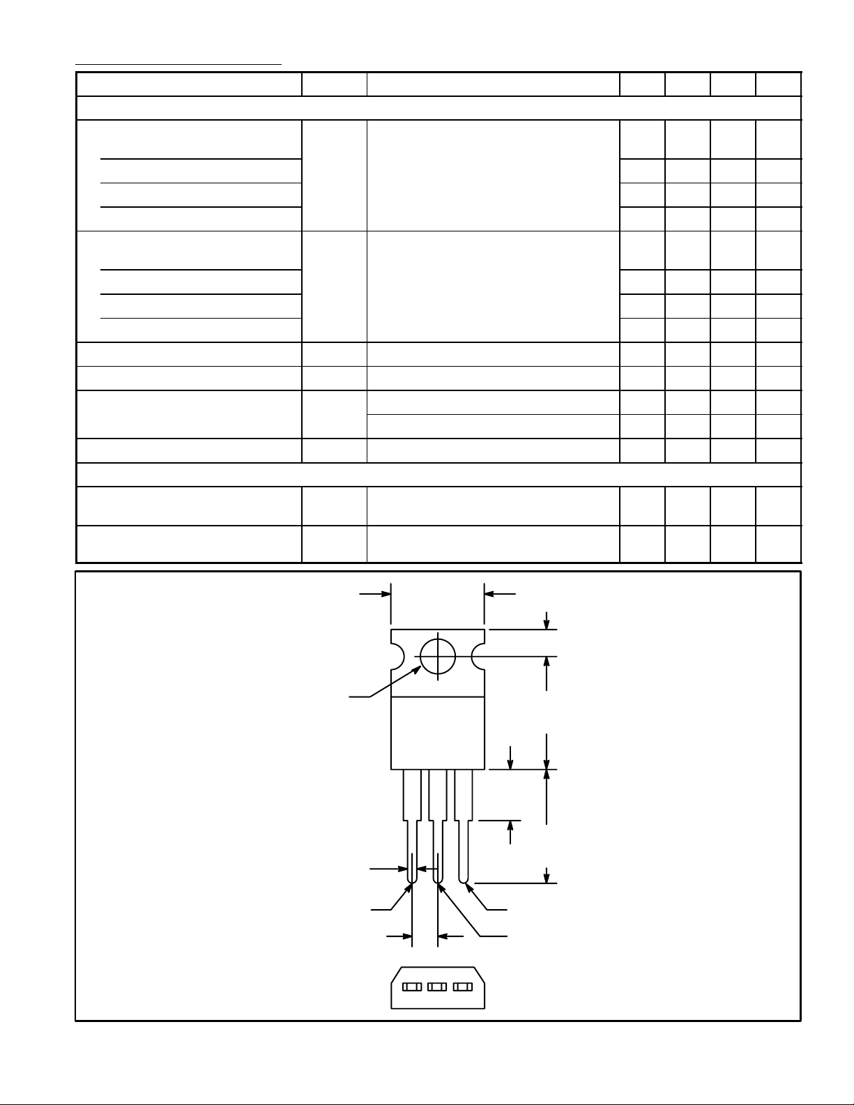
.147 (3.75)
Dia Max
VD = 12V, IT = 0.1A – 1.2 10 mA
H
IT = 5A – 1.4 1.7 V
T
VD = 12V, IT = 0.1A – 0.7 1.5 V
GT
VD = 400V, IT = 0.1A, TJ = +125°C 0.25 0.4 – V
VD = V
D
max, TJ = +125°C – 0.1 0.5 mA
DRM
max, TJ = +125°C,
DRM
– 5 – V/µs
Exponential Waveform, RGK = 1kΩ
ITM = 6A, VD = V
gt
max, IG = 0.1A,
DRM
– 2 – µs
dIG/dt = 5A/µs
.420 (10.67)
Max
.110 (2.79)
MT
2
.500
(12.7)
Max
.070 (1.78) Max
MT
.100 (2.54)
.250 (6.35)
Max
.500
(12.7)
Min
1
Gate
MT
2
 Loading...