

NTE NTE56047, NTE56046, NTE56045 Datasheet

NTE56045 thru NTE56047
TRIAC, 16A, Sensitive Gate
Description:
The N TE56045 through N TE56047 are g lass passivated, s ensi tive g ate TRIACs in a n i s olated full–
pack type package designed for use in general purpose bidirectional switching and phase control
applications, where high sensitivity is required in all four quadrants.
Absolute Maximum Ratings:
Repetitive Peak Off–Sate Voltage, V
DRM
NTE56045 (Note 1) 500V. . . . . . . . . . . . . . . . . . . . . . . . . . . . . . . . . . . . . . . . . . . . . . . . . . . . . . . . . .
NTE56046 (Note 1) 600V. . . . . . . . . . . . . . . . . . . . . . . . . . . . . . . . . . . . . . . . . . . . . . . . . . . . . . . . . .
NTE56047 800V. . . . . . . . . . . . . . . . . . . . . . . . . . . . . . . . . . . . . . . . . . . . . . . . . . . . . . . . . . . . . . . . .
RMS On–State Current (Full Sine Wave, THS ≤ 38°C), IT(RMS) 16A. . . . . . . . . . . . . . . . . . . . . . . . . .
Non–Repetitive Peak On–State Current, I
TSM
(Full Sine Wave, TJ = +125°C prior to Surge, with Reapplied V
DRM
max)
t = 20ms 140A. . . . . . . . . . . . . . . . . . . . . . . . . . . . . . . . . . . . . . . . . . . . . . . . . . . . . . . . . . . . . . . .
t = 16.7ms 150A. . . . . . . . . . . . . . . . . . . . . . . . . . . . . . . . . . . . . . . . . . . . . . . . . . . . . . . . . . . . . . .
I2t for Fusing (t = 10ms), I2t 98A2sec. . . . . . . . . . . . . . . . . . . . . . . . . . . . . . . . . . . . . . . . . . . . . . . . . . . . . .
Repetitive Rate–of–Rise of On–State Current after Triggering, dIT/dt
(ITM = 20A, IG = 0.2A, dIG/dt = 0.2A/µs)
MT2 (+), G (+) 50A/µs. . . . . . . . . . . . . . . . . . . . . . . . . . . . . . . . . . . . . . . . . . . . . . . . . . . . . . . . .
MT2 (+), G (–) 50A/µs. . . . . . . . . . . . . . . . . . . . . . . . . . . . . . . . . . . . . . . . . . . . . . . . . . . . . . . . . .
MT2 (–), G (–) 50A/µs. . . . . . . . . . . . . . . . . . . . . . . . . . . . . . . . . . . . . . . . . . . . . . . . . . . . . . . . . .
MT2 (–), G (+) 10A/µs. . . . . . . . . . . . . . . . . . . . . . . . . . . . . . . . . . . . . . . . . . . . . . . . . . . . . . . . . .
Peak Gate Current, I
GM
2A. . . . . . . . . . . . . . . . . . . . . . . . . . . . . . . . . . . . . . . . . . . . . . . . . . . . . . . . . . . . . .
Peak Gate Voltage, V
GM
5V. . . . . . . . . . . . . . . . . . . . . . . . . . . . . . . . . . . . . . . . . . . . . . . . . . . . . . . . . . . . .
Peak Gate Power, P
GM
5W. . . . . . . . . . . . . . . . . . . . . . . . . . . . . . . . . . . . . . . . . . . . . . . . . . . . . . . . . . . . .
Average Gate Power (Over Any 20ms Period), P
G(AV)
500mW. . . . . . . . . . . . . . . . . . . . . . . . . . . . . . . .
Operating Junction Temperature, T
J
+125°C. . . . . . . . . . . . . . . . . . . . . . . . . . . . . . . . . . . . . . . . . . . . . . .
Storage Temperature Range, T
stg
–40° to +150°C. . . . . . . . . . . . . . . . . . . . . . . . . . . . . . . . . . . . . . . . . .
Thermal Resistance, Junction–to–Heatsink (Full or Half Cycle), R
thJHS
With Heatsink Compound 4.0K/W. . . . . . . . . . . . . . . . . . . . . . . . . . . . . . . . . . . . . . . . . . . . . . . . . .
Without Heatsink Compound 5.5K/W. . . . . . . . . . . . . . . . . . . . . . . . . . . . . . . . . . . . . . . . . . . . . . .
Typical Thermal Resistance, Junction–to–Ambient, R
thJA
55K/W. . . . . . . . . . . . . . . . . . . . . . . . . . . . .
Note 1. Although not recommended, off–state voltages up to 800V may be applied without damage,
but the TRIAC may switch to the on–state. The rate–of–rise of current should not exceed
15A/µs.
Electrical Characteristics: (TJ = +25°C unless otherwise specfied)
Parameter Symbol Test Conditions Min Typ Max Unit
Static Characteristics
Gate Trigger Current
MT
2
(+), G (+) I
GT
VD = 12V, IT = 0.1A – 2.5 10 mA
MT2 (+), G (–) – 4.0 10 mA
MT2 (–), G (–) – 5.0 10 mA
MT2 (–), G (+) – 11 25 mA
Latching Current
MT2 (+), G (+) I
L
VD = 12V, IT = 0.1A – 3.2 30 mA
MT2 (+), G (–) – 16 40 mA
MT2 (–), G (–) – 4.0 30 mA
MT2 (–), G (+) – 5.5 40 mA
Holding Current I
H
VD = 12V, IT = 0.1A – 4.0 30 mA
On–State Voltage V
T
IT = 20A – 1.2 1.6 V
Gate Trigger Voltage V
GT
VD = 12V, IT = 0.1A – 0.7 1.5 V
VD = 400V, IT = 0.1A, TJ = +125°C 0.25 0.4 – V
Off–State Leakage Current I
D
VD = V
DRM
max, TJ = +125°C – 0.1 0.5 mA
Dynamic Characteristics
Critical Rate–of–Rise of
Off–State Voltage
dVD/dt VDM = 67% V
DRM
max, TJ = +125°C,
Exponential Waveform, Gate Open
– 50 – V/µs
Gate Controlled Turn–On Time t
gt
ITM = 20A, VD = V
DRM
max, IG = 0.1A,
dIG/dt = 5A/µs
– 2 – µs
Isolation Characteristics (Ths = +25°C unless otherwise specified)
RMS Isolation Voltage from All
3 Pins to External Heatsink
V
ISOL
f = 50 – 60Hz, Sinusoidal Waveform,
R.H. ≤ 65%, Clean and Dustfree
– – 2500 V
Capacitance from T2 to
External Heatsink
C
ISOL
f = 1MHz – 10 – pF
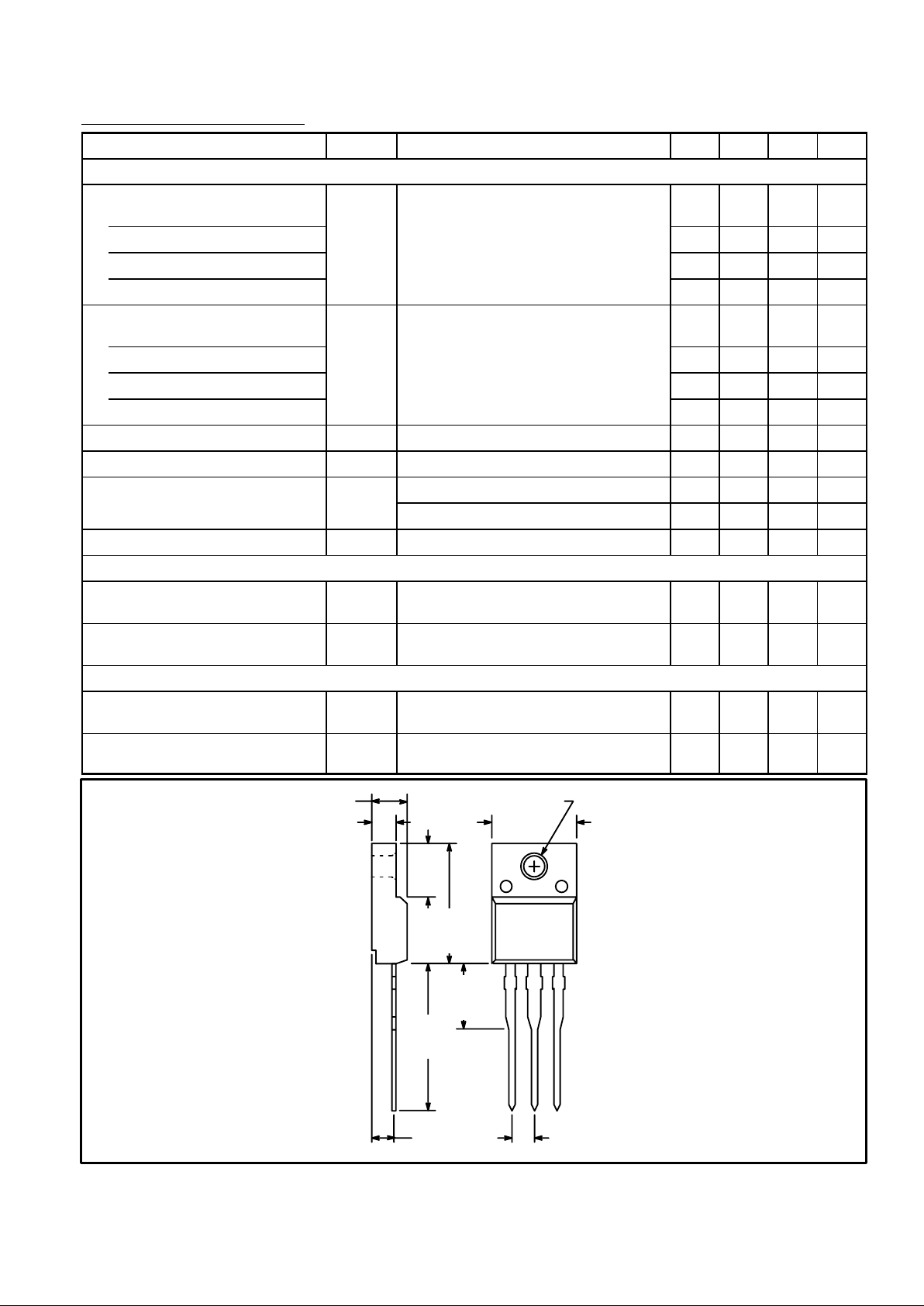
.126 (3.2) Dia Max
.181 (4.6) Max
.405 (10.3)
Max
.114 (2.9)
.622
(15.0)
Max
.252
(6.4)
.118
(3.0)
Max
MT
1
MT
2
G
Isol
.100 (2.54).098 (2.5)
.531
(13.5)
Min
 Loading...