

NTE NTE5603, NTE5601, NTE5600, NTE5605, NTE5607 Datasheet
...
NTE5600 thru NTE5607
TRIAC, 4 Amp
Description:
The NTE5600 through NTE5607 TRIACs are designed primarily for full–wave AC control applications
such as light dimmers, motor controls, heating controls and power supplies; or wherever full–wave
silicon gate controlled solid–state devices are needed. TRIAC type thyristors switch from a blocking
to a conducting s tate f or e ither p olari ty o f a ppl ied a node voltage w ith p ositive o r n egative g ate t ri ggering.
Features:
D 2 Mode Gate Triggering
D Blocking Voltages to 600V
D All Diffused and Glass Passivated Junctions for Greater Parameters Uniformity and Stability
Absolute Maximum Ratings:
Repetitive Peak Off–State Voltage (TC = +110°C, Note 1), V
NTE5600 25V. . . . . . . . . . . . . . . . . . . . . . . . . . . . . . . . . . . . . . . . . . . . . . . . . . . . . . . . . . . . . . . . . . . .
NTE5601 50V. . . . . . . . . . . . . . . . . . . . . . . . . . . . . . . . . . . . . . . . . . . . . . . . . . . . . . . . . . . . . . . . . . . .
NTE5602 100V. . . . . . . . . . . . . . . . . . . . . . . . . . . . . . . . . . . . . . . . . . . . . . . . . . . . . . . . . . . . . . . . . . .
NTE5603 200V. . . . . . . . . . . . . . . . . . . . . . . . . . . . . . . . . . . . . . . . . . . . . . . . . . . . . . . . . . . . . . . . . . .
NTE5604 300V. . . . . . . . . . . . . . . . . . . . . . . . . . . . . . . . . . . . . . . . . . . . . . . . . . . . . . . . . . . . . . . . . . .
NTE5605 400V. . . . . . . . . . . . . . . . . . . . . . . . . . . . . . . . . . . . . . . . . . . . . . . . . . . . . . . . . . . . . . . . . . .
NTE5606 500V. . . . . . . . . . . . . . . . . . . . . . . . . . . . . . . . . . . . . . . . . . . . . . . . . . . . . . . . . . . . . . . . . . .
NTE5607 600V. . . . . . . . . . . . . . . . . . . . . . . . . . . . . . . . . . . . . . . . . . . . . . . . . . . . . . . . . . . . . . . . . . .
RMS On–State Current (TC = +85°C), I
T(RMS)
Peak Surge Current (One Full Cycle, 60Hz, TJ = –40° to +110°C), I
Circuit Fusing (t = 8.3ms), I2t 3.7A2s. . . . . . . . . . . . . . . . . . . . . . . . . . . . . . . . . . . . . . . . . . . . . . . . . . . . .
Peak Gate Power, P
Average Gate Power, P
Peak Gate Voltage, V
Operating Junction Temperature Range, T
Storage Temperature Range, T
Thermal Resistance, Junction–to–Case, R
Thermal Resistance, Junction–to–Ambient, R
GM
G(AV)
GM
J
stg
thJC
thJA
Mounting Torque (6–32 Screw, Note 2) 8 in. lb.. . . . . . . . . . . . . . . . . . . . . . . . . . . . . . . . . . . . . . . . . . . . .
DRM
TSM
4A. . . . . . . . . . . . . . . . . . . . . . . . . . . . . . . . . . . . . . . . . . .
30A. . . . . . . . . . . . . . . . . . .
10W. . . . . . . . . . . . . . . . . . . . . . . . . . . . . . . . . . . . . . . . . . . . . . . . . . . . . . . . . . . .
0.5W. . . . . . . . . . . . . . . . . . . . . . . . . . . . . . . . . . . . . . . . . . . . . . . . . . . . . . . .
5V. . . . . . . . . . . . . . . . . . . . . . . . . . . . . . . . . . . . . . . . . . . . . . . . . . . . . . . . . . . . .
–40° to +110°C. . . . . . . . . . . . . . . . . . . . . . . . . . . . . . . . . .
–40° to +150°C. . . . . . . . . . . . . . . . . . . . . . . . . . . . . . . . . . . . . . . . . .
3.5°C/W. . . . . . . . . . . . . . . . . . . . . . . . . . . . . . . . . . . . .
75°C/W. . . . . . . . . . . . . . . . . . . . . . . . . . . . . . . . . . . .
Note 1. Ratings apply for open gate conditions. Thyristor devices shall not be tested with a constant
current source for blocking capability such that the voltage applied exceeds the rated blocking voltage.
Note 2. Torque rating applies with the use of a compression washer. Mounting torque in excess of
8 in. lb. does not appreciably lower case–to–sink thermal resistance. MT2 and heatsink contact pad are common.
Electrical Characteristics: (TC = +25°C unless otherwise specified)
Parameter Symbol Test Conditions Min Typ Max Unit
I
,
Peak Forward or Reverse
Blocking Current
On–State Voltage (Either Direction) V
Peak Gate Trigger Voltage
MT2 (+), G (+); MT2 (–), G (–)
MT2 (+), G (–); MT2 (–), G (+)
DRM
I
RRM
TM
V
GT
Rated V
TJ = +25°C
Rated V
= +110°C
T
J
ITM = 6A Peak – – 2 V
Main Terminal Voltage = 12V,
RL = 100Ω, TJ = –40°C
DRM
DRM
or V
or V
, Gate Open,
RRM
, Gate Open,
RRM
– – 10 µA
– – 2 mA
– 1.4 2.5 V
Peak Gate Trigger Voltage
MT2 (+), G (+); MT2 (–), G (–)
MT2 (+), G (–); MT2 (–), G (+)
Holding Current (Either Direction) I
Turn–On Time (Either Direction) t
Blocking Voltage Application
dv/dt Rated V
Rate at Commutation
Gate Trigger Current
Quads I & III
V
GT
H
on
I
GT
.450
(11.4)
Max
Main Terminal Voltage = Rated V
DRM
,
0.2 – – V
RL = 10kΩ, TJ = +110°C
Main T erminal Voltage = 12V, Gate Open,
– – 70 mA
TJ = –40°C, Initiating Current = 1A
Main T erminal Voltage = 12V, Gate Open,
– – 30 mA
TJ = +25°C
ITM = 14A, IGT = 100mA – 1.5 – µs
, Gate Open, TJ = +85°C – 5 – V/µs
DRM
Main Terminal Voltage = 12V,
– – 30 mA
RL = 100Ω, TJ = +25°C
Main Terminal Voltage = 12V,
– – 60 mA
RL = 100Ω, TJ = –40°C
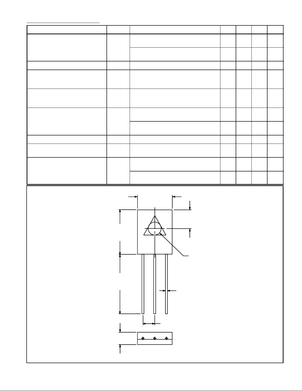
.330 (8.38)
Max
.175
(4.45)
Max
.655
(16.6)
Max
.130 (3.3)
Max
.118 (3.0)
Dia
.030 (.762) Dia
MT1MT2G
.090 (2.28)
 Loading...