

NTE NTE56020 Datasheet

NTE56019 and NTE56020
TRIAC, 25 Amp
Description:
The NTE56019 and NTE56020 are 25 Amp TRIACs with a repetitive peak blocking of 200V and
400V respectively. These devices may be gate triggered from a blocking to conduction state for
either p olari ty of applied v oltage and are d esi gned for A C swi tching and p hase control applicati ons
such as s peed and tem peratur e modulation c ontr ols, lighting c ontr ol s, and st atic switching relays.
The triggering signal is normally applied between the Gate and MT1.
Features:
D Electrically Isolated TO220 Type Package
D Glass–Passivated Junctions
D Surge Capability: Up to 400A
Absolute Maximum Ratings: (TA = +25°C, 60Hz, with a resistive load unless otherwise specified)
Repetitive Peak Blocking Voltage (Note 1), V
NTE56019 200V. . . . . . . . . . . . . . . . . . . . . . . . . . . . . . . . . . . . . . . . . . . . . . . . . . . . . . . . . . . . . . . . .
NTE56020 400V. . . . . . . . . . . . . . . . . . . . . . . . . . . . . . . . . . . . . . . . . . . . . . . . . . . . . . . . . . . . . . . . .
RMS On–State Current (Conduction Angle of 360°, TC = –40° to +125°C), I
Non–Repetitive On–State Current (One Cycle), I
60Hz 250A. . . . . . . . . . . . . . . . . . . . . . . . . . . . . . . . . . . . . . . . . . . . . . . . . . . . . . . . . . . . . . . . . . . . . .
50Hz 208A. . . . . . . . . . . . . . . . . . . . . . . . . . . . . . . . . . . . . . . . . . . . . . . . . . . . . . . . . . . . . . . . . . . . . .
Fusing Current (t = 8.3ms), I2t 259A2s. . . . . . . . . . . . . . . . . . . . . . . . . . . . . . . . . . . . . . . . . . . . . . . . . . . .
Peak Gate Current (Pulse Width ≤ 10µs Max), I
Peak Gate Dissipation (Pulse Width ≤ 10µs, IGT ≤ I
Gate Dissipation, P
G(AV)
Operating Junction Temperature Range, T
Storage Temperature Range, T
stg
Thermal Resistance, Junction–to–Case, R
Thermal Resistance, Junction–to–Ambient, R
Lead Temperature (During Soldering, 1/16” from case, 10sec max), T
Note 1. For either polarity of MT2 with reference to MT1 terminal.
J
thJC
DRM
GM
thJA
TSM
GTM
), P
GM
T(RMS)
25A. . . . . . . . . .
2A. . . . . . . . . . . . . . . . . . . . . . . . . . . . . . . . . . . . . . .
20W. . . . . . . . . . . . . . . . . . . . . . . . . . .
500mW. . . . . . . . . . . . . . . . . . . . . . . . . . . . . . . . . . . . . . . . . . . . . . . . . . . . . . . . . .
–40° to +125°C. . . . . . . . . . . . . . . . . . . . . . . . . . . . . . . . . .
–40° to +125°C. . . . . . . . . . . . . . . . . . . . . . . . . . . . . . . . . . . . . . . . . .
1.5K/W. . . . . . . . . . . . . . . . . . . . . . . . . . . . . . . . . . . . . .
60K/W. . . . . . . . . . . . . . . . . . . . . . . . . . . . . . . . . . . .
L
+230°C. . . . . . . . . . . . . . . . .
Electrical Characteristics: (TA = +25°C unless otherwise specified)
Parameter Symbol Test Conditions Min Typ Max Unit
Off–State Leakage Current I
On–State Voltage V
DRM
TM
VD = V
VD = V
I
T(RMS)
, TJ = +25°C, Note 1 – – 0.1 mA
DRM
, TJ = +125°C, Note 1 – – 3 mA
DRM
= 25A, Note 1 – – 1.8 V
Note 1. For either polarity of MT2 with reference to MT1 terminal.
Electrical Characteristics (Cont’d): (TA = +25°C unless otherwise specified)
Parameter Symbol Test Conditions Min Typ Max Unit
Gate Trigger Current I
GT
Gate Trigger Voltage V
Holding Current I
Gate Controlled Turn–On Time t
Critical Rate–of–Rise dv/dt VD = V
Critical Rate–of–Rise, Off–State dv/dtcVD = V
GT
H
gt
VD = 12V, TC = –40° to +125°C – – 80 mA
VD = 12V, Quadrants I, II, and III, Note 2 – – 2.5 V
Gate Open, Note 1, Note 3 – – 100 mA
IGT = 500mA, 0.1µs Rise Time – 4 – µs
, Gate Open, TC = +1 25°C, Note 1 250 – – V/µs
DRM
, IT = 25A, di/dt = 13.5A/ms,
DRM
Gate Unenergized, Note 1
Note 1. For either polarity of MT2 with reference to MT1 terminal.
Note 2. For either polarity of gate voltage with reference to electrode MT1.
Note 3. Initial On–State Current = 400mA (DC).
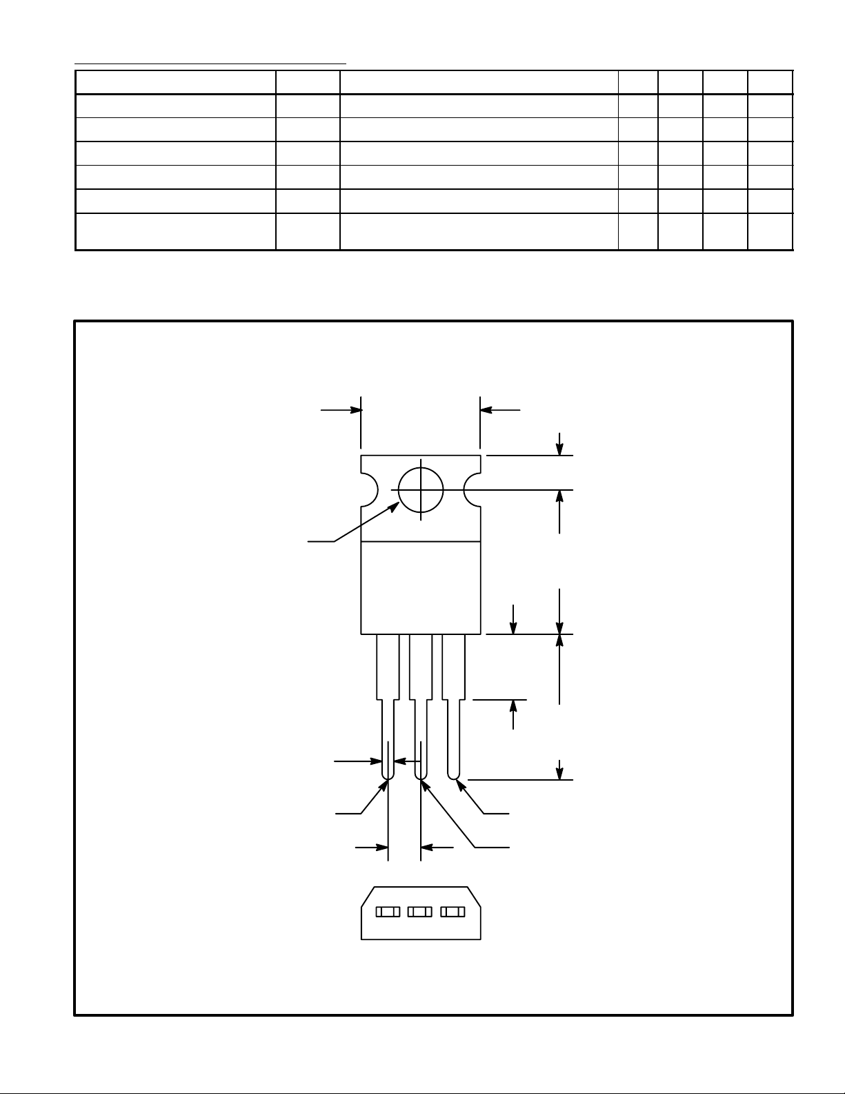
.420 (10.67)
Max
.110 (2.79)
5 – – V/µs
.147 (3.75)
Dia Max
.070 (1.78) Max
MT
.100 (2.54)
Isolated
.500
(12.7)
Max
.250 (6.35)
Max
.500
(12.7)
Min
1
Gate
MT
2
 Loading...