NSC MM78C29J-883 Datasheet

TL/F/5908
MM78C29/MM88C29 Quad Single-Ended Line Driver
MM78C30/MM88C30 Dual Differential Line Driver
February 1996
MM78C29/MM88C29 Quad Single-Ended Line Driver
MM78C30/MM88C30 Dual Differential Line Driver
General Description
The MM78C30/MM88C30 is a dual differential line driver
that also performs the dual four-input NAND or dual four-input AND function. The absence of a clamp diode to V
CC
in
the input protection circuitry of the MM78C30/MM88C30 allows a CMOS user to interface systems operating at different voltage levels. Thus, a CMOS digital signal source can
operate at a V
CC
voltage greater than the VCCvoltage of
the MM78C30 line driver. The differential output of the
MM78C30/MM88C30 eliminates ground-loop errors.
The MM78C29/MM88C29 is a non-inverting single-wire
transmission line driver. Since the output ON resistance is a
low 20X typ., the device can be used to drive lamps, relays,
solenoids, and clock lines, besides driving data lines.
Features
Y
Wide supply voltage range 3V to 15V
Y
High noise immunity 0.45 VCC(typ.)
Y
Low output ON resistance 20X (typ.)
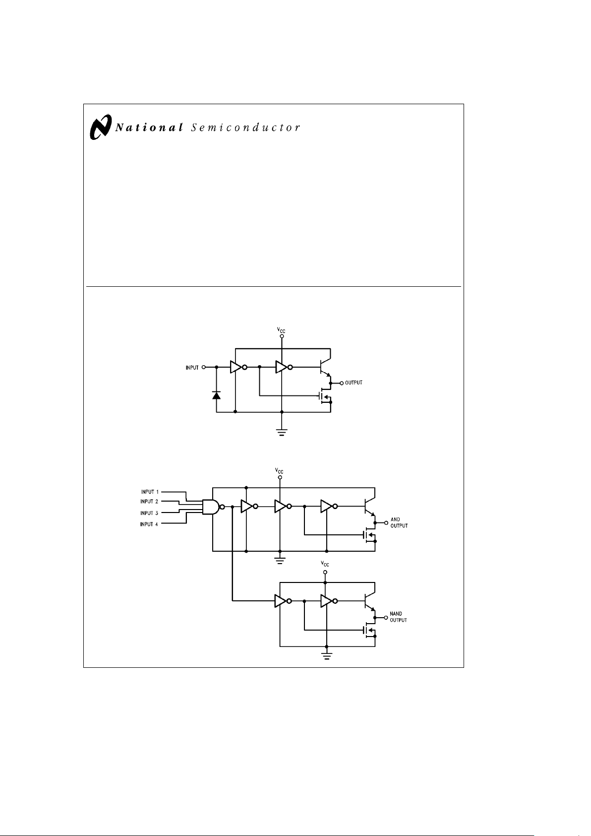
Logic Diagrams
1/4 MM78C29/MM88C29
TL/F/5908– 1
1/2 MM78C30/MM88C30
TL/F/5908– 2
C
1996 National Semiconductor Corporation RRD-B30M36/Printed in U. S. A.
http://www.national.com

Absolute Maximum Ratings (Note 1)
If Military/Aerospace specified devices are required,
please contact the National Semiconductor Sales
Office/Distributors for availability and specifications.
Voltage at Any Pin (Note 1)
b
0.3V to V
CC
a
16V
Operating Temperature Range
MM78C29/MM78C30
b
55§Ctoa125§C
MM88C29/MM88C30
b
40§Ctoa85§C
Storage Temperature
b
65§Ctoa150§C
Power Dissipation (PD)
Dual-In-Line 700 mW
Small Outline 500 mW
Operating V
CC
Range 3V to 15V
Absolute Maximum V
CC
18V
Average Current at Output
MM78C30/MM88C30 50 mA
MM78C29/MM88C29 25 mA
Maximum Junction Temperature, T
j
150§C
Lead Temperature
(Soldering, 10 seconds) 260
§
C
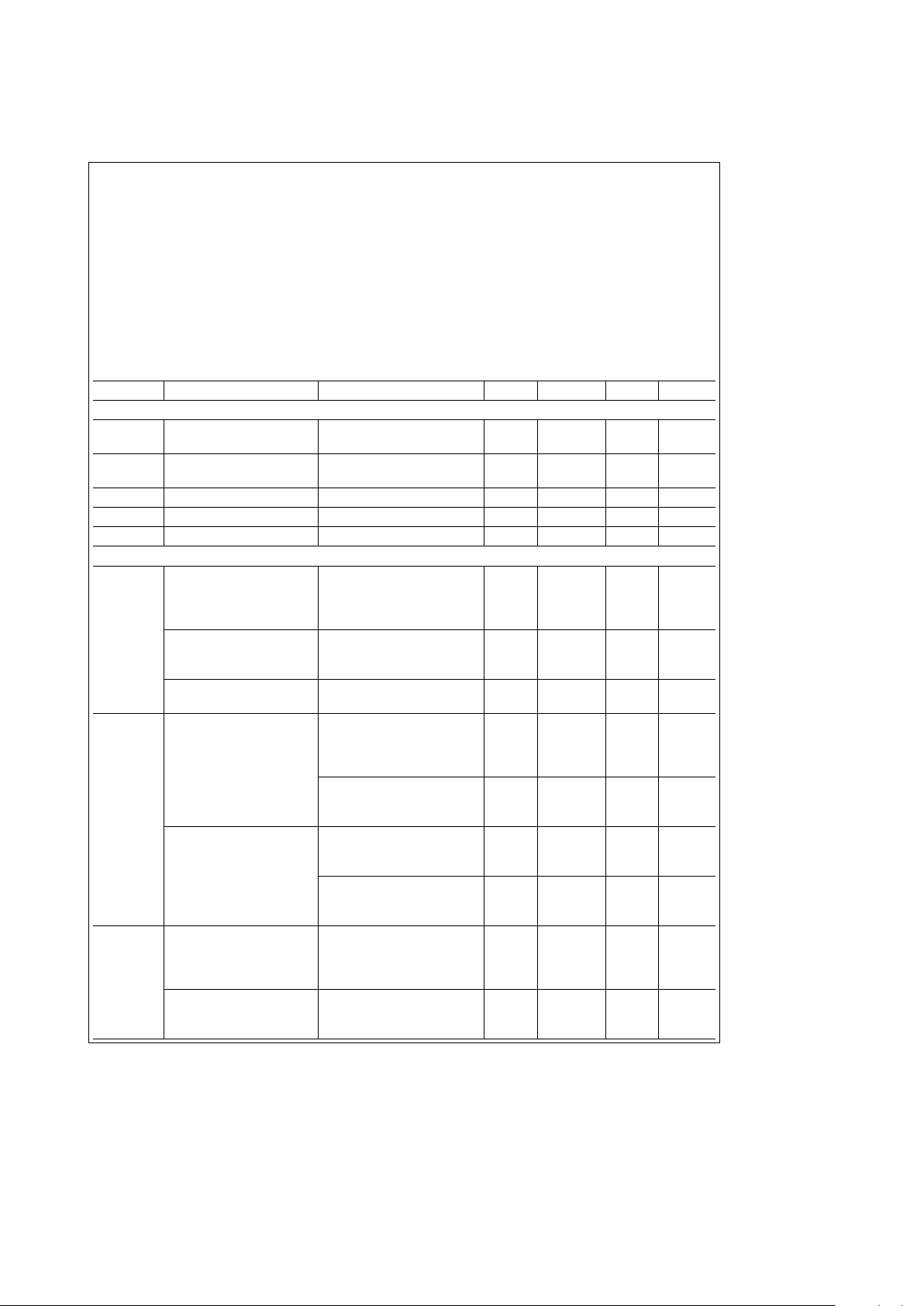
DC Electrical Characteristics Min/Max limits apply across temperature range unless otherwise noted
Symbol Parameter Conditions Min Typ Max Units
CMOS TO CMOS
V
IN(1)
Logical ‘‘1’’ Input Voltage V
CC
e
5V 3.5 V
V
CC
e
10V 8 V
V
IN(0)
Logical ‘‘0’’ Input Voltage V
CC
e
5V 1.5 V
V
CC
e
10V 2 V
I
IN(1)
Logical ‘‘1’’ Input Current V
CC
e
15V, V
IN
e
15V 0.005 1 mA
I
IN(0)
Logical ‘‘0’’ Input Current V
CC
e
15V, V
IN
e
0V
b
1
b
0.005 mA
I
CC
Supply Current V
CC
e
5V 0.05 100 mA
OUTPUT DRIVE
I
SOURCE
Output Source Current
MM78C29/MM78C30 V
OUT
e
V
CC
b
1.6V,
V
CC
t
4.5V, T
j
e
25§C
b
57
b
80 mA
T
j
e
125§C
b
32
b
50 mA
MM88C29/MM88C30 V
OUT
e
V
CC
b
1.6V,
V
CC
t
4.75V, T
j
e
25§C
b
47
b
80 mA
T
j
e
85§C
b
32
b
60 mA
MM78C29/MM88C29 V
OUT
e
V
CC
b
0.8V
b
2
b
20 mA
MM78C30/MM88C30 V
CC
t
4.5V
I
SINK
Output Sink Current
MM78C29/MM78C30 V
OUT
e
0.4V, V
CC
e
4.5V,
T
j
e
25§C1120mA
T
j
e
125§C 8 14 mA
V
OUT
e
0.4V, V
CC
e
10V,
T
j
e
25§C2240mA
T
j
e
125§C1628mA
MM88C29/MM88C30 V
OUT
e
0.4V, V
CC
e
4.75V,
T
j
e
25§C 9.5 22 mA
T
j
e
85§C 8 18 mA
V
OUT
e
0.4V, V
CC
e
10V,
T
j
e
25§C1940mA
T
j
e
125§C 15.5 33 mA
I
SOURCE
Output Source Resistance
MM78C29/MM78C30 V
OUT
e
V
CC
b
1.6V,
V
CC
t
4.5V, T
j
e
25§C2028X
T
j
e
125§C3250X
MM88C29/MM88C30 V
OUT
e
V
CC
b
1.6V,
V
CC
t
4.75V, T
j
e
25§C2034X
T
j
e
85§C2750X
http://www.national.com 2

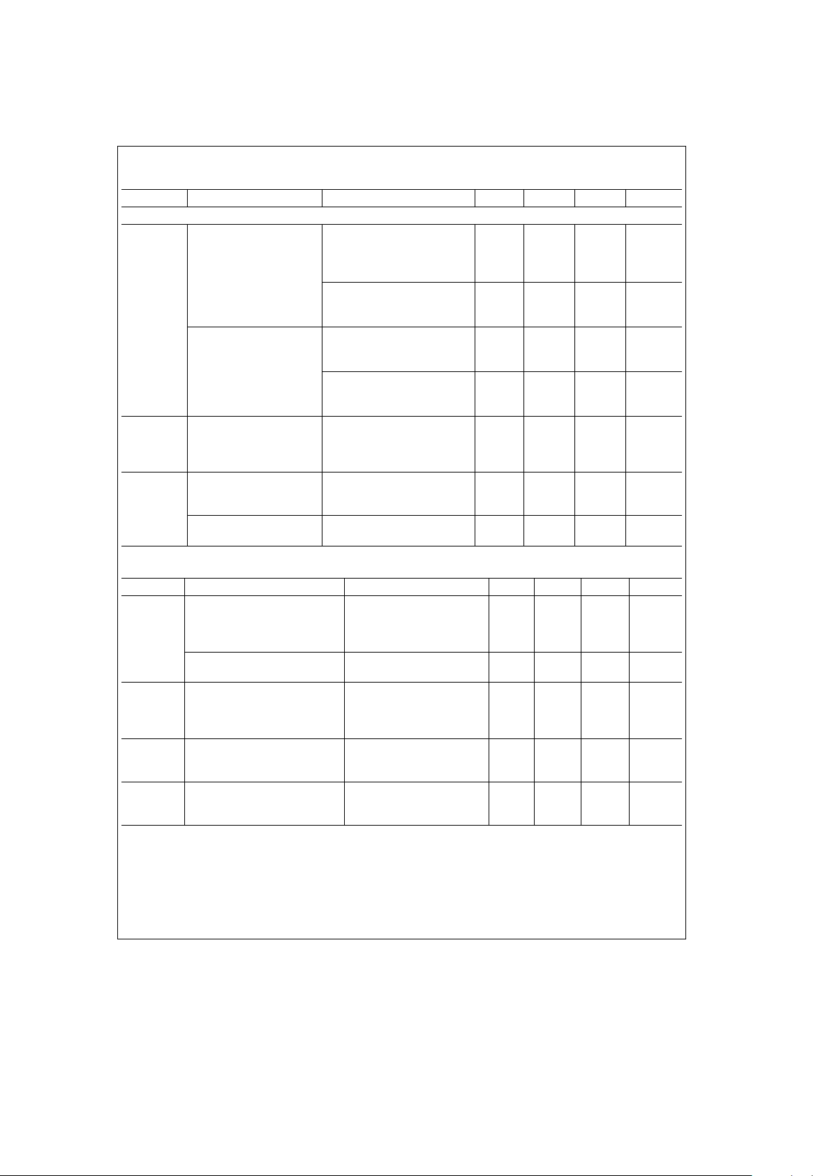
DC Electrical Characteristics
Min/Max limits apply across temperature range, unless otherwise noted (Continued)
Symbol Parameter Conditions Min Typ Max Units
OUTPUT DRIVE (Continued)
I
SINK
Output Sink Resistance
MM78C29/MM78C30 V
OUT
e
0.4V, V
CC
e
4.50V,
T
j
e
25§C2036X
T
j
e
125§C2850X
V
OUT
e
0.4V, V
CC
e
10V,
T
j
e
25§C1018X
T
j
e
125§C1425X
MM88C29/MM88C30 V
OUT
e
0.4V, V
CC
e
4.75V,
T
j
e
25§C1841X
T
j
e
85§C2250X
V
OUT
e
0.4V, V
CC
e
10V,
T
j
e
25§C1021X
T
j
e
85§C1226X
Output Resistance
Temperature Coefficient
Source 0.55 %/
§
C
Sink 0.40 %/
§
C
i
JA
Thermal Resistance
MM78C29/MM78C30 100
§
C/W
(D-Package)
MM88C29/MM88C30
150
§
C/W
(N-Package)
AC Electrical Characteristics* T
A
e
25§C, C
L
e
50 pF
Symbol Parameter Conditions Min Typ Max Units
t
pd
Propagation Delay Time to
Logical ‘‘1’’ or ‘‘0’’ (See
Figure 2
)
MM78C29/MM88C29 V
CC
e
5V 80 200 ns
V
CC
e
10V 35 100 ns
MM78C30/MM88C30 V
CC
e
5V 110 350 ns
V
CC
e
10V 50 150 ns
t
pd
Differential Propagation Delay R
L
e
100X,C
L
e
5000 pF
Time to Logical ‘‘1’’ or ‘‘0’’ (See
Figure 1
)
MM78C30/MM88C30 V
CC
e
5V 400 ns
V
CC
e
10V 150 ns
C
IN
Input Capacitance
MM78C29/MM88C29 (Note 3) 5.0 pF
MM78C30/MM88C30 (Note 3) 5.0 pF
C
PD
Power Dissipation Capacitance
MM78C29/MM88C29 (Note 3) 150 pF
MM78C30/MM88C30 (Note 3) 200 pF
*AC Parameters are guaranteed by DC correlated testing.
Note 1: ‘‘Absolute Maximum Ratings’’ are those values beyond which the safety of the device cannot be guaranteed. Except for ‘‘Operating Temperature Range’’
they are not meant to imply that the devices should be operated at these limits. The table of ‘‘Electrical Characteristics’’ provides conditions for actual device
operation.
Note 2: Capacitance is guaranteed by periodic testing.
Note 3: C
PD
determines the no load AC power consumption of any CMOS device. For complete explanation see 54C/74C Family Characteristics application note
AN-90 (CMOS Logic Databook).
http://www.national.com3
 Loading...