NSC MM58342N Datasheet

MM58342 High Voltage Display Driver
MM58342 High Voltage Display Driver
February 1995
General Description
The MM58342 is a monolithic MOS integrated circuit utilizing CMOS metal gate low threshold P- and N-channel devices. It is available both in 28-pin molded dual-in-line packages or as dice. The MM58342 is particularly suited for driving high voltage (35V max) vacuum fluorescent (VF) displays (e.g., a 20-digit alphanumeric or dot matrix display).
Applications
Y
COPSTMor microprocessor-driven displays
Y
Instrumentation readouts
Y
Industrial control indicator
Y
Digital clock, thermostat, counter, voltmeter
Y
Word processor text displays
Y
Automotive dashboards
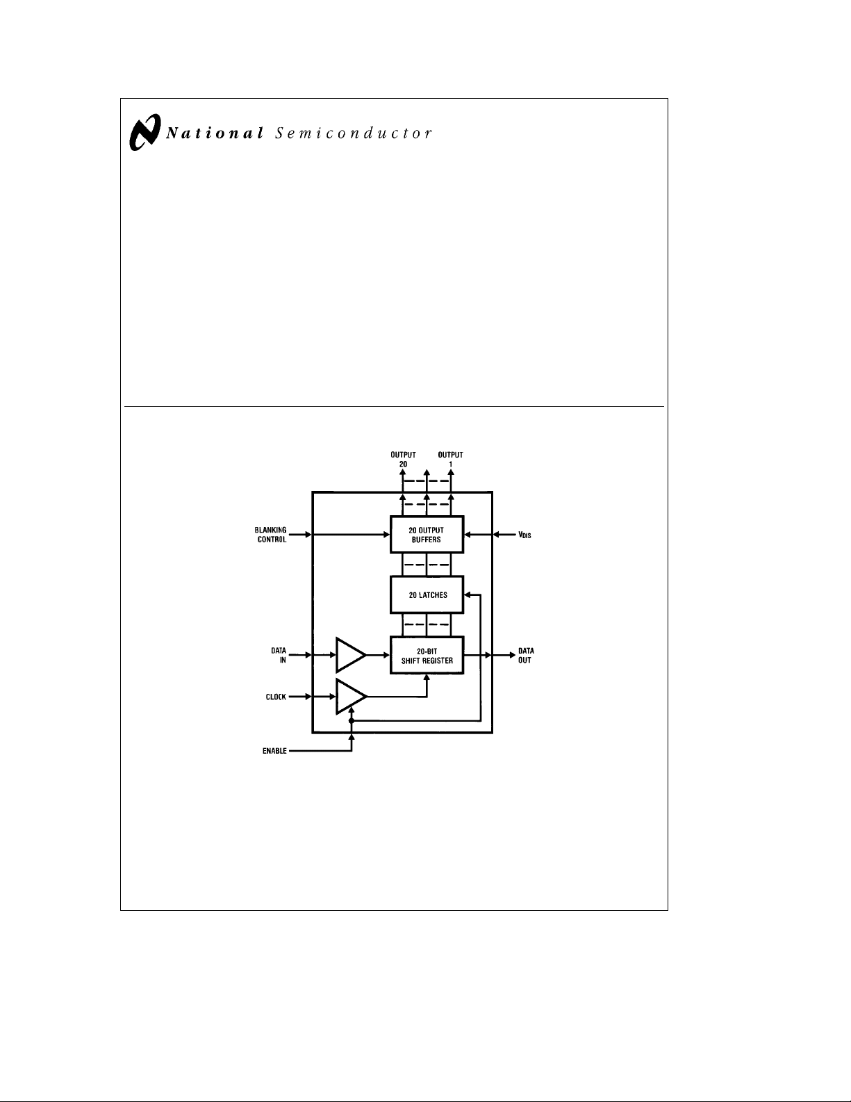
Block Diagram
Features
Y
Direct interface to high voltage display
Y
Serial data input
Y
No external resistors required
Y
Wide display power supply operation
Y
LSTTL compatible inputs
Y
Software compatible with NS display driver family
Y
Compatible with alphanumeric or dot matrix displays
Y
Display blanking control input
Y
Simple to cascade
FIGURE 1
TL/F/7925– 1
COPSTMis a trademark of National Semiconductor Corporation.
C
1995 National Semiconductor Corporation RRD-B30M105/Printed in U. S. A.
TL/F/7925

Absolute Maximum Ratings
If Military/Aerospace specified devices are required,
please contact the National Semiconductor Sales
Office/Distributors for availability and specifications.
Voltage at Any Input Pin V
Voltage at Any Display Pin VDDto V
a
V
V
l
DIS
l
DD
Storage Temperature
DD
a
0.3V to V
SS
DD
b
65§Ctoa150§C
b
b
36.5V
36.5V
0.3V
Operating Conditions
Supply Voltage (V
e
V
0V 4.5 5.5 V
SS
Display Voltage (V
Temperature Range
DD
DIS
Min Max Units
)
b
)
30
b
40
b
10 V
a
85
C
§
Power Dissipation at 25§C
Molded DIP Package, Board Mount 2.03W*
Molded DIP Package, Socket Mount 1.83W**
Junction Temperature 130
C
§
Lead Temperature (Soldering, 10 sec.) 260§C
*Molded DIP Package, Board Mount, i
derate 19.2 mW/
C above 25§C.
§
**Molded DIP Package, Socket Mount, i
derate 17.2 mW/
C above 25§C.
§
JA
JA
e
52§C/W,
e
58§C/W,
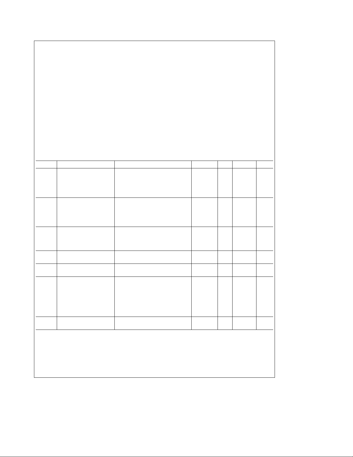
DC Electrical Characteristics
eb
T
40§Ctoa85§C, V
A
Symbol Parameter Conditions Min Typ Max Units
Power Supply Currents
I
DD
I
DIS
Input Logic Levels
DATA IN, CLOCK
ENABLE, BLANK
V
IL
V
IH
Logic ‘0’ 0.8 V
Logic ‘1’ (Note 1) 2.4 V
Data Output Logic Levels
V
OL
V
OH
V
OH
I
IN
C
IN
Logic ‘0’ I
Logic ‘1’ I
Logic ‘1’ I
Input Currents DATA IN, V
CLOCK ENABLE, BLANK
Input Capacitance DATA IN,
CLOCK ENABLE, BLANK
Display Output Impedances V
R
OFF
R
ON
V
DOL
Note 1: 74LSTTL V
Output Off
Output On
Display Output Low Voltage V
e
OH
DD
(Figure 3a)
(Figure 3b)
2.7V@I
OUT
e
5Vg0.5V, V
eb
400 mA, TTL V
e
0V unless otherwise specified
SS
e
V
VSSor VDD,V
IN
V
Disconnected
DIS
e
V
5.5V, V
DD
All Outputs Low
e
400 mA 0.4 V
OUT
eb
OUT
OUT
V
V
V
V
V
V
b
10 mAV
eb
500 mA 2.8 V
e
0V or V
IN
DD
DIS
DIS
DIS
DIS
DIS
DIS
DD
30VsV
OH
DD
e
5.5V, V
eb
10V 55 250 kX
eb
20V 60 300 kX
eb
30V 65 400 kX
eb
10V 700 800 X
eb
20V 600 750 X
eb
30V 500 680 X
e
5.5V, I
OUT
DIS
e
2.4V@I
SS
SS
s
b
OUT
e
SS
e
0V, V
e
0V
e
Open Circuit,
10V
eb
400 mA.
DIS
0V,
eb
30V
b
0.5 V
DD
b
10 10 mA
V
DIS
150 mA
10 mA
15 pF
a
V
2V
DIS
2
 Loading...