TL/F/11219
MM58274C Microprocessor Compatible Real Time Clock
April 1991
MM58274C
Microprocessor Compatible Real Time Clock
General Description
The MM58274C is fabricated using low threshold metal gate
CMOS technology and is designed to operate in bus oriented microprocessor systems where a real time clock and calendar function are required. The on-chip 32.768 kHz crystal
controlled oscillator will maintain timekeeping down to 2.2V
to allow low power standby battery operation. This device is
pin compatible with the MM58174A but continues timekeeping up to tens of years. The MM58274C is a direct replacement for the MM58274 offering improved Bus access cycle
times.
Applications
Y
Point of sale terminals
Y
Teller terminals
Y
Word processors
Y
Data logging
Y
Industrial process control
Features
Y
Same pin-out as MM58174A, MM58274B, and
MM58274
Y
Timekeeping from tenths of seconds to tens of years in
independently accessible registers
Y
Leap year register
Y
Hours counter programmable for 12 or 24-hour
operation
Y
Buffered crystal frequency output in test mode for easy
oscillator setting
Y
Data-changed flag allows simple testing for time
rollover
Y
Independent interrupting time with open drain output
Y
Fully TTL compatible
Y
Low power standby operation (10 mA at 2.2V)
Y
Low cost 16-pin DIP and 20-pin PCC
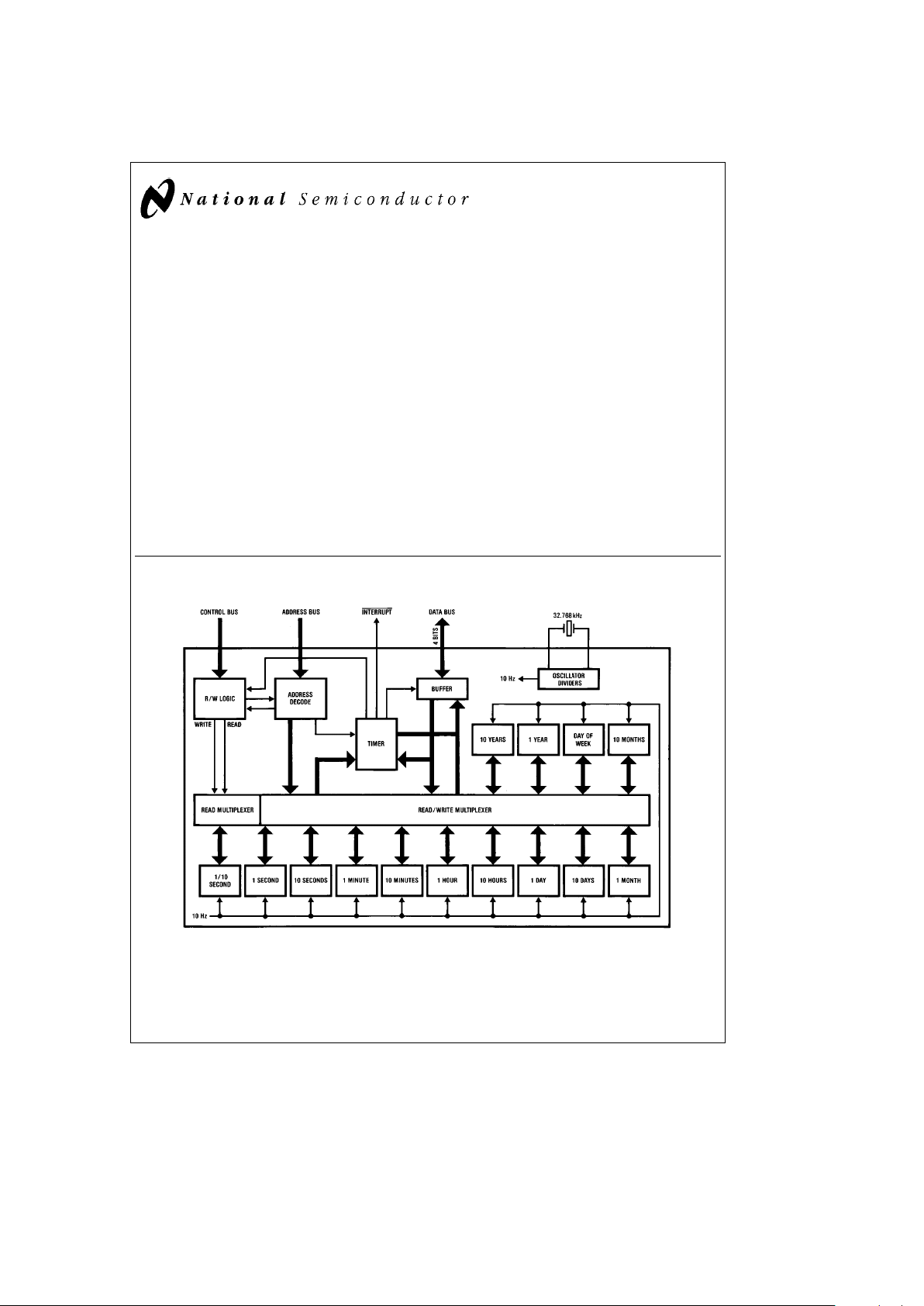
Block Diagram
TL/F/11219– 1
FIGURE 1
TRI-STATEÉis a registered trademark of National Semiconductor Corp.
Microbus
TM
is a trademark of National Semiconductor Corp.
C
1995 National Semiconductor Corporation RRD-B30M105/Printed in U. S. A.
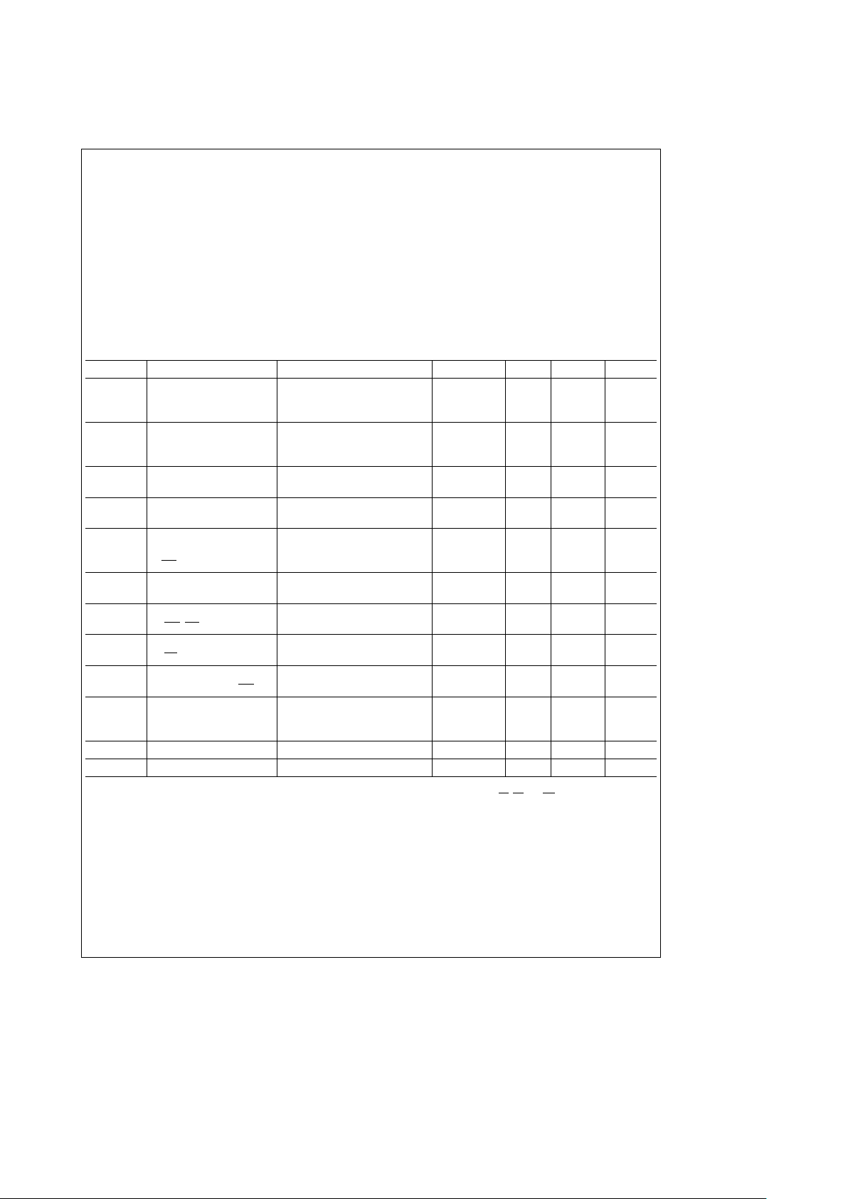
Absolute Maximum Ratings (Note 1)
If Military/Aerospace specified devices are required,
please contact the National Semiconductor Sales
Office/Distributors for availability and specifications.
DC Input or Output Voltage
b
0.3V to V
DD
a
0.3V
DC Input or Output Diode Current
g
5.0 mA
Storage Temperature, T
STG
b
65§Ctoa150§C
Supply Voltage, V
DD
6.5V
Power Dissipation, P
D
500 mW
Lead Temperature
(Soldering, 10 seconds) 260
§
Operating Conditions
Min Max Units
Operating Supply Voltage 4.5 5.5 V
Standby Mode Supply Voltage 2.2 5.5 V
DC Input or Output Voltage 0 V
DD
V
Operating Temperature Range
b
40 85
§
C
Electrical Characteristics V
DD
e
5Vg10%, Teb40§Ctoa85§C unless otherwise stated.
Symbol Parameter Conditions Min Typ Max Units
V
IH
High Level Input 2.0 V
Voltage (except
XTAL IN)
V
IL
Low Level Input 0.8 V
Voltage (except
XTAL IN)
V
OH
High Level Output I
OH
eb
20 mAV
DD
b
0.1 V
Voltage (DB0–DB3) I
OH
eb
1.6 mA 3.7 V
V
OH
High Level Output I
OH
eb
20 mAV
DD
b
0.1 V
Voltage (INT) (In Test Mode)
V
OL
Low Level Output I
OL
e
20 mA 0.1 V
Voltage (DB0–DB3, i
OL
e
1.6 mA 0.4 V
INT)
I
IL
Low Level Input Current V
IN
e
VSS(Note 2)
b
5
b
80 mA
(AD0–AD3, DB0 –DB3)
I
IL
Low Level Input Current V
IN
e
VSS(Note 2)
b
5
b
190 mA
(WR
,RD)
I
IL
Low Level Input Current V
IN
e
VSS(Note 2)
b
5
b
550 mA
(CS)
I
OZH
Ouput High Level V
OUT
e
V
DD
2.0 mA
Leakage Current (INT
)
I
DD
Average Supply Current All V
IN
e
VCCor Open Circuit
V
DD
e
2.2V (Standby Mode) 4 10 mA
V
DD
e
5.0V (Active Mode) 1 mA
C
IN
Input Capacitance 5 10 pF
C
OUT
Output Capacitance (Outputs Disabled) 10 pF
Note 1: Absolute Maximum Ratings are those values beyond which damage to the device may occur. All voltages referenced to ground unless otherwise noted.
Note 2: The DB0 –DB3 and AD0 –AD3 lines all have active P-channel pull-up transistors which will source current. The CS
,RD, and WR lines have internal pull-up
resistors to V
DD
.
2
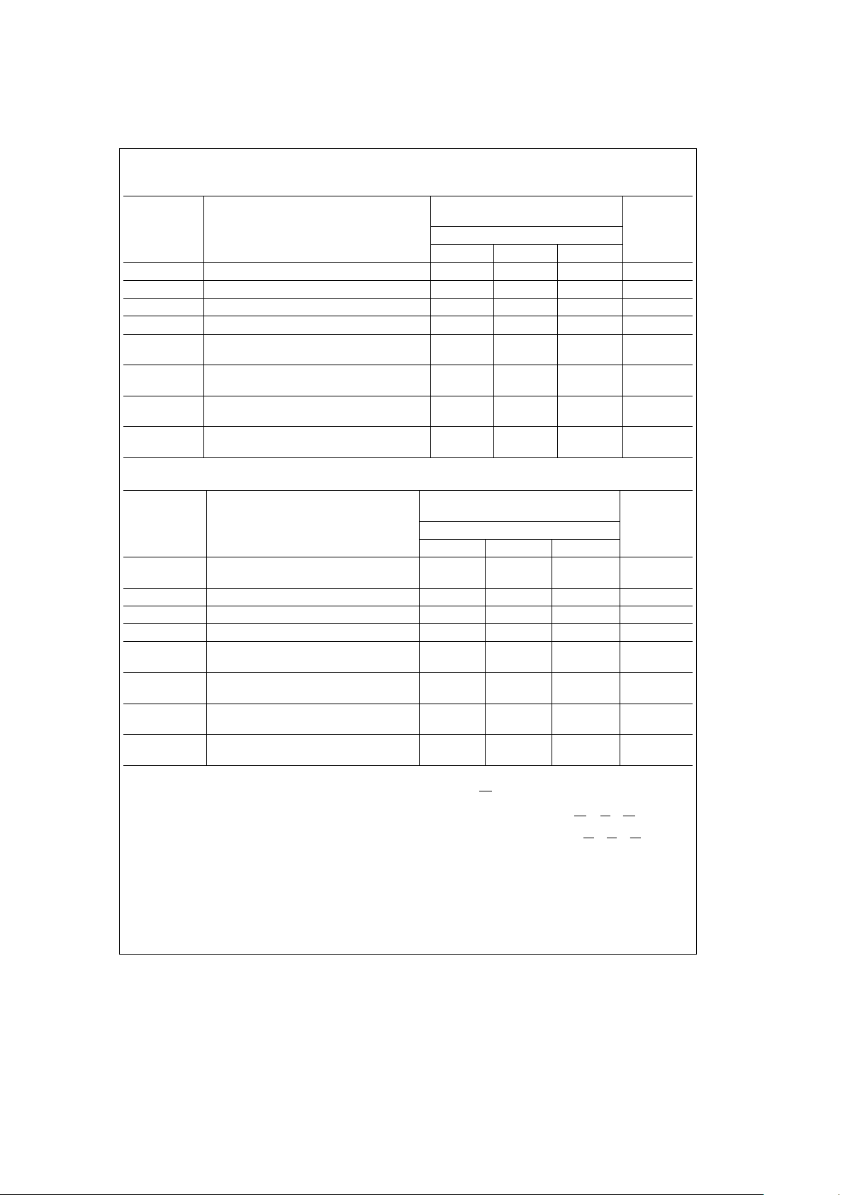
AC Switching Characteristics
READ TIMING: DATA FROM PERIPHERAL TO MICROPROCESSOR V
DD
e
5Vg0.5V, C
L
e
100 pF
Commercial
Symbol Parameter
Specification
Units
T
A
eb
40§Ctoa85§C
Min Typ Max
t
AD
Address Bus Valid to Data Valid 390 650 ns
t
CSD
Chip Select On to Data Valid 140 300 ns
t
RD
Read Strobe On to Data Valid 140 300 ns
t
RW
Read Strobe Width (Note 3, Note 7) DC
t
RA
Address Bus Hold Time from Trailing Edge 0 ns
of Read Strobe
t
CSH
Chip Select Hold Time from Trailing Edge 0 ns
of Read Strobe
t
RH
Data Hold Time from Trailing Edge 70 160 ns
of Read Strobe
t
HZ
Time from Trailing Edge of Read Strobe 250 ns
Until O/P Drivers are TRI-STATE
É
WRITE TIMING: DATA FROM MICROPROCESSOR TO PERIPHERAL V
DD
e
5Vg0.5V
Commercial
Symbol Parameter
Specification
Units
T
A
eb
40§Ctoa85§C
Min Typ Max
t
AW
Address Bus Valid to Write Strobe O 400 125 ns
(Note 4, Note 6)
t
CSW
Chip Select On to Write Strobe O 250 100 ns
t
DW
Data Bus Valid to Write Strobe O 400 220 ns
t
WW
Write Strobe Width (Note 6) 250 95 ns
t
WCS
Chip Select Hold Time Following 0 ns
Write Strobe O
t
WA
Address Bus Hold Time Following 0 ns
Write Strobe O
t
WD
Data Bus Hold Time Following 100 35 ns
Write Strobe O
t
AWS
Address Bus Valid Before 70 20 ns
Start of Write Strobe
Note 3: Except for special case restriction: with interrupts programmed, max read strobe width of control register (ADDR 0) is 30 ms. See section on Interrupt
Programming.
Note 4: All timings measured to the trailing edge of write strobe (data latched by the trailing edge of WR
).
Note 5: Input test waveform peak voltages are 2.4V and 0.4V. Output signals are measured to their 2.4V and 0.4V levels.
Note 6: Write strobe as used in the Write Timing Table is defined as the period when both chip select and write inputs are low, ie., WS
,eCSaWR. Hence write
strobe commences when both signals are low, and terminates when the first signal returns high.
Note 7: Read strobe as used in the Read Timing Table is defined as the period when both chip select and read inputs are low, ie., RS
eCSa
RD.
Note 8: Typical numbers are at V
CC
e
5.0V and T
A
e
25§C.
3
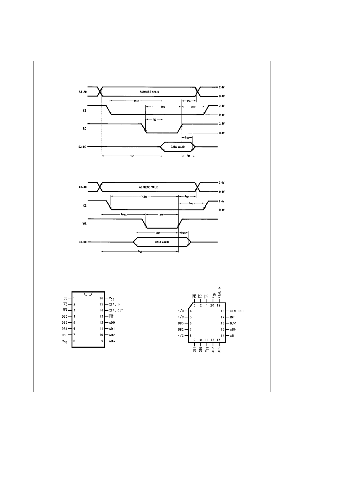
Switching Time Waveforms
Read Cycle Timing (Notes 5 and 7)
TL/F/11219– 2
Write Cycle Timing (Notes 5 and 6)
TL/F/11219– 3
Connection Diagrams
Dual-In-Line Package
TL/F/11219– 4
Top View
PCC Package
TL/F/11219– 5
Top View
FIGURE 2
Order Number MM58274CJ, MM58274CN or MM58274CV
See NS Package J16A, N16A, or V20A
4
Functional Description
The MM58274C is a bus oriented microprocessor real time
clock. It has the same pin-out as the MM58174A while offering extended timekeeping up to units and tens of years. To
enhance the device further, a number of other features have
been added including: 12 or 24 hours counting, a testable
data-changed flag giving easy error-free time reading and
simplified interrupt control.
A buffered oscillator signal appears on the interrupt output
when the device is in test mode. This allows for easy oscillator setting when the device is initially powered up in a system.
The counters are arranged as 4-bit words and can be randomly accessed for time reading and setting. The counters
output in BCD (binary coded decimal) 4-bit numbers. Any
register which has less than 4 bits (e.g., days of week uses
only 3 bits) will return a logic 0 on any unused bits. When
written to, the unused inputs will be ignored.
Writing a logic 1 to the clock start/stop control bit resets the
internal oscillator divider chain and the tenths of seconds
counter. Writing a logic 0 will start the clock timing from the
nearest second. The time then updates every 100 ms with
all counters changing synchronously. Time changing during
a read is detected by testing the data-changed bit of the
control register after completing a string of clock register
reads.
Interrupt delay times of 0.1s, 0.5s, 1s, 5s, 10s, 30s or 60s
can be selected with single or repeated interrupt outputs.
The open drain output is pulled low whenever the interrupt
timer times out and is cleared by reading the control register.
CIRCUIT DESCRIPTION
The block diagram in
Figure 1
shows the internal structure
of the chip. The 16-pin package outline is shown in
Figure 2
.
Crystal Oscillator
This consists of a CMOS inverter/amplifier with an on-chip
bias resistor. Externally a 20 pF capacitor,a6pF–36pF
trimmer capacitor and a crystal are suggested to complete
the 32.768 kHz timekeeping oscillator circuit.
The 6 pF –36 pF trimmer fine tunes the crystal load impedance, optimizing the oscillator stability. When properly adjusted (i.e., to the crystal frequency of 32.768 kHz), the circuit will display a frequency variation with voltage of less
than 3 ppm/V. When an external oscillator is used, connect
to oscillator input and float (no connection) the oscillator
output.
When the chip is enabled into test mode, the oscillator is
gated onto the interrupt output pin giving a buffered oscillator output that can be used to set the crystal frequency
when the device is installed in a system. For further information see the section on Test Mode.
Divider Chain
The crystal oscillator is divided down in three stages to produce a 10 Hz frequency setting pulse. The first stage is a
non-integer divider which reduces the 32.768 kHz input to
30.720 kHz. This is further divided by a 9-stage binary ripple
counter giving an output frequency of 60 Hz. A 3-stage
Johnson counter divides this by six, generating a 10 Hz output. The 10 Hz clock is gated with the 32.768 kHz crystal
frequency to provide clock setting pulses of 15.26 ms duration. The setting pulse drives all the time registers on the
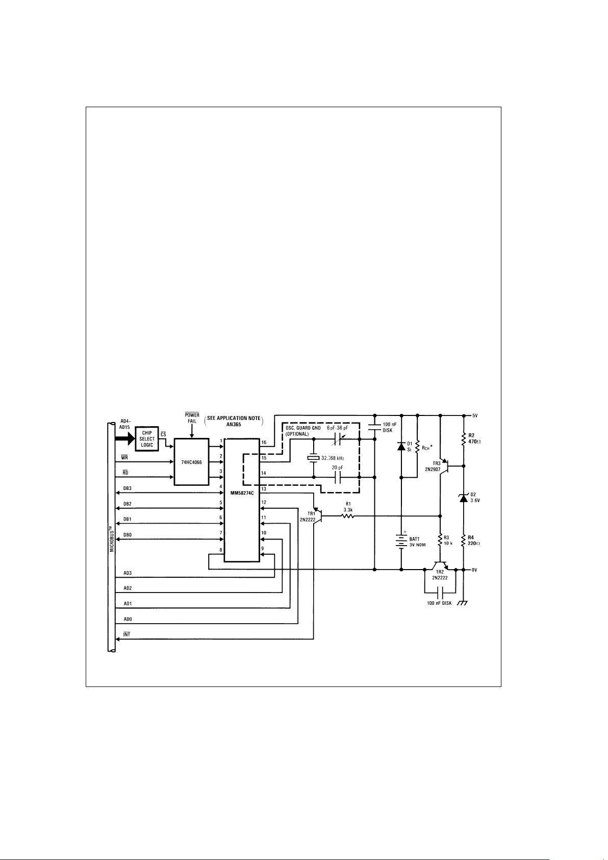
*Use resistor with Ni-cad cells only
TL/F/11219– 6
FIGURE 3. Typical System Connection Diagram
5
 Loading...