NSC MM54C914J-883 Datasheet

TL/F/5917
MM54C914/MM74C914 Hex Schmitt Trigger with Extended Input Voltage
February 1988
MM54C914/MM74C914 Hex Schmitt
Trigger with Extended Input Voltage
General Description
The MM54C914/MM74C914 is a monolithic CMOS Hex
Schmitt trigger with special input protection scheme. This
scheme allows the input voltage levels to exceed V
CC
or
ground by at least 10V (V
CC
b
25V to GNDa25V), and is
valuable for applications involving voltage level shifting or
mismatched power supplies.
The positive and negative-going threshold voltages, V
T
a
and V
T
b
, show low variation with respect to temperature
(typ 0.0005V/
§
CatV
CC
e
10V). And the hysteresis,
V
T
a
b
V
T
b
t
0.2 VCCis guaranteed.
Features
Y
Hysteresis 0.45 VCC(typ.)
0.2 V
CC
guaranteed
Y
Special input protection Extended Input
Voltage Range
Y
Wide supply voltage range 3V to 15V
Y
High noise immunity 0.7 VCC(typ.)
Y
Low power TTL Fan out of 2
compatibility driving 74L
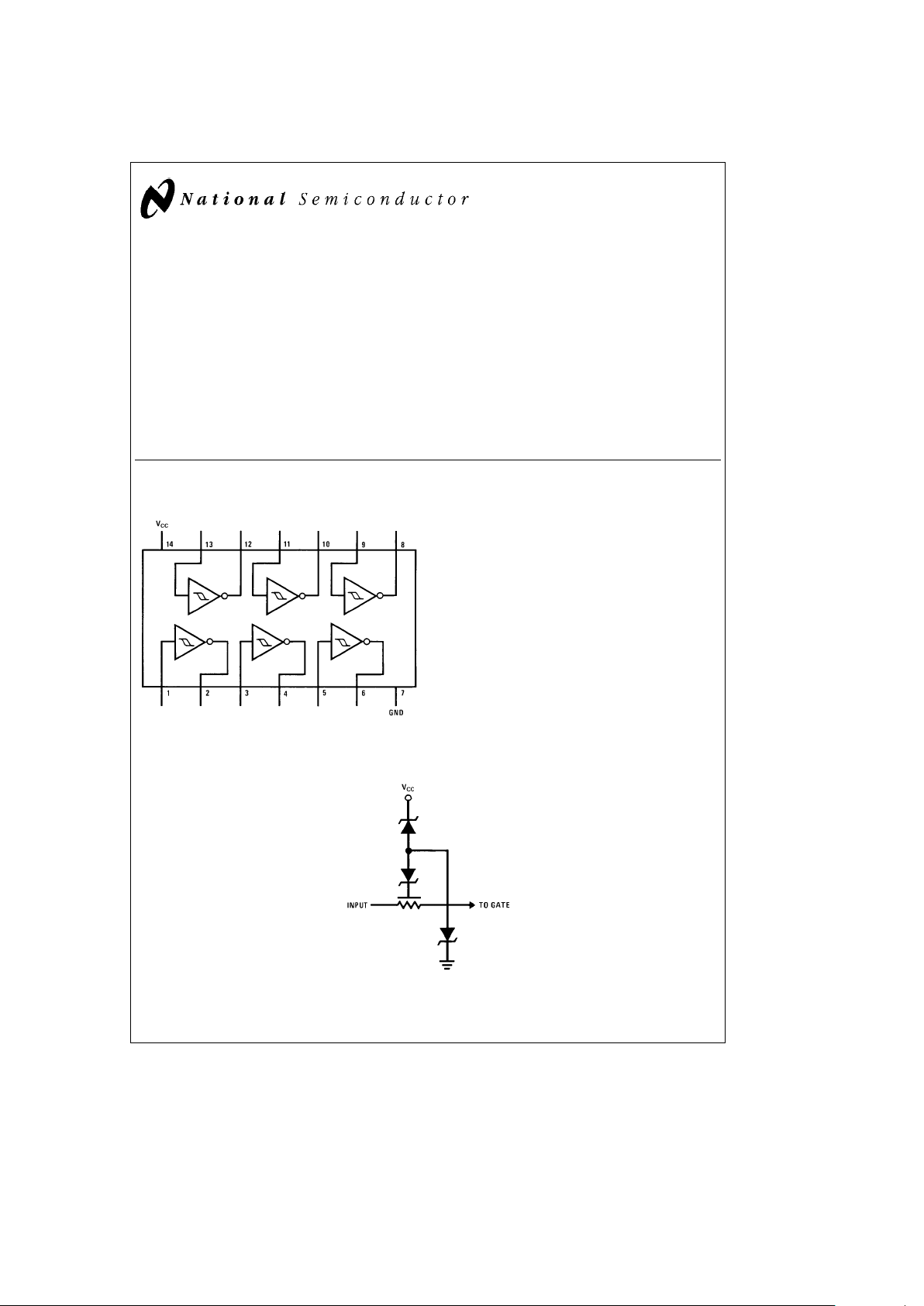
Connection Diagram
Dual-In-Line Package
TL/F/5917– 1
Top View
Order Number MM54C914 or MM74C914
Special Input Protection
8V&25V
for the diodes.
TL/F/5917– 2
C
1995 National Semiconductor Corporation RRD-B30M105/Printed in U. S. A.

Absolute Maximum Ratings (Note 1)
If Military/Aerospace specified devices are required,
please contact the National Semiconductor Sales
Office/Distributors for availability and specifications.
Voltage at any Input Pin V
CC
b
25V to GNDa25V
Voltage at any other Pin
b
0.3V to V
CC
a
0.3V
Operating Temperature Range (T
A
)
MM54C914
b
55§Ctoa125§C
MM74C914
b
40§Ctoa85§C
Storage Temperature Range (T
S
)
b
65§Ctoa150§C
Power Dissipation
Dual-In-Line 700 mW
Small Outline 500 mW
Operating V
CC
Range 3V to 15V
Absolute Maximum (V
CC
) 18V
Lead Temperature (TL)
(Soldering, 10 seconds) 300
§
C
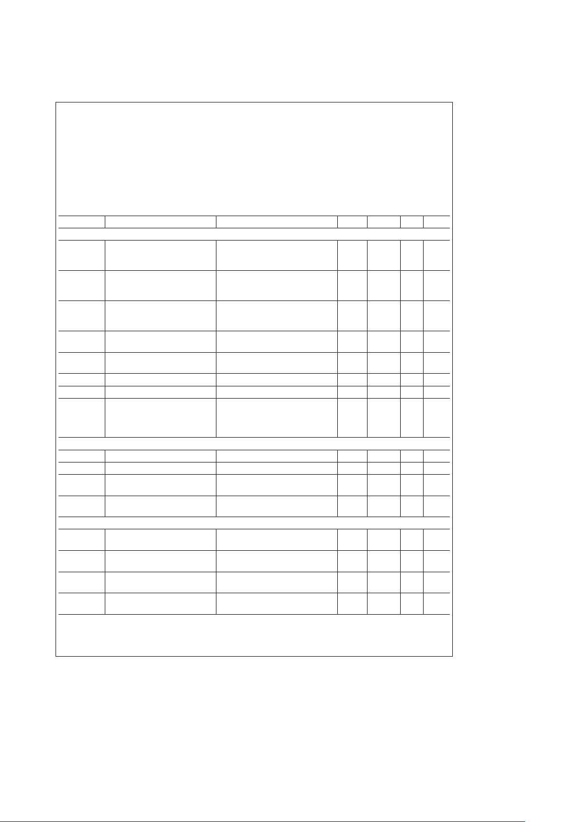
DC Electrical Characteristics Min/Max limits apply across temperature range unless otherwise noted
Symbol Parameter Conditions Min Typ Max Units
CMOS TO CMOS
V
T
a
Positive Going Threshold Voltage V
CC
e
5V 3.0 3.6 4.3
V
V
CC
e
10V 6.0 6.8 8.6
V
V
CC
e
15V 9.0 10 12.9
V
T
b
Negative Going Threshold Voltage V
CC
e
5V 0.7 1.4 2.0
V
V
CC
e
10V 1.4 3.2 4.0
V
V
CC
e
15V 2.1 5 6.0
V
T
a
b
V
T
b
Hysteresis V
CC
e
5V 1.0 2.2 3.6 V
V
CC
e
10V 2.0 3.6 7.2 V
V
CC
e
15V 3.0 5 10.8 V
V
OUT(1)
Logical ‘‘1’’ Output Voltage V
CC
e
5V, I
O
eb
10 mA 4.5 V
V
CC
e
10V, I
O
eb
10 mA 9.0 V
V
OUT(0)
Logical ‘‘0’’ Output Voltage V
CC
e
5V, I
O
ea
10 mA 0.5 V
V
CC
e
10V, I
O
ea
10 mA 1.0 V
I
IN(1)
Logical ‘‘1’’ Input Current V
CC
e
15V, V
IN
e
25V 0.005 5.0 mA
I
IN(0)
Logical ‘‘0’’ Input Current V
CC
e
15V, V
IN
eb
10V
b
100b0.005 mA
I
CC
Supply Current V
CC
e
15V, V
IN
eb
10V/25V 0.05 300 mA
V
CC
e
5V, V
IN
eb
2.5V (Note 4) 20 mA
V
CC
e
10V, V
IN
e
5V (Note 4) 200 mA
V
CC
e
15V, V
IN
e
7.5V (Note 4) 600 mA
CMOS/LPTTL INTERFACE
V
IN(1)
Logical ‘‘1’’ Input Voltage V
CC
e
5V 4.3 V
V
IN(0)
Logical ‘‘0’’ Input Voltage V
CC
e
5V 0.7 V
V
OUT(1)
Logical ‘‘1’’ Output Voltage 54C, V
CC
e
4.5V, I
O
eb
360 mA 2.4 V
74C, V
CC
e
4.75V, I
O
eb
360 mA 2.4 V
V
OUT(0)
Logical ‘‘0’’ Output Voltage 54C, V
CC
e
4.5V, I
O
e
360 mA 0.4 V
74C, V
CC
e
4.75V, I
O
e
360 mA 0.4 V
OUTPUT DRIVE (See 54C/74C Family Characteristics Data Sheet) (Short Circuit Current)
I
SOURCE
Output Source Current V
CC
e
5V, V
OUT
e
0V, T
A
e
25§C
b
1.75
b
3.3 mA
(P-Channel)
I
SOURCE
Output Source Current V
CC
e
10V, V
OUT
e
0V, T
A
e
25§C
b
8.0
b
15 mA
(P-Channel)
I
SINK
Output Sink Current V
CC
e
5V, V
OUT
e
VCC,T
A
e
25§C
1.75 3.6 mA
(N-Channel)
I
SINK
Output Sink Current V
CC
e
10V, V
OUT
e
VCC,T
A
e
25§C
8.0 16 mA
(N-Channel)
2
 Loading...