

NSC MM54C86J-883 Datasheet
TL/F/5887
MM54C86/MM74C86 Quad 2-Input EXCLUSIVE-OR Gate
February 1988
MM54C86/MM74C86 Quad 2-Input EXCLUSIVE-OR Gate
General Description
Employing complementary MOS (CMOS) transistors to
achieve wide power supply operating range, low power consumption and high noise margin these gates provide basic
functions used in the implementation of digital integrated
circuit systems. The N- and P-channel enhancement mode
transistors provide a symmetrical circuit with output swing
essentially equal to the supply voltage. No DC power other
than that caused by leakage current is consumed during
static condition. All inputs are protected from damage due
to static discharge by diode clamps to V
CC
and GND.
Features
Y
Wide supply voltage range 3.0V to 15V
Y
Guaranteed noise margin 1.0V
Y
High noise immunity 0.45 VCC(typ.)
Y
Low power Fan out of 2
TTL compatibility driving 74L
Y
Low power consumption 10 nW/package (typ.)
Y
The MM54C86/MM74C86 follows the
MM54LS86/MM74LS86 Pinout
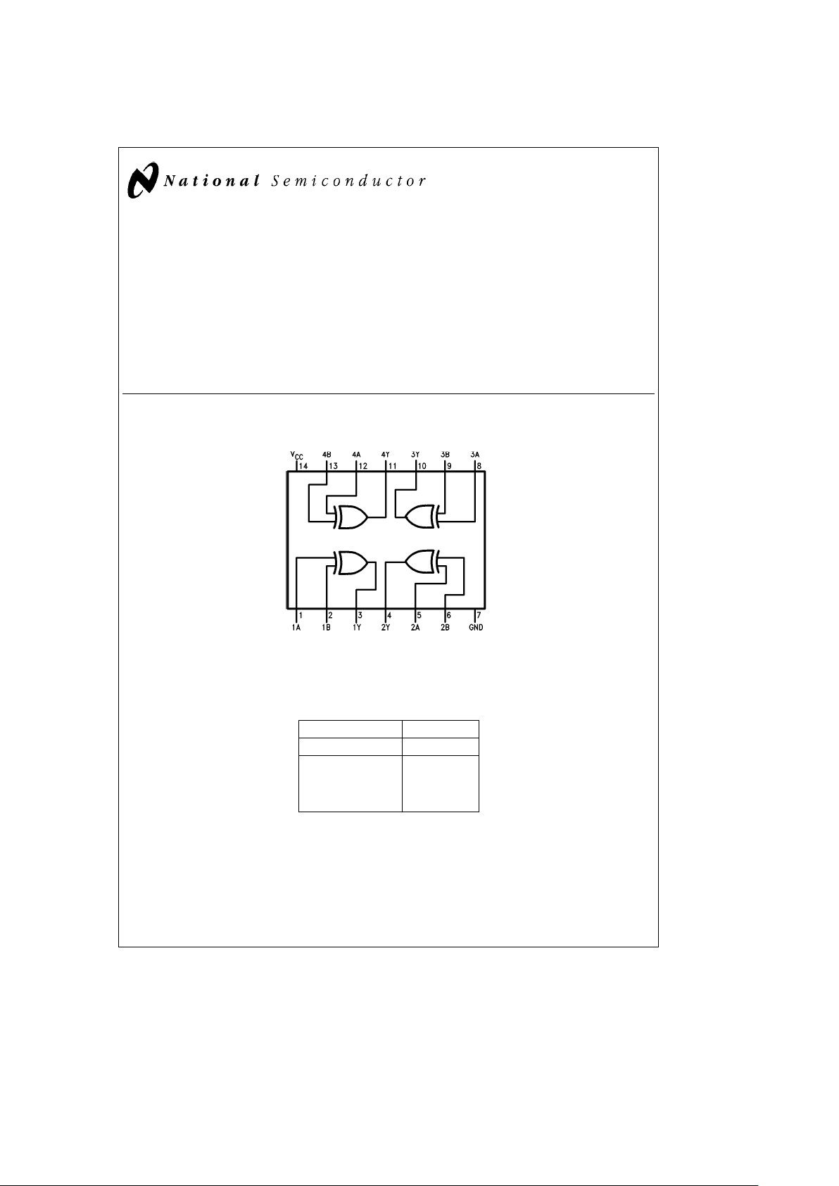
Connection Diagram
Dual-In-Line Package
TL/F/5887– 1
Top View
Order Number MM54C86 or MM74C86
Truth Table
Inputs Output
AB Y
LL L
LH H
HL H
HH L
H
e
High Level LeLow Level
C
1995 National Semiconductor Corporation RRD-B30M105/Printed in U. S. A.
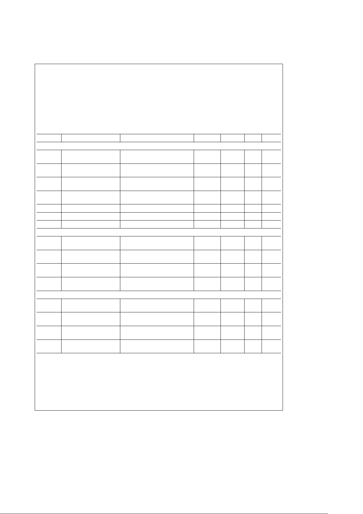
Absolute Maximum Ratings
If Military/Aerospace specified devices are required,
please contact the National Semiconductor Sales
Office/Distributors for availability and specifications.
Voltage at any Pin (Note 1)
b
0.3V to V
CC
a
0.3V
Operating Temperature Range
MM54C86
b
55§Ctoa125§C
MM74C86
b
40§Ctoa85§C
Storage Temperature Range
b
65§Ctoa150§C
Power Dissipation (P
D
)
Dual-In-Line Package 700 mW
Small Outline 500 mW
Operating Range (V
CC
) 3.0V to 15V
Absolute Maximum (VCC) 18V
Lead Temperature (Soldering, 10 seconds) 260
§
C
DC Electrical Characteristics Min/max limits apply across temperature range unless otherwise noted
Symbol Parameter Conditions Min Typ Max Units
CMOS TO CMOS
V
IN(1)
Logical ‘‘1’’ Input Voltage V
CC
e
5.0V 3.5 V
V
CC
e
10V 8.0 V
V
IN(0)
Logical ‘‘0’’ Input Voltage V
CC
e
5.0V 1.5 V
V
CC
e
10V 2.0 V
V
OUT(1)
Logical ‘‘1’’ Output Voltage V
CC
e
5.0V, I
O
eb
10 mA 4.5 V
V
CC
e
10V, I
O
eb
10 mA 9.0 V
V
OUT(0)
Logical ‘‘0’’ Output Voltage V
CC
e
5.0V, I
O
ea
10 mA 0.5 V
V
CC
e
10V, I
O
ea
10 mA 1.0 V
I
IN(1)
Logical ‘‘1’’ Input Current V
CC
e
15V, V
IN
e
15V 0.005 1.0 mA
I
IN(0)
Logical ‘‘0’’ Input Current V
CC
e
15V, V
IN
e
0V
b
1.0
b
0.005 mA
I
CC
Supply Current V
CC
e
15V 0.01 15 mA
CMOS/LPTTL INTERFACE
V
IN(1)
Logical ‘‘1’’ Input Voltage 54C, V
CC
e
4.5V V
CC
b
1.5 V
74C, V
CC
e
4.75V V
CC
b
1.5 V
V
IN(0)
Logical ‘‘0’’ Input Voltage 54C, V
CC
e
4.5V 0.8 V
74C, V
CC
e
4.75V 0.8 V
V
OUT(1)
Logical ‘‘1’’ Output Voltage 54C, V
CC
e
4.5V, I
O
eb
360 mA 2.4 V
74C, V
CC
e
4.75V, I
O
eb
360 mA 2.4 V
V
OUT(0)
Logical ‘‘0’’ Output Voltage 54C, V
CC
e
4.5V, I
O
e
360 mA 0.4 V
74C, V
CC
e
4.75V, I
O
e
360 mA 0.4 V
OUTPUT DRIVE (See 54/74C Family Characteristics Data Sheet) (Short Circuit Current)
I
SOURCE
Output Source Current V
CC
e
5.0V, V
OUT
e
0V
b
1.75
b
3.3 mA
(P-Channel) T
A
e
25§C
I
SOURCE
Output Source Current V
CC
e
10V, V
OUT
e
0V
b
8.0
b
15 mA
(P-Channel) T
A
e
25§C
I
SINK
Output Sink Current V
CC
e
5.0V, V
OUT
e
V
CC
1.75 3.6 mA
(N-Channel) T
A
e
25§C
I
SINK
Output Sink Current V
CC
e
10V, V
OUT
e
V
CC
8.0 16 mA
(N-Channel) T
A
e
25§C
Note 1: ‘‘Absolute Maximum Ratings’’ are those values beyond which the safety of the device cannot be guaranteed. Except for ‘‘Operating Temperature Range’’
they are not meant to imply that the devices should be operated at these limits. The table of ‘‘Electrical Characteristics’’ provides conditions for actual device
operation.
2
 Loading...