NSC MM54C244J-MIL Datasheet

TL/F/5905
MM54C240/MM74C240 Inverting, MM54C244/MM74C244 Non-Inverting
Octal Buffers and Line Drivers with TRI-STATE Outputs
February 1988
MM54C240/MM74C240 Inverting
MM54C244/MM74C244 Non-Inverting
Octal Buffers and Line Drivers with TRI-STATE
É
Outputs
General Description
These octal buffers and line drivers are monolithic complementary MOS (CMOS) integrated circuits with TRI-STATE
outputs. These outputs have been specially designed to
drive highly capacitive loads such as bus-oriented systems.
These devices have a fan out of 6 low power Schottky
loads. A high logic level on the output disable control input
G makes the outputs go into the high impedance state. For
improved TTL input compatibility see MM74C941.
Features
Y
Wide supply voltage range (3V to 15V)
Y
High noise immunity (0.45 VCCtyp)
Y
Low power consumption
Y
High capacitive load drive capability
Y
TRI-STATE outputs
Y
Input protection
Y
TTL compatibility
Y
20-pin dual-in-line package
Y
High speed 25 ns (typ.)@10V, 50 pF (MM74C244)
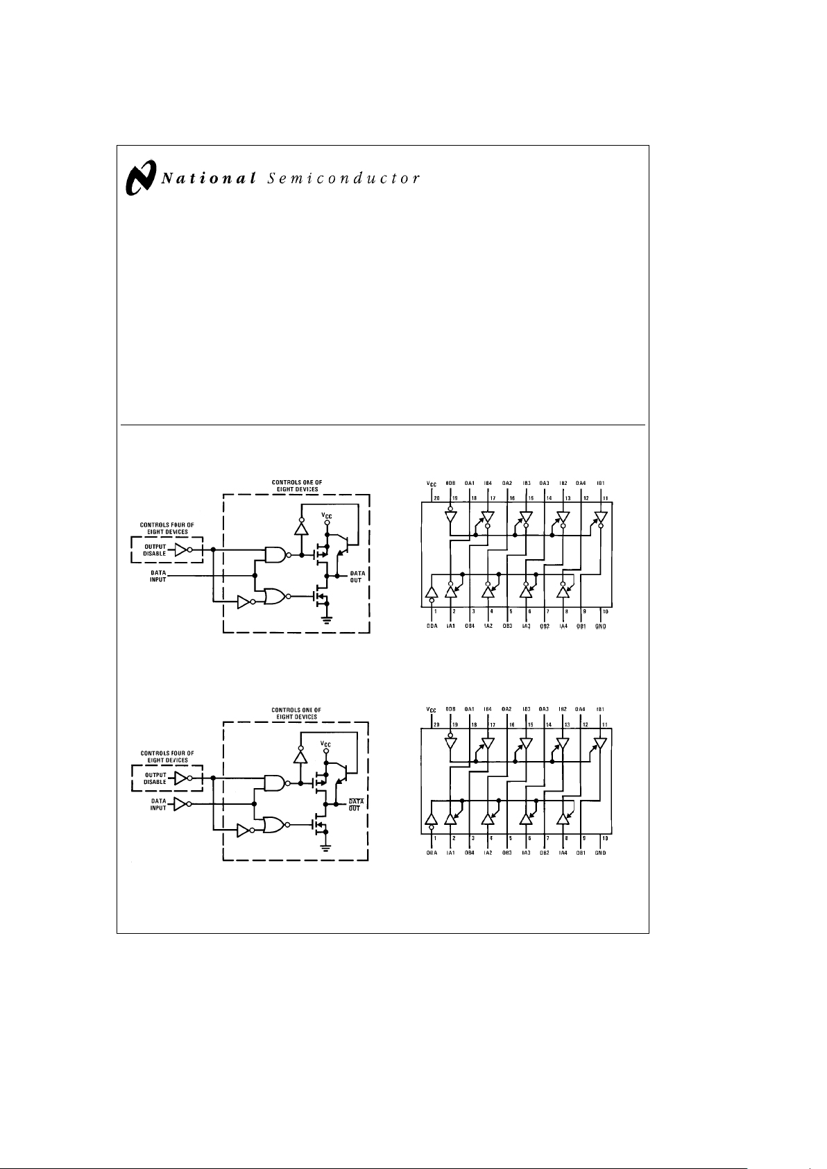
Logic and Connection Diagrams
MM54C240/MM74C240
TL/F/5905– 1
MM54C240/MM74C240 Dual-In-Line Package
TL/F/5905– 2
Top View
Order Number MM54C240 or MM74C240
MM54C244/MM74C244
TL/F/5905– 3
MM54C244/MM74C244 Dual-In-Line Package
TL/F/5905– 4
Top View
Order Number MM54C244 or MM74C244
TRI-STATEÉis a registered trademark of National Semiconductor Corporation.
C
1995 National Semiconductor Corporation RRD-B30M105/Printed in U. S. A.

Absolute Maximum Ratings (Note 1)
If Military/Aerospace specified devices are required,
please contact the National Semiconductor Sales
Office/Distributors for availability and specifications.
Voltage at Any Pin
b
0.3V to V
CC
a
0.3V
Operating Temperature Range
MM54C240, MM54C244
b
55§Ctoa125§C
MM74C240, MM74C244
b
40§Ctoa85§C
Storage Temperature Range
b
65§Ctoa150§C
Power Dissipation
Dual-In-Line 700 mW
Small Outline 500 mW
Operating V
CC
Range 3V to 15V
Absolute Maximum V
CC
18V
Lead Temperature (Soldering, 10 seconds) 260§C
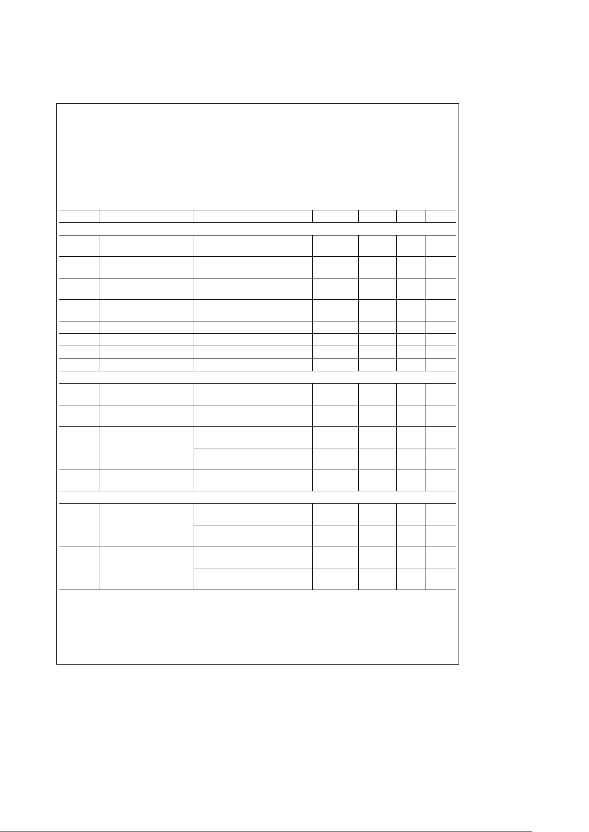
DC Electrical Characteristics Min/Max limits apply across temperature range, unless otherwise noted
Symbol Parameter Conditions Min Typ Max Units
CMOS TO CMOS
V
IN(1)
Logical ‘‘1’’ Input Voltage V
CC
e
5V 3.5 V
V
CC
e
10V 8.0 V
V
IN(0)
Logical ‘‘0’’ Input Voltage V
CC
e
5V 1.5 V
V
CC
e
10V 2.0 V
V
OUT(1)
Logical ‘‘1’’ Output Voltage V
CC
e
5V, I
O
eb
10 mA 4.5 V
V
CC
e
10V, I
O
eb
10 mA 9.0 V
V
OUT(0)
Logical ‘‘0’’ Output Voltage V
CC
e
5V, I
O
e
10 mA 0.5 V
V
CC
e
10V, I
O
e
10 mA 1.0 V
I
OZ
TRI-STATE Output Current V
CC
e
10V, ODeV
IH
g
10 mA
I
IN(1)
Logical ‘‘1’’ Input Current V
CC
e
15V, V
IN
e
15V 0.005 1.0 mA
I
IN(0)
Logical ‘‘0’’ Input Current V
CC
e
15V, V
IN
e
0V
b
1.0
b
0.005 mA
I
CC
Supply Current V
CC
e
15V 0.05 300 mA
CMOS/LPTTL INTERFACE
V
IN(1)
Logical ‘‘1’’ Input Voltage 54C, V
CC
e
4.5V V
CC
b
1.5 V
74C, V
CC
e
4.75V V
CC
b
1.5 V
V
IN(0)
Logical ‘‘0’’ Input Voltage 54C, V
CC
e
4.5V 0.8 V
74C, V
CC
e
4.75V 0.8 V
V
OUT(1)
Logical ‘‘1’’ Output Voltage 54C, V
CC
e
4.5V, I
O
eb
450 mAV
CC
b
0.4 V
74C, V
CC
e
4.75V, I
O
eb
450 mAV
CC
b
0.4 V
54C, V
CC
e
4.5V, I
O
eb
2.2 mA 2.4 V
74C, V
CC
e
4.75V, I
O
eb
2.2 mA 2.4 V
V
OUT(0)
Logical ‘‘0’’ Output Voltage 54C, V
CC
e
4.5V, I
O
e
2.2 mA 0.4 V
74C, V
CC
e
4.75V, I
O
e
2.2 mA 0.4 V
OUTPUT DRIVE (See 54C/74C Family Characteristics Data Sheet) (Short Circuit Current)
I
SOURCE
Output Source Current V
CC
e
5V, V
OUT
e
0V
b
14
b
30 mA
(P-Channel) T
A
e
25§C
V
CC
e
10V, V
OUT
e
0V
b
36
b
70 mA
T
A
e
25§C
I
SINK
Output Sink Current V
CC
e
5V, V
OUT
e
V
CC
12 20 mA
(N-Channel) T
A
e
25§C
V
CC
e
10V, V
OUT
e
V
CC
48 70 mA
T
A
e
25§C
Note 1: ‘‘Absolute Maximum Ratings’’ are those values beyond which the safety of the device cannot be guaranteed. Except for ‘‘Operating Range’’ they are not
meant to imply that the devices should be operated at these limits. The table of ‘‘Electrical Characteristics’’ provides conditions for actual device operation.
2
 Loading...