NSC MM54C195J-883 Datasheet

TL/F/5902
MM54C195/MM74C195 4-Bit Registers
February 1988
MM54C195/MM74C195 4-Bit Registers
General Description
The MM54C195/MM74C195 CMOS 4-bit registers feature
parallel inputs, parallel outputs, J-K serial inputs, shift/load
control input and a direct overriding clear. The following two
modes of operation are possible:
Parallel Load
Shift in direction Q
A
towards Q
D
Parallel loading is accomplished by applying the four bits of
data and taking the shift/load control of input low. The data
is loaded into the associated flip-flops and appears at the
outputs after the positive transition of the clock input. During
parallel loading, serial data flow is inhibited.
Serial shifting is accomplished synchronously when the
shift/load control input is high. Serial data for this mode is
entered at the J-K inputs. These inputs allow the first stage
to perform as a J-K, D, or T-type flip flop as shown in the
truth table.
Features
Y
Medium speed operation 8.5 MHz (typ.) with 10V
supply and 50 pF load
Y
High noise immunity 0.45 VCC(typ.)
Y
Low power 100 nW (typ.)
Y
Tenth power TTL compatible Drive 2 LPTTL loads
Y
Supply voltage range 3V to 15V
Y
Synchronous parallel load
Y
Parallel inputs and outputs from each flip-flop
Y
Direct overriding clear
Y
J and K inputs to first stage
Y
Complementary outputs from last stage
Y
Positive-edge triggered clocking
Y
Diode clamped inputs to protect against static charge
Applications
Y
Automotive
Y
Data terminals
Y
Instrumentation
Y
Medical electronics
Y
Alarm systems
Y
Remote metering
Y
Industrial electronics
Y
Computers
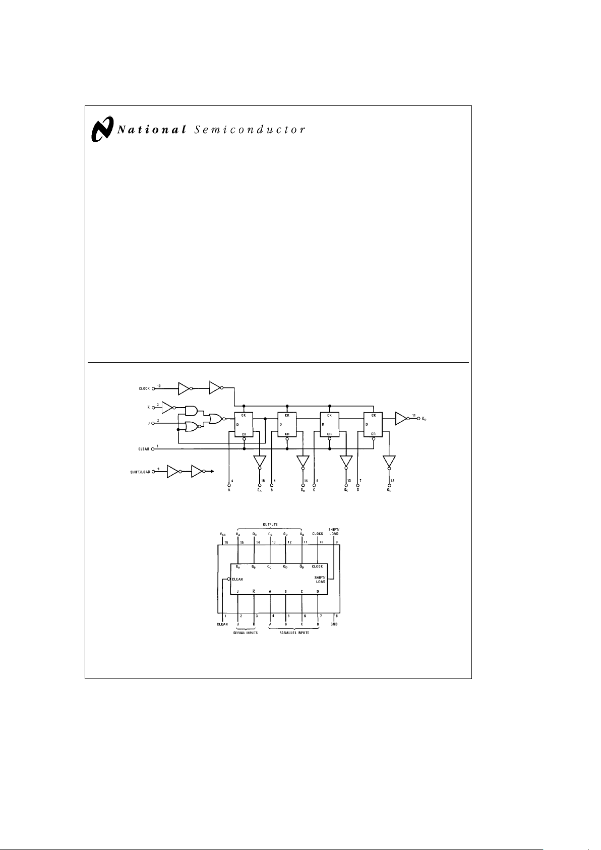
Schematic and Connection Diagrams
Pin 8 to GND
Pin 16 to V
CC
TL/F/5902– 1
Dual-In-Line Package
TL/F/5902– 2
Top View
Order Number MM54C195 or MM74C195
C
1995 National Semiconductor Corporation RRD-B30M105/Printed in U. S. A.

Absolute Maximum Ratings (Note 1)
If Military/Aerospace specified devices are required,
please contact the National Semiconductor Sales
Office/Distributors for availability and specifications.
Voltage at any Pin
b
0.3V to V
CC
a
0.3V
Operating Temperature Range
MM54C195
b
55§Ctoa125§C
MM74C195
b
40§Ctoa85§C
Storage Temperature Range
b
65§Ctoa150§C
Power Dissipation (PD)
Dual-In-Line 700 mW
Small Outline 500 mW
Operating V
CC
Range 3V to 15V
Absolute Maximum V
CC
18V
Lead Temperature (Soldering, 10 sec.) 260§C
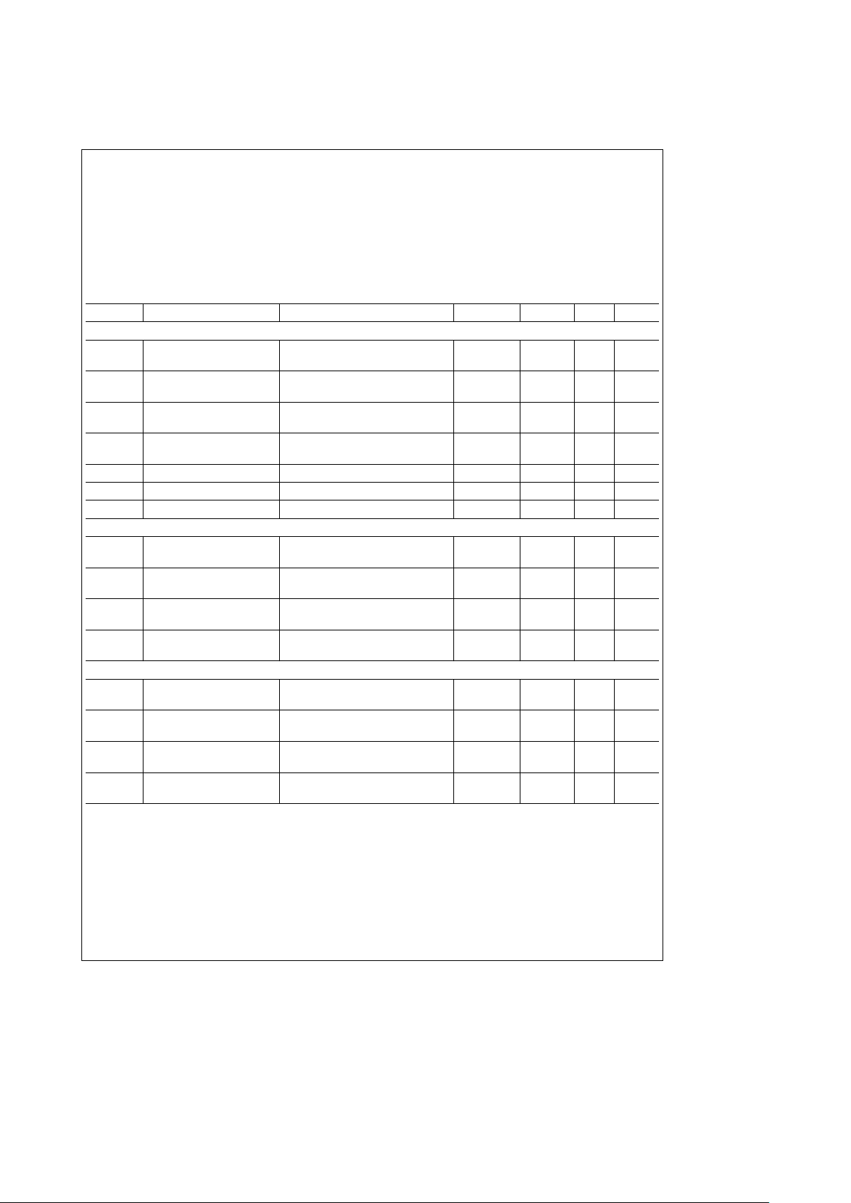
DC Electrical Characteristics Min/Max limits apply across temperature range unless otherwise noted
Symbol Parameter Conditions Min Typ Max Units
CMOS TO CMOS
V
IN(1)
Logical ‘‘1’’ Input Voltage V
CC
e
5V 3.5 V
V
CC
e
10V 8.0 V
V
IN(0)
Logical ‘‘0’’ Input Voltage V
CC
e
5V 1.5 V
V
CC
e
10V 2.0 V
V
OUT(1)
Logical ‘‘1’’ Output Voltage V
CC
e
5V 4.5 V
V
CC
e
10V 9.0 V
V
OUT(0)
Logical ‘‘0’’ Output Voltage V
CC
e
5V 0.5 V
V
CC
e
10V 1.0 V
I
IN(1)
Logical ‘‘1’’ Input Current V
CC
e
15V 0.005 1.0 mA
I
IN(0)
Logical ‘‘0’’ Input Current V
CC
e
15V
b
1.0
b
0.005 mA
I
CC
Supply Current V
CC
e
15V 0.05 300 mA
CMOS/LPTTL INTERFACE
V
IN(1)
Logical ‘‘1’’ Input Voltage 54C V
CC
e
4.5V V
CC
b
1.5 V
74C V
CC
e
4.75V V
CC
b
1.5 V
V
IN(0)
Logical ‘‘0’’ Input Voltage 54C V
CC
e
4.5V 0.8 V
74C V
CC
e
4.75V 0.8 V
V
OUT(1)
Logical ‘‘1’’ Output Voltage 54C V
CC
e
4.5V, I
O
eb
360mA 2.4 V
74C V
CC
e
4.75V, I
O
eb
360mA 2.4 V
V
OUT(0)
Logical ‘‘0’’ Output Voltage 54C V
CC
e
4.5V, I
O
e
360mA 0.4 V
74C V
CC
e
4.75V, I
O
e
360mA 0.4 V
OUTPUT DRIVE (See 54C/74C Family Characteristics Data Sheet) (Short Circuit Current)
I
SOURCE
Output Source Current V
CC
e
5V, V
IN(0)
e
0V
b
1.75 mA
T
A
e
25§C, V
OUT
e
0V
I
SOURCE
Output Source Current V
CC
e
10V, V
IN(0)
e
0V
b
8.0 mA
T
A
e
25§C, V
OUT
e
0V
I
SINK
Output Sink Current V
CC
e
5V, V
IN(1)
e
5V
1.75 mA
T
A
e
25§C, V
OUT
e
V
CC
I
SINK
Output Sink Current V
CC
e
10V, V
IN(1)
e
10V
8.0 mA
T
A
e
25§C, V
OUT
e
V
CC
Note 1: ‘‘Absolute Maximum Ratings’’ are those values beyond which the safety of the device cannot be guaranteed. Except for ‘‘Operating Temperature Range’’
they are not meant to imply that the devices should be operated at these limits. The table of ‘‘Electrical Characteristics’’ provides conditions for actual device
operation.
2
 Loading...