NSC MM54C175J-883 Datasheet

TL/F/5900
MM54C175/MM74C175 Quad D Flip-Flop
February 1988
MM54C175/MM74C175 Quad D Flip-Flop
General Description
The MM54C175/MM74C175 consists of four positive-edge
triggered D type flip-flops implemented with monolithic
CMOS technology. Both are true and complemented outputs from each flip-flop are externally available. All four flipflops are controlled by a common clock and a common
clear. Information at the D inputs meeting the set-up time
requirements is transferred to the Q outputs on the positivegoing edge of the clock pulse. The clearing operation, enabled by a negative pulse at Clear input, clears all four Q
outputs to logical ‘‘0’’ and Q’s to logical ‘‘1’’.
All inputs are protected from static discharge by diode
clamps to V
CC
and GND.
Features
Y
Wide supply voltage range 3V to 15V
Y
Guaranteed noise margin 1.0V
Y
High noise immunity 0.45 VCC(typ.)
Y
Low power TTL compatibility Fan out of 2
driving 74L
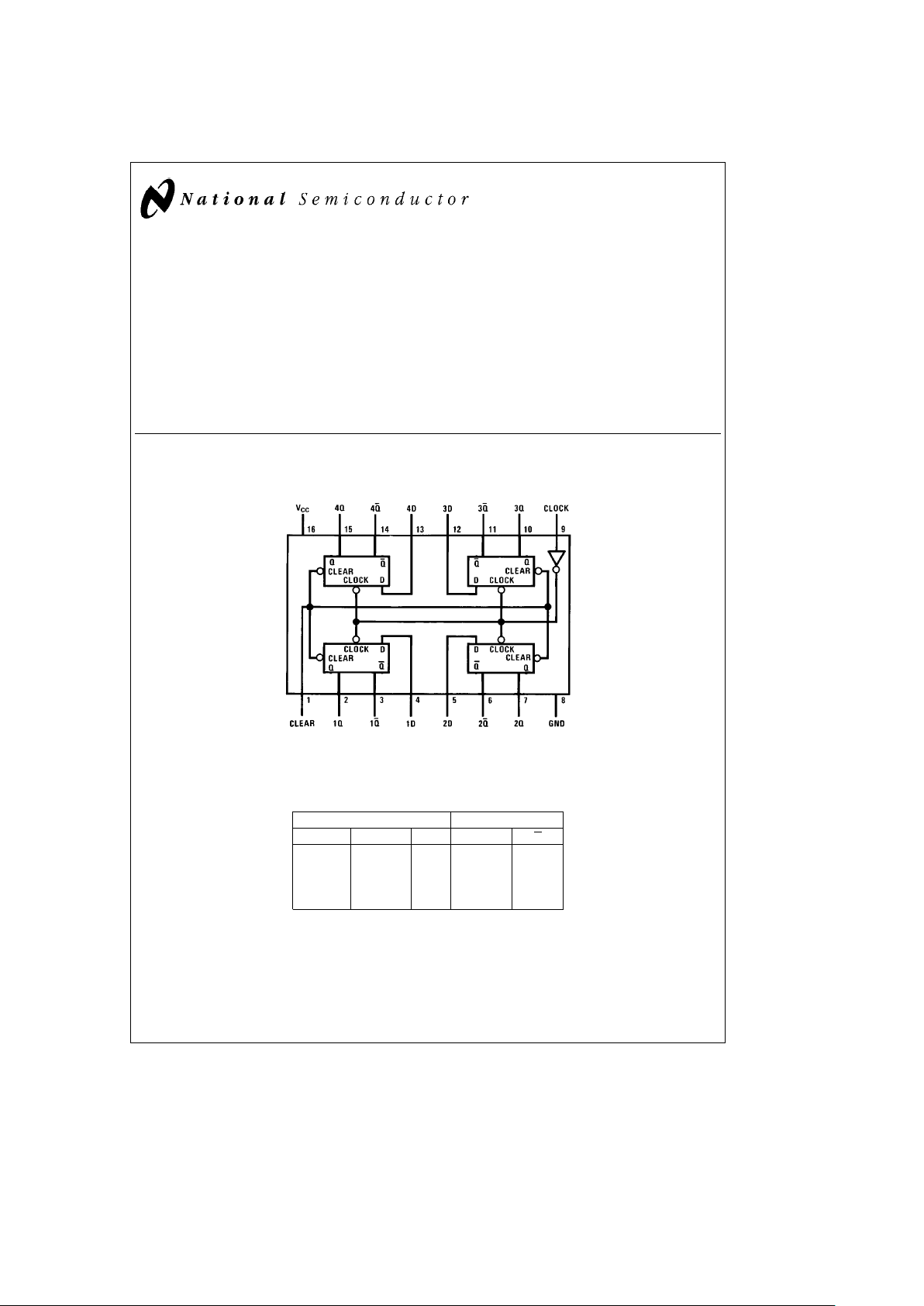
Connection Diagram & Truth Table
Dual-In-Line Package
TL/F/5900– 1
Top View
Order Number MM54C175 or MM74C175
Each Flip-Flop
Inputs Outputs
Clear Clock D Q Q
LXXLH
H
u
HH L
H
u
LL H
HHXNCNC
HLXNCNC
H
e
High level
L
e
Low level
X
e
Irrelevant
u
e
Transition from low to high level
NC
e
No change
C
1995 National Semiconductor Corporation RRD-B30M105/Printed in U. S. A.

Absolute Maximum Ratings (Note 1)
If Military/Aerospace specified devices are required,
please contact the National Semiconductor Sales
Office/Distributors for availability and specifications.
Voltage at Any Pin
b
0.3V to V
CC
a
0.3V
Operating Temperature Range
MM54C175
b
55§Ctoa125§C
MM74C175
b
40§Ctoa85§C
Storage Temperature Range
b
65§Ctoa150§C
Power Dissipation (PD)
Dual-In-Line 700 mW
Small Outline 500 mW
Operating V
CC
Range 3V to 15V
Absolute Maximum V
CC
18V
Lead Temperature
(Soldering, 10 seconds) 260
§
C
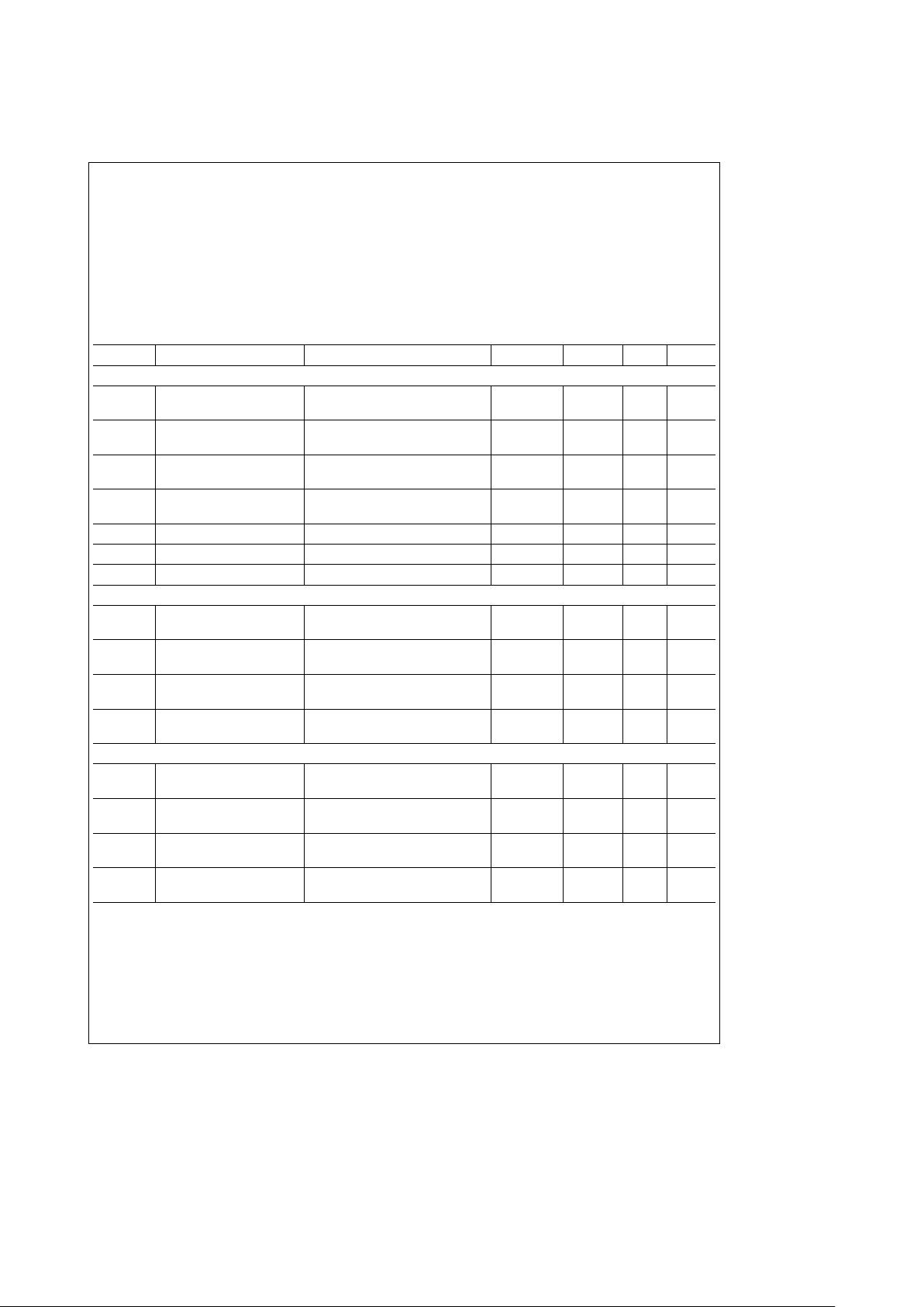
DC Electrical Characteristics Min/Max limits apply across temperature range unless otherwise specified
Symbol Parameter Conditions Min Typ Max Units
CMOS TO CMOS
V
IN(1)
Logical ‘‘1’’ Input Voltage V
CC
e
5V 3.5 V
V
CC
e
10V 8.0 V
V
IN(0)
Logical ‘‘0’’ Input Voltage V
CC
e
5V 1.5 V
V
CC
e
10V 2.0 V
V
OUT(1)
Logical ‘‘1’’ Output Voltage V
CC
e
5V, I
O
eb
10 mA 4.5 V
V
CC
e
10V, I
O
eb
10 mA 9.0 V
V
OUT(0)
Logical ‘‘0’’ Output Voltage V
CC
e
5V, I
O
e
10 mA 0.5 V
V
CC
e
10V, I
O
e
10 mA 1.0 V
I
IN(1)
Logical ‘‘1’’ Input Current V
CC
e
15V, V
IN
e
15V 0.005 1.0 mA
I
IN(0)
Logical ‘‘0’’ Input Current V
CC
e
15V, V
IN
e
0V
b
1.0
b
0.005 mA
I
CC
Supply Current V
CC
e
15V 0.05 300 mA
CMOS/LPTTL INTERFACE
V
IN(1)
Logical ‘‘1’’ Input Voltage 54C, V
CC
e
4.5V V
CC
b
1.5 V
74C, V
CC
e
4.75V V
CC
b
1.5 V
V
IN(0)
Logical ‘‘0’’ Input Voltage 54C, V
CC
e
4.5V 0.8 V
74C, V
CC
e
4.75V 0.8 V
V
OUT(1)
Logical ‘‘1’’ Output Voltage 54C, V
CC
e
4.5V, I
O
eb
360 mA 2.4 V
74C, V
CC
e
4.75V, I
O
eb
360 mA 2.4 V
V
OUT(0)
Logical ‘‘0’’ Output Voltage 54C, V
CC
e
4.5V, I
O
e
360 mA 0.4 V
74C, V
CC
e
4.75V, I
O
e
360 mA 0.4 V
OUTPUT DRIVE (See 54C/74C Family Characteristics Data Sheet) (Short Circuit Current)
I
SOURCE
Output Source Current V
CC
e
5V, T
A
e
25§C,
b
1.75
b
3.3 mA
(P-Channel) V
OUT
e
0V
I
SOURCE
Output Source Current V
CC
e
10V, T
A
e
25§C,
b
8.0
b
15 mA
(P-Channel) V
OUT
e
0V
I
SINK
Output Sink Current V
CC
e
5V, T
A
e
25§C,
1.75 3.6 mA
(N-Channel) V
OUT
e
V
CC
I
SINK
Output Sink Current V
CC
e
10V, T
A
e
25§C,
8.0 16 mA
(N-Channel) V
OUT
e
V
CC
Note 1: ‘‘Absolute Maximum Ratings’’ are those values beyond which the safety of the device cannot be guaranteed. Except for ‘‘Operating Temperature Range’’
they are not meant to imply that the devices should be operated at these limits. The table of ‘‘Electrical Characteristics’’ provides conditions for actual device
operation.
2
 Loading...