NSC MM54C165J-MIL Datasheet

TL/F/5897
MM54C165/MM74C165 Parallel-Load 8-Bit Shift Register
December 1992
MM54C165/MM74C165
Parallel-Load 8-Bit Shift Register
General Description
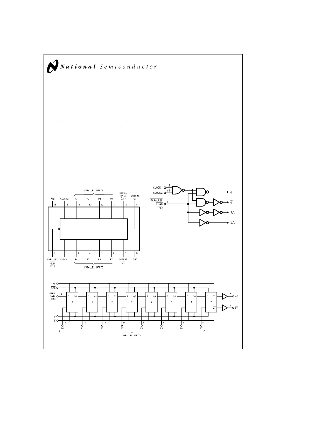
The MM54C165/MM74C165 functions as an 8-bit parallelload, serial shift register. Data is loaded into the register
independent of the state of the clock(s) when PARALLEL
LOAD (PL
) is low. Shifting is inhibited as long as PL is low.
Data is sequentially shifted from complementary outputs, Q
7
and Q7, highest-order bit (P7) first. New serial data may be
entered via the SERIAL DATA (Ds) input. Serial shifting occurs on the rising edge of CLOCK1 or CLOCK2. Clock inputs may be used separately or together for combined
clocking from independent sources. Either clock input may
be used also as an active-low clock enable. To prevent double-clocking when a clock input is used as an enable, the
enable must be changed to a high level (disabled) only while
the clock is high.
Features
Y
Wide supply voltage range 3V to 15V
Y
Guaranteed noise margin 1V
Y
High noise immunity 0.45 VCC(typ.)
Y
Low power TTL compatibility fan out of 2
driving 74L
Y
Parallel loading independent of clock
Y
Dual clock inputs
Y
Fully static operation
Connection and Block Diagrams
Dual-In-Line Package
TL/F/5897– 1
Top View
TL/F/5897– 2
Order Number MM54C165* or MM74C165*
*Please look into Section 8, Appendix D
for availability of various package types.
TL/F/5897– 3
C
1995 National Semiconductor Corporation RRD-B30M105/Printed in U. S. A.

Absolute Maximum Ratings (Note 1)
If Military/Aerospace specified devices are required,
please contact the National Semiconductor Sales
Office/Distributors for availability and specifications.
Voltage at Any Pin
b
0.3V to V
CC
a
0.3V
Operating Temperature Range
MM54C165
b
55§Ctoa125§C
MM74C165
b
40§Ctoa85§C
Storage Temperature Range
b
65§Ctoa150§C
Absolute Maximum V
CC
18V
Power Dissipation
Dual-In-Line 700 mW
Small Outline 500 mW
Operating V
CC
Range 3V to 15V
Lead Temperature (Soldering, 10 sec.) 260§C
DC Electrical Characteristics Min/Max limits apply across temperature range unless otherwise noted
Symbol Parameter Conditions Min Typ Max Units
CMOS TO CMOS
V
IN(1)
Logical ‘‘1’’ Input Voltage V
CC
e
5V 3.5 V
V
CC
e
10V 8.0 V
V
IN(0)
Logical ‘‘0’’ Input Voltage V
CC
e
5V 1.5 V
V
CC
e
10V 2.0 V
V
OUT(1)
Logical ‘‘1’’ Output Voltage V
CC
e
5V, I
O
eb
10 mA 4.5 V
V
CC
e
10V, I
O
eb
10 mA 9.0 V
V
OUT(0)
Logical ‘‘0’’ Output Voltage V
CC
e
5V, I
O
ea
10 mA 0.5 V
V
CC
e
10V, I
O
ea
10 mA 1.0 V
I
IN(1)
Logical ‘‘1’’ Input Current V
CC
e
15V, V
IN
e
15V 0.005 1.0 mA
I
IN(0)
Logical ‘‘0’’ Input Current V
CC
e
15V, V
IN
e
0V
b
1.0
b
0.005 mA
I
CC
Supply Current V
CC
e
15V 0.05 300 mA
CMOS TO LPTTL INTERFACE
V
IN(1)
Logical ‘‘1’’ Input Voltage 54C V
CC
e
4.5V V
CC
b
1.5 V
74C V
CC
e
4.75V V
CC
b
1.5 V
V
IN(0)
Logical ‘‘0’’ Input Voltage 54C V
CC
e
4.5V 0.8 V
74C V
CC
e
4.75V 0.8 V
V
OUT(1)
Logical ‘‘1’’ Output Voltage 54C V
CC
e
4.5V, I
O
eb
360 mA 2.4 V
74C V
CC
e
4.75V, I
O
eb
360 mA 2.4 V
V
OUT(0)
Logical ‘‘0’’ Output Voltage 54C V
CC
e
4.5V, I
O
e
360 mA 0.4 V
74C V
CC
e
4.75V, I
O
e
360 mA 0.4 V
OUTPUT DRIVE (See 54C/74C Family Characteristics Data Sheet) (short circuit current)
I
SOURCE
Output Source Current V
CC
e
5V
b
1.75
b
3.3 mA
(P-Channel) T
A
e
25§C, V
OUT
e
0V
I
SOURCE
Output Source Current V
CC
e
10V
b
8.0
b
15 mA
(P-Channel) T
A
e
25§C, V
OUT
e
0V
I
SINK
Output Sink Current V
CC
e
5V
1.75 3.6 mA
(N-Channel) T
A
e
25§C, V
OUT
e
V
CC
I
SINK
Output Sink Current V
CC
e
10V
8.0 16 mA
(N-Channel) T
A
e
25§C, V
OUT
e
V
CC
Note 1: ‘‘Absolute Maximum Ratings’’ are those values beyond which the safety of the device cannot be guaranteed. Except for ‘‘Operating Temperature Range’’
they are not meant to imply that the devices should be operated at these limits. The table of ‘‘Electrical Characteristics’’ provides conditions for actual device
operation.
2
 Loading...