NSC MM145453V Datasheet

MM145453
Liquid Crystal Display Driver
MM145453 Liquid Crystal Display Driver
December 1999
General Description
The MM145453 is a monolithic integrated circuit utilizing
CMOS metal gate, low threshold enhancement mode devices. The chip can drive up to 33LCDsegmentsand can be
paralleled to increase this number. The chip is capable of
driving a 4
between the display and the data source.
The MM145453 stores display data in latches after it is
clocked in, and holds the data until new display data is received.
The MM145453 is available in a molded 44 pin surface
mount PLCC package. The MM145453 is pin out and functionally compatible with the MC145453.
1
⁄2digit 7-segment display with minimal interface
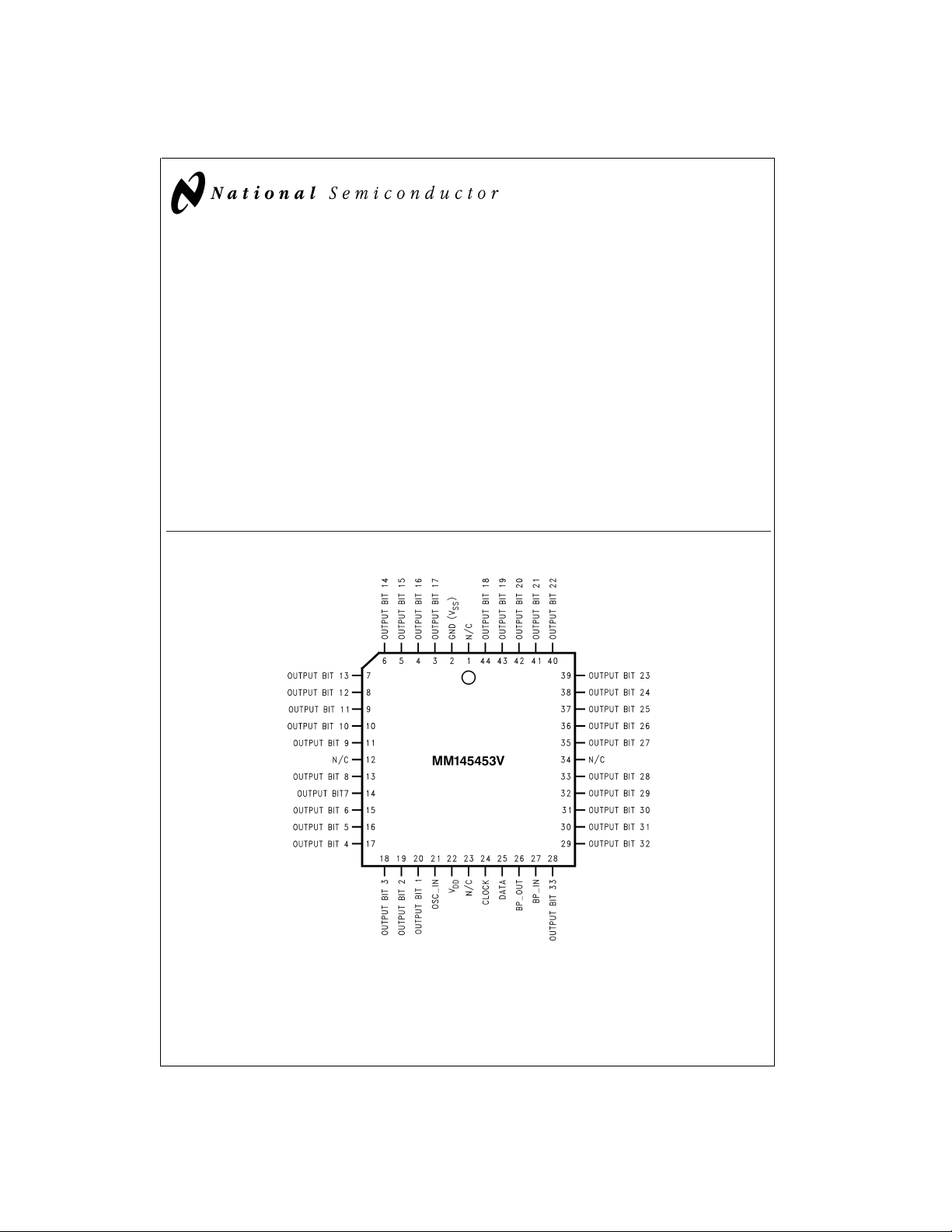
Connection Diagram
Features
n Serial Data Input
n Wide Power Supply operation
n TTL Compatibility
n Up to 33 LCD Segments
n Alphanumeric or Bar Graph capability
n Cascaded operation capability
n Pin Compatible with MC145453
Applications
n COPS™or microprocessor displays
n Industrial control indicator
n Digital clock, thermometer, counter, voltmeter
n Instrumentation displays
n Remote displays
DS101283-1
Top View
Order Number MM145453V
See NS Package Number V44A
© 1999 National Semiconductor Corporation DS101283 www.national.com

Absolute Maximum Ratings (Note 1)
If Military/Aerospace specified devices are required,
please contact the National Semiconductor Sales Office/
MM145453
Distributors for availability and specifications.
Voltage at Any Pin,
Referenced to Gnd
Storage Temperature -65˚C to +150˚C
Power Dissipation at 25˚C 350mW
Power Dissipation at 70˚C 300mW
-0.3V to +10V
Junction Temperature +150˚C
Lead Temperature
300˚C
(Soldering, 10s)
Recommended Operating
Conditions
V
DD
Operating Temperature 0˚C to 70˚C
3V to 10V
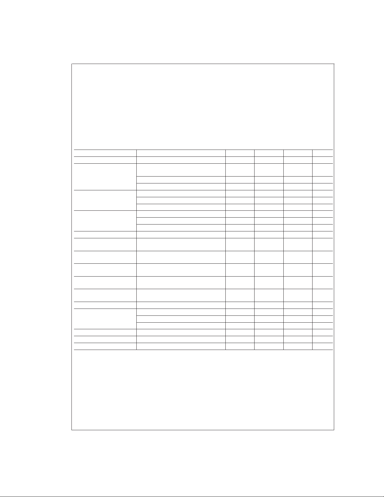
Electrical Characteristics
The following specifications apply for TAwithin operation range, V
=
3.0V to 10V, V
DD
Parameter Conditions Min Typical Max Units
Supply Voltage, V
Average Supply Current, I
Input Logical ’0’ Voltage, V
Input Logical ’1’ Voltage, V
Segment Sink Current, I
Segment Source Current,
I
OH
Backplane Out Sink Current,
I
OL
Backplane Out Source
Current, I
Segment Output Offset
DD
OH
All Outputs Open, Clock=Gnd,
DD
Data=Gnd,OSC=Gnd, BP_IN 32Hz
=5V 10 µA
V
DD
V
= 10V 40 µA
DD
ILVDD
IHVDD
OL
= 3V 0.4 V
V
= 5V 0.8 V
DD
V
= 10V 0.8 V
DD
= 3V 2.0 V
V
= 5V 2.0 V
DD
V
= 10V 8.0 V
DD
VDD= 3V, V
VDD= 3V, V
VDD= 3V, V
VDD= 3V, V
= 0.3V -20 -40 µA
OUT
= 2.7V
OUT
= 0.3V
OUT
= 2.7V
OUT
Segment Load = 250pF (Note 2)
Voltage
Backplane Output Offset
Backplane Load = 8750pF (Note 2)
Voltage
Backplane Out Frequency R
Clock Input Frequency,
f
CLOCK
= 50kΩ,C
OSC_IN
VDD= 3V (Notes 2, 3) 500 kHz
V
= 5V (Note 2) 750 kHz
DD
V
= 10V (Note 2) 1.0 MHz
DD
= 0.01µF 75 Hz
OSC_IN
Clock Input Duty Cycle 40 60
Data Input Set-Up Time, t
Data Input Hold Time, t
Note 1: “Absolute Maximum Ratings” are those values beyond which the safety of the device cannot be guaranteed. They are not meant to imply that the devices
should be operated at these limits. The table of “Electrical Characteristics” specifies conditions of device operation.
Note 2: This parameter is guaranteed (but not production tested) over the operating temperature range and the operating supply voltage range. Not to be used in
Q.A. testing.
Note 3: AC input waveform for test purposes: t
Note 4: Clock input rise time (t
DS
DH
≤ 20ns, tf≤ 20ns, f
) and fall time (tf) must not exceed 300ns
r
r
=
500kHz, Duty Cycle = 50
CLOCK
%
=
0V, unless otherwise specified.
SS
310V
20 40 µA
-320 -500 µA
320 500 µA
+/-50 mV
+/-50 mV
300 ns
300 ns
±
%
10
%
www.national.com 2
 Loading...