NSC MF6CWMX-50, MF6CWM-50, MF6CWM-100 Datasheet
MF6
6th Order Switched Capacitor Butterworth Lowpass
Filter
General Description
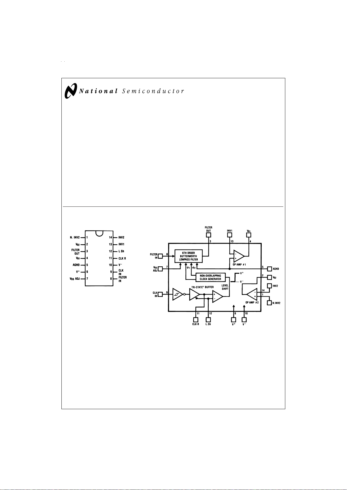
The MF6 is a versatile easy to use, precision 6th order Butterworth lowpass active filter. Switched capacitor techniques
eliminate external component requirements and allow a
clock tunable cutoff frequency. The ratio of the clock frequency to the lowpass cutoff frequency is internally set to 50
to 1 (MF6-50) or 100 to 1 (MF6-100). A Schmitt trigger clock
input stage allows two clocking options, either self-clocking
(via an external resistor and capacitor) for stand-alone applications, or an external TTL or CMOS logic compatible clock
can be used for tighter cutoff frequency control. The maximally flat passband frequency response together with a DC
gain of 1 V/V allows cascading MF6 sections for higher order
filtering. In addition to the filter, two independent CMOS op
amps are included on the die and are useful for any general
signal conditioning applications.
Features
n No external components
n Cutoff frequency accuracy of
±
0.3%typical
n Cutoff frequency range of 0.1 Hz to 20 kHz
n Two uncommitted op amps available
n 5V to 14V total supply voltage
n Cutoff frequency set by external or internal clock
Block and Connection Diagrams
TRI-STATE®is a registered trademark of National Semiconductor Corporation.
All Packages
DS005065-2
Top View
Order Number MF6CWM-50
or MF6CWM-100
See NS Package Number M14B
DS005065-1
June 1999
MF6 6th Order Switched Capacitor Butterworth Lowpass Filter
© 1999 National Semiconductor Corporation DS005065 www.national.com
Absolute Maximum Ratings (Note 11)
If Military/Aerospace specified devices are required,
please contact the National Semiconductor Sales Office/
Distributors for availability and specifications.
Supply Voltage 14V
Voltage at Any Pin V
−
− 0.2V, V++ 0.2V
Input Current at Any Pin (Note 13) 5 mA
Package Input Current (Note 13) 20 mA
Power Dissipation (Note 14) 500 mW
Storage Temperature −65˚C to +150˚C
ESD Susceptibility (Note 12) 800V
Soldering Information
Vapor Phase (60 sec.) 215˚C
Infrared (15 sec.) 220˚C
See AN-450 “Surface Mounting Methods and Their Effect
on Product Reliability” (Appendix D) for other methods of
soldering surface mount devices.
Operating Ratings (Note 11)
Temperature Range T
MIN
≤ TA≤ T
MAX
MF6CWM-50, MF6CWM-100 0˚C ≤ TA≤ +70˚C
Supply Voltage (V
S
=
V
+−V−
) 5Vto14V
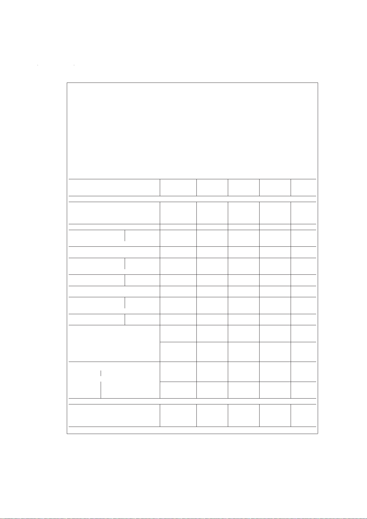
Filter Electrical Characteristics
The following specifications apply for f
CLK
≤ 250 kHz (Note 3) unless otherwise specified. Boldface limits apply for T
MIN
to T
MAX
; all other limits T
A
=
T
J
=
25˚C.
Parameter Conditions Typical Tested Design Units
(Note 8) Limit Limit
(Note 9) (Note 10)
V
+
=
+5V, V
−
=
−5V
f
c
, Cutoff MF6-50 Min 0.1
Frequency Max 20k Hz
Range MF6-100 Min 0.1
(Note 1) Max 10k
Total Supply Current f
CLK
=
250 kHz 4.0 6.0 8.5 mA
Maximum Clock Filter Output 30 mV
Feedthrough Op Amp 1 Out 25 (peak-to-
Op Amp 2 Out 20 peak)
H
o
,R
source
0.0
±
0.30
±
0.30 dB
DC Gain ≤ 2kΩ
f
CLK/fc
MF6-50 49.27±0.3
%
49.27±1
%
49.27±1
%
Clock to Cutoff MF6-100 98.97
±
0.3
%
98.97±1
%
98.97±1
%
Frequency Ratio
DC MF6-50 −200 mV
Offset Voltage MF6-100 −400
Minimum Output R
L
=
10 kΩ +4.0 +3.5 +3.5 V
Voltage Swing −4.1 −3.8 −3.5
Maximum Output Source 50
Short Circuit Sink 1.5 mA
Current (Note 6)
Dynamic Range MF6-50 83 dB
(Note 2) MF6-100 81
Additional MF6-50 f
CLK
=
250 kHz
Magnitude f=6000 Hz −9.47 −9.47
±
0.6 −9.47±0.75 dB
Response Test f=4500 Hz −0.92 −0.92
±
0.6 −0.92±0.4
Points (Note
4)
MF6-100 f
CLK
=
250 kHz
f=3000 Hz −9.48 −9.48
±
0.3 −9.48±0.75 dB
f=2250 Hz −0.97 −0.97
±
0.3 −0.97±0.4
Attenuation
Rate
MF6-50 f
CLK
=
250 kHz
dB/
f
1
=
6000 Hz −36 −36 octave
f
2
=
8000 Hz
MF6-100 f
CLK
=
250 kHz dB/
f
1
=
3000 Hz −36 −36 octave
f
2
=
4000 Hz
V
+
=
+2.5V, V
−
=
−2.5V
f
c
, Cutoff MF6-50 Min 0.1
Frequency Max 10k Hz
Range MF6-100 Min 0.1
(Note 1) Max 5k
www.national.com 2
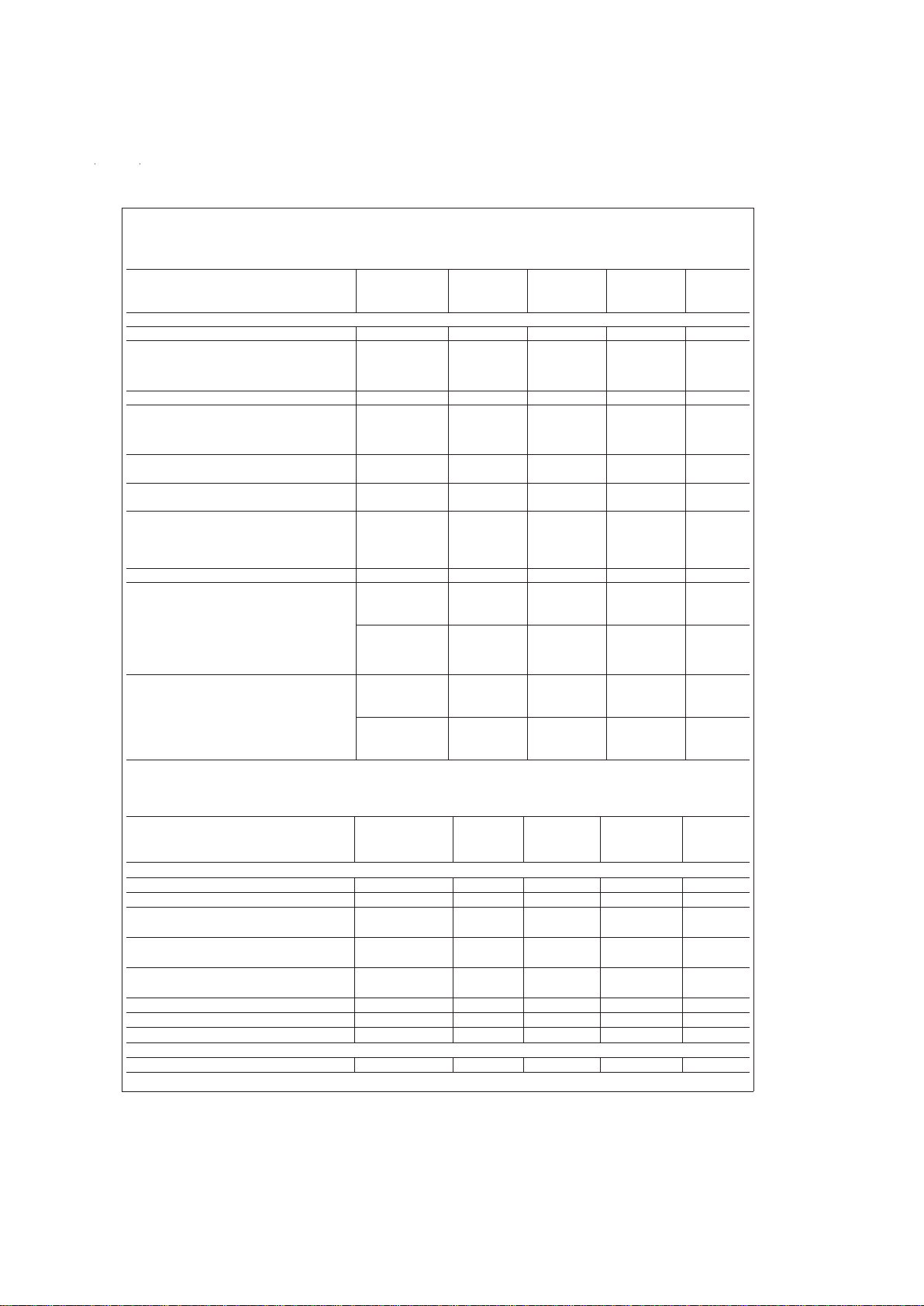
Filter Electrical Characteristics (Continued)
The following specifications apply for f
CLK
≤ 250 kHz (Note 3) unless otherwise specified. Boldface limits apply for T
MIN
to T
MAX
; all other limits T
A
=
T
J
=
25˚C.
Parameter Conditions Typical Tested Design Units
(Note 8) Limit Limit
(Note 9) (Note 10)
V
+
=
+2.5V, V
−
=
−2.5V
Total Supply Current f
CLK
=
250 kHz 2.5 4.0 4.0 mA
Maximum
Clock
Filter Output 20 mV
Feedthrough Op Amp 1 Out 15 (peak-to-
Op Amp 2 Out 10 peak)
H
o
, DC Gain R
source
≤2kΩ 0.0
±
0.30
±
0.30 dB
f
CLK/fc
, Clock to
Cutoff
Frequency
MF6-50 49.10
±
0.3
%
49.10±2
%
49.10±3
%
Ratio MF6-100 98.65
±
0.3
%
98.65±2
%
98.65±2.25
%
DC MF6-50 −200 mV
Offset Voltage MF6-100 −400
Minimum Output R
L
=
10 kΩ +1.5 +1.0 +1.0 V
Voltage Swing −2.2 −1.7 −1.5
Maximum
Output
Source
28
Short Circuit Sink 0.5 mA
Current
(Note 6)
Dynamic Range (Note 2) 77 dB
Additional MF6-50 f
CLK
=
250 kHz
Magnitude f=6000 Hz −9.54 −9.54
±
0.6 −9.54±0.75 dB
Response Test f=4500 Hz −0.96 −0.96
±
0.3 −0.96±0.4
Points (Note
4)
MF6-100 f
CLK
=
250 kHz
f=3000 Hz −9.67 −9.67
±
0.6 −9.67±0.75 dB
f=2250 Hz −1.01 −1.01
±
0.3 −1.01±0.4
Attenuation MF6-50 f
CLK
=
250 kHz dB/
Rate f
1
=
6000 Hz −36 −36 octave
f
2
=
8000 Hz
MF6-100 f
CLK
=
250 kHz dB/
f
1
=
3000 Hz −36 −36 octave
f
2
=
4000 Hz
Op Amp Electrical Characteristics
Boldface limits apply for T
MIN
to T
MAX
; all other limits T
A
=
T
J
=
25˚C.
Parameter Conditions Typical Tested Design Units
(Note 8) Limit Limit
(Note 9) (Note 10)
V
+
=
+5V, V
−
=
−5V
Input Offset Voltage
±
8.0
±
20
±
20 mV
Input Bias Current 10 pA
CMRR (Op Amp
#
2 Only) V
CM1
=
1.8V, 60 55 dB
V
CM2
=
−2.2V
Output Voltage Swing R
L
=
10 kΩ +4.0 +3.8 +3.6 V
−4.5 −4.0 −4.0
Maximum Output Short Source 54 65 80
mA
Circuit Current (Note 6) Sink 2.0 4.0 6.0
Slew Rate 7.0 V/µs
DC Open Loop Gain 72 dB
Gain Bandwidth Product 1.2 MHz
V
+
=
+2.5V, V
−
=
−2.5V
Input Offset Voltage
±
8.0
±
20
±
20 mV
www.national.com3
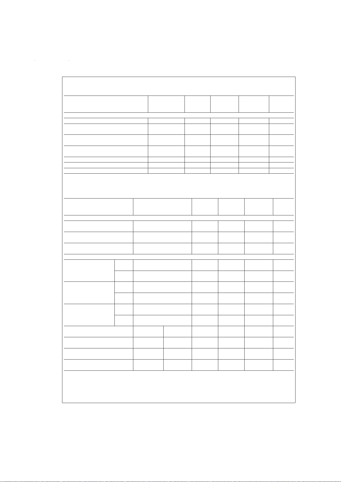
Op Amp Electrical Characteristics (Continued)
Boldface limits apply for T
MIN
to T
MAX
; all other limits T
A
=
T
J
=
25˚C.
Parameter Conditions Typical Tested Design Units
(Note 8) Limit Limit
(Note 9) (Note 10)
V
+
=
+2.5V, V
−
=
−2.5V
Input Bias Current 10 pA
CMRR (Op-Amp
#
2 Only) V
CM1
=
+0.5V, 60 55 dB
V
CM2
=
−0.9V
Output Voltage Swing R
L
=
10 kΩ +1.5 +1.3 +1.1 V
−2.2 −1.7 −1.7
Maximum Output Short Source 24 mA
Circuit Current (Note 6) Sink 1.0
Slew Rate 6.0 V/µs
DC Open Loop Gain 67 dB
Gain Bandwidth Product 1.2 MHz
Logic Input-Output Electrical Characteristics
(Note 5) The following specifications apply for V
−
=
0V unless otherwise specified. Boldface limits apply for T
MIN
to
T
MAX
; all other limits T
A
=
T
J
=
25˚C.
Parameter Conditions Typical Tested Design Units
(Note 8) Limit Limit
(Note 9) (Note 10)
TTL CLOCK INPUT, CLK R PIN (Note 7)
Maximum V
IL
, Logical “0” 0.8 0.8 V
Input Voltage
Minimum V
IH
, Logical “1” 2.0 2.0 V
Input Voltage
Maximum Leakage Current L Sh Pin at 2.0 2.0 µA
at CLK R Pin Mid- Supply
SCHMITT TRIGGER
V
T+
, Positive Going Min V
+
=
10V 7.0 6.1 6.1 V
Threshold Voltage Max 8.9 8.9
Min V
+
=
5V 3.5 3.1 3.1 V
Max 4.4 4.4
V
T−
, Negative Going Min V
+
=
10V 3.0 1.3 1.3 V
Threshold Voltage Max 3.8 3.8
Min V
+
=
5V 1.5 0.6 0.6 V
Max 1.9 1.9
Hysteresis (V
T+−VT−
) Min V
+
=
10V 4.0 2.3 2.3 V
Max 7.6 7.6
Min V
+
=
5V 2.0 1.2 1.2 V
Max 3.8 3.8
Minimum Logical “1” Output
I
o
=
−10µA
V
+
=
10V 9.0 9.0 V
Voltage (Pin 11) V
+
=
5V 4.5 4.5
Maximum Logical “0” Output
I
o
=
10µA
V
+
=
10V 1.0 1.0 V
Voltage (Pin 11) V
+
=
5V 0.5 0.5
Minimum Output Source CLK R Tied V
+
=
10V 6.0 3.0 3.0 mA
Current (Pin 11) to Ground V
+
=
5V 1.5 0.75 0.75
Maximum Output Sink CLK R Tied V
+
=
10V 5.0 2.5 2.5 mA
Current (Pin 11) to V
+
V
+
=
5V 1.3 0.65 0.65
Note 1: The cutoff frequency of the filter is defined as the frequency where the magnitude response is 3.01 dB less than the DC gain of the filter.
Note 2: For
±
5V supplies the dynamic range is referenced to 2.82 Vrms (4V peak) where the wideband noise over a 20 kHz bandwidth is typically 200 µVrms for
the MF6-50 and 250 µVrmsfortheMF6-100.For
±
2.5V supplies the dynamic range isreferencedto1.06Vrms (1.5V peak) where the widebandnoiseovera20kHz
bandwidth is typically 140 µVrms for both the MF6-50 and the MF6-100.
Note 3: The specifications for the MF6 have been given for a clock frequency (f
CLK
) of 250 kHz and less. Above this clock frequency the cutoff frequency begins to
deviate from the specified error band of
±
1.0%but the filter still maintains its magnitude characteristics. See Application Hints, Section 1.5.
www.national.com 4
Logic Input-Output Electrical Characteristics (Continued)
Note 4: Besides checking the cutoff frequency (fc) and the stopband attenuation at 2 fc, two additional frequencies are used to check the magnitude response of the
filter. The magnitudes are referenced to a DC gain of 0.0 dB.
Note 5: For simplicity all the logic levels have been referenced to V
−
=
0V and will scale accordingly for
±
5V and±2.5V supplies (except for the TTL input logic lev-
els).
Note 6: The short circuit source current is measured by forcing the output that is being tested to its maximum positive voltage swing and then shorting that output
to the negative supply. The short circuit sink current is measured by forcing the output that is being tested to its maximum negative voltage swing and then shorting
that output to the positive supply. These are the worst-case conditions.
Note 7: The MF6 is operating with symmetrical split supplies and L.Sh is tied to ground.
Note 8: Typicals are at 25˚C and represent most likely parametric norm.
Note 9: Tested limits are guaranteed to National’s AOQL (Average Outgoing Quality Level).
Note 10: Design limits are guaranteed, but not 100%tested. These limits are not used to calculate outgoing quality levels.
Note 11: Absolute Maximum Ratings indicate limits beyond which damage to the device mayoccur. DC andACelectricalspecifications do not apply when operating
the device beyond its specified conditions.
Note 12: Human body model, 100 pF discharged through a 1.5k Ω resistor.
Note 13: When the input voltage (V
IN
) at any pin exceeds the power supply rails (V
IN
<
V−or V
IN
>
V+) the absolute value of current at that pin should be limited
to 5 mA or less. The 20 mA package input current limits the number of pins that can exceed the power supply boundaries witha5mAcurrent limit to four.
Note 14: The maximum power dissipation must be derated at elevated temperatures and is dictated by T
JMAX
, θJA, and the ambient temperature, TA. The maximum
allowable power dissipation at any temperature is P
D
=
(T
JMAX−TA
)/θJAor the number given in the Absolute Maximum Ratings, whichever is lower. For this device,
T
JMAX
=
125˚C, and the typical junction-to-ambient thermal resistance is 78˚C/W. For the MF6CJ this number decreases to 62˚C/W. For MF6CWM, θ
JA
=
78˚C/W.
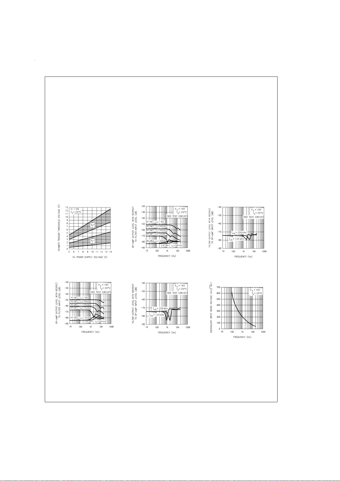
Typical Performance Characteristics
Schmitt Trigger Threshold Voltage
vs Power Supply Voltage
DS005065-40
Crosstalk from Filter
to Op-Amps (MF6-100)
DS005065-41
Crosstalk from Either Op-Amp
to Filter Output (MF6-50)
DS005065-42
Crosstalk from Filter
to Op-Amps (MF6-50)
DS005065-43
Crosstalk from Either Op-Amp to
Filter Output (MF6-100)
DS005065-44
Equivalent Input Noise
Voltage of Op-Amps
DS005065-45
www.national.com5
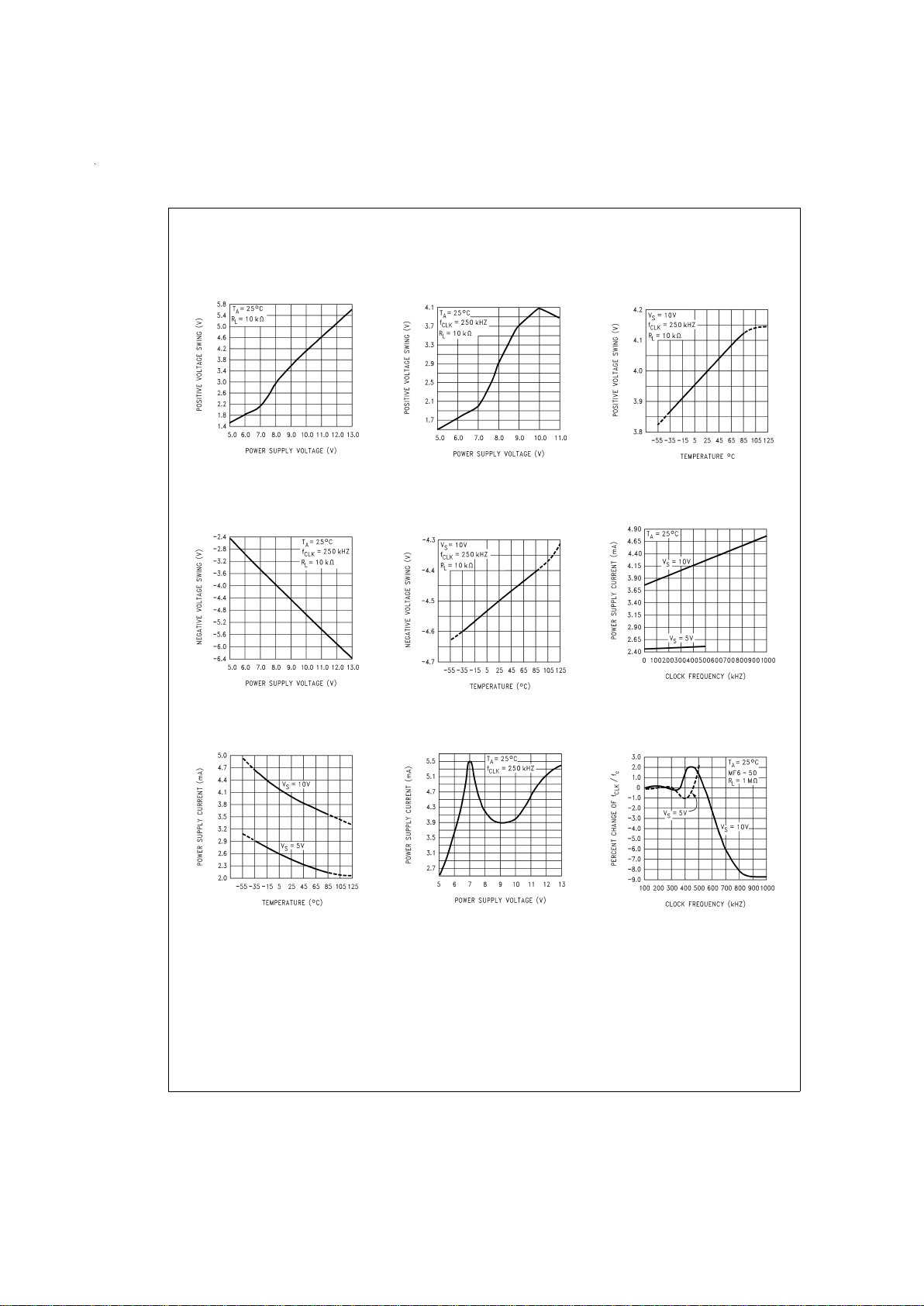
Typical Performance Characteristics (Continued)
Positive Voltage Swing vs
Power Supply Voltage
(Op Amp Output)
DS005065-46
Positive Voltage Swing vs
Power Supply Voltage
(Filter Output)
DS005065-47
Positive Voltage Swing vs
Temperature (Filter and
Op Amp Outputs)
DS005065-48
Negative Voltage Swing vs
Power Supply Voltage
(Filter and Op Amp Outputs)
DS005065-49
Negative Voltage Swing vs
Temperature (Filter and
Op Amp Outputs)
DS005065-50
Power Supply Current vs
Clock Frequency
DS005065-51
Power Supply Current
vs Temperature
DS005065-52
Power Supply Current
vs Power Supply Voltage
DS005065-53
f
CLK/fc
Deviation
vs Clock Frequency
DS005065-54
www.national.com 6
 Loading...