

Page 1
MF10
Universal Monolithic Dual Switched Capacitor Filter
General Description
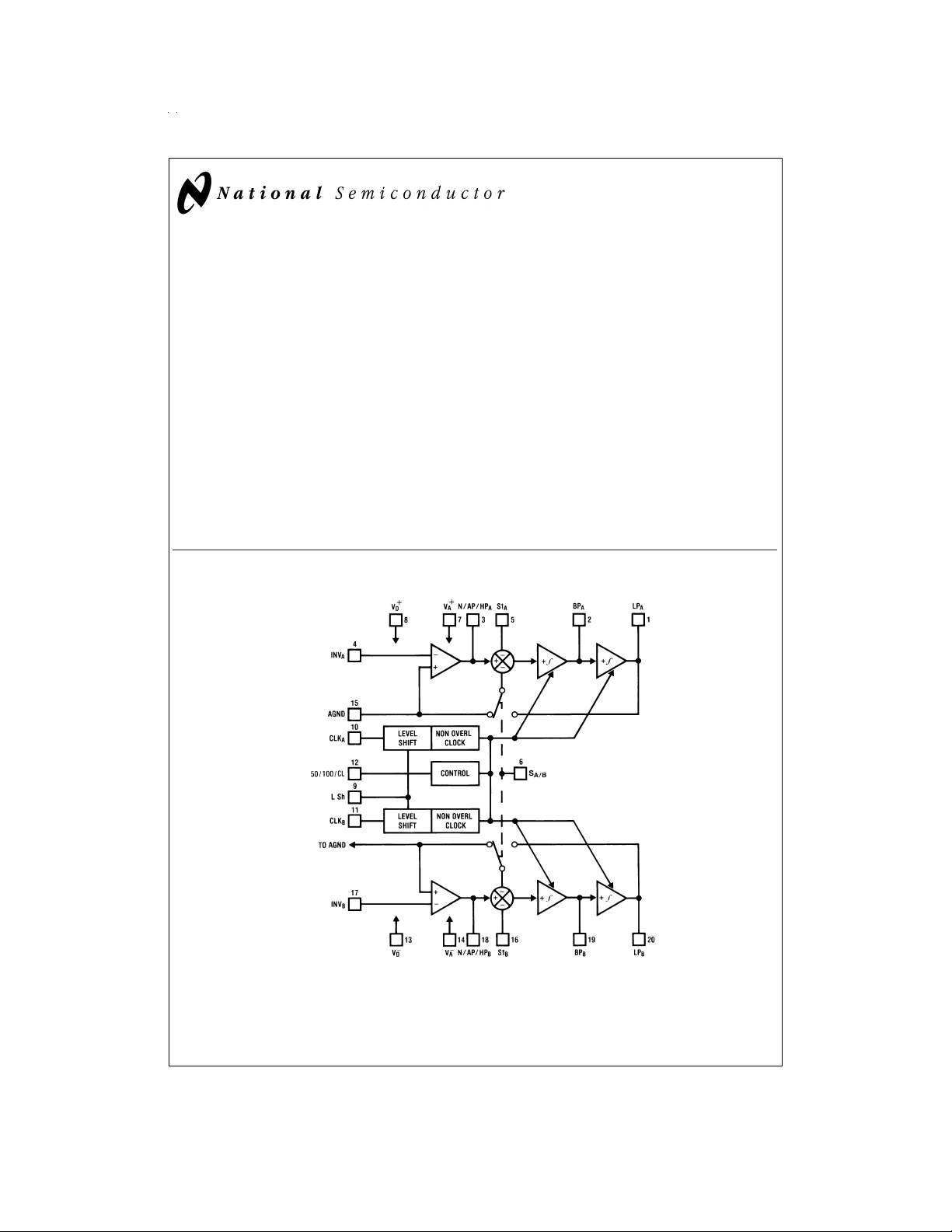
The MF10 consists of 2 independent and extremely easy to
use, general purpose CMOS active filter building blocks.
Each block, together with anexternal clock and 3 to 4 resistors, can produce various 2nd order functions. Each building
block has 3 output pins. One of the outputs can be configured to perform either an allpass, highpass or a notch function; the remaining 2 output pins perform lowpass and bandpass functions. The center frequency of the lowpass and
bandpass 2nd order functions can be either directly dependent on the clock frequency, or they can depend on both
clock frequency and external resistor ratios. The center frequency of the notch and allpass functions is directly dependent on the clock frequency, while the highpass center frequency depends on both resistor ratio and clock. Up to 4th
order functions can be performed by cascading the two 2nd
order building blocks of the MF10; higher than 4th order
functions can be obtained by cascading MF10 packages.
System Block Diagram
Any of the classical filter configurations (such as Butterworth, Bessel, Cauer and Chebyshev) can be formed.
For pin-compatible device with improved performance refer
to LMF100 datasheet.
Features
n Easy to use
n Clock to center frequency ratio accuracy
n Filter cutoff frequency stability directly dependent on
external clock quality
n Low sensitivity to external component variation
n Separate highpass (or notch or allpass), bandpass,
lowpass outputs
n f
x Q range up to 200 kHz
O
n Operation up to 30 kHz
n 20-pin 0.3" wide Dual-In-Line package
n 20-pin Surface Mount (SO) wide-body package
±
June 1999
%
0.6
MF10 Universal Monolithic Dual Switched Capacitor Filter
Package in 20 pin molded wide body surface mount and 20 pin molded DIP.
© 1999 National Semiconductor Corporation DS010399 www.national.com
DS010399-1
Page 2
Absolute Maximum Ratings (Note 1)
If Military/Aerospace specified devices are required,
please contact the National Semiconductor Sales Office/
Distributors for availability and specifications.
Supply Voltage (V
Voltage at Any Pin V
Input Current at Any Pin (Note 2) 5 mA
Package Input Current (Note 2) 20 mA
Power Dissipation (Note 3) 500 mW
Storage Temperature 150˚C
+−V−
) 14V
V
+
+ 0.3V
−
− 0.3V
SO Package:
Vapor Phase (60 Sec.) 215˚C
Infrared (15 Sec.) 220˚C
See AN-450 “Surface Mounting Methods and Their Effect
on Product Reliability” (Appendix D) for other methods of
soldering surface mount devices.
Operating Ratings (Note 1)
Temperature Range T
MF10ACN, MF10CCN 0˚C ≤ TA≤ 70˚C
MF10CCWM 0˚C ≤ T
MIN
≤ TA≤ T
≤ 70˚C
A
ESD Susceptability (Note 11) 2000V
Soldering Information
N Package: 10 sec 260˚C
Electrical Characteristics
+
=
V
+5.00V and V
=
25˚C.
Symbol Parameter Conditions Typical Tested Design Units
+−V−
V
I
S
f
O
f
CLK
f
CLK/fO
f
CLK/fO
H
OLP
V
OS1
V
OS2
V
OS3
V
OS2
V
OS3
V
OUT
GBW Op Amp Gain BW Product 2.5 MHz
SR Op Amp Slew Rate 7 V/µs
−
=
−5.00V unless otherwise specified. Boldface limits apply for T
Supply Voltage Min 9 V
Maximum Supply Clock Applied to Pins 10 & 11 8 12 12 mA
Current No Input Signal
Center Frequency Min fOxQ<200 kHz 0.1 0.2 Hz
Range Max 30 20 kHz
Clock Frequency Min 5.0 10 Hz
Range Max 1.5 1.0 MHz
50:1 Clock to
Center Frequency
Ratio Deviation
100:1 Clock to
Center Frequency
Ratio Deviation
Clock Feedthrough Q=10
Q Error (MAX) Q=10 V
(Note 4) Mode 1 f
DC Lowpass Gain Mode 1 R1=R2=10k 0
DC Offset Voltage (Note 5)
DC Offset Voltage Min V
(Note 5) Max (f
DC Offset Voltage Min V
(Note 5) Max (f
DC Offset Voltage V
(Note 5) (f
DC Offset Voltage V
(Note 5) (f
Minimum Output BP, LP Pins R
Voltage Swing N/AP/HP Pin R
Max 14 V
=
MF10C Q=10
MF10C Q=10
Min V
Max (f
Mode 1
Mode 1
Mode 1
pin12
CLK/fO
pin12
CLK/fO
pin12
CLK/fO
pin12
CLK/fO
V
pin12
(f
CLK/fO
pin12
CLK/fO
=
L
=
L
=
+5V S
=
50) −85 −85
=
+5V S
=
50)
=
+5V All Modes −70 −100 −100 mV
=
50) −20 −20
=
0V S
=
100)
=
0V S
=
100)
=
0V All Modes −140 mV
=
100)
5k
3.5k
5V
V
pin12
=
f
250 KHz
CLK
=
0V
V
pin12
=
f
500 kHz
CLK
=
5V
pin12
=
250 kHz
CLK
=
V
0V
pin12
=
f
500 kHz
CLK
+
=
V
A/B
−
=
V
A/B
+
=
V
A/B
−
=
V
A/B
to T
MIN
(Note 8) Limit Limit
±
0.2
±
0.2
10 mV
±
2
±
2
±
5.0
−150 −185 −185 mV
−70 mV
−300 mV
−140 mV
±
4.25
±
4.25
; all other limits T
MAX
MF10ACN, MF10CCN,
MF10CCWM
(Note 9) (Note 10)
±
1.5
±
1.5
±
6
±
6
±
0.2
±
20
±
3.8
±
3.8
=
A
±
1.5
±
1.5
±
6
±
6
±
0.2 dB
±
20 mV
±
3.8 V
±
3.8 V
T
MAX
J
%
%
%
%
www.national.com 2
Page 3
Electrical Characteristics (Continued)
+
=
V
+5.00V and V
=
25˚C.
Symbol Parameter Conditions Typical Tested Design Units
I
SC
−
Dynamic
Range(Note 6)
Maximum Output
Short
Circuit Current
(Note 7)
=
−5.00V unless otherwise specified. Boldface limits apply for T
=
V
+5V
pin12
=
(f
50)
CLK/fO
=
V
0V
pin12
=
(f
100)
Source 20 mA
Sink 3.0 mA
CLK/fO
to T
MIN
(Note 8) Limit Limit
83 dB
80 dB
; all other limits T
MAX
MF10ACN, MF10CCN,
MF10CCWM
(Note 9) (Note 10)
A
=
T
J
Logic Input Characteristics
=
Boldface limits apply for T
MIN
to T
MAX
; all other limits T
Parameter Conditions Typical Tested Design Units
+
−
=
=
=
(T
+5V, V
=
0V −3.0 −3.0 V
LSh
+
LSh
+
LSh
+
LSh
JMAX−TA
−
=
+10V, V
=
+5V +2.0 +2.0 V
−
=
=
+5V, V
=
0V +0.8 +0.8 V
−
=
+10V, V
=
+5V +0.8 +0.8 V
)/θJAor the number given in the Absolute Maximum Ratings, whichever is lower. For this device,
CMOS Clock Min Logical “1” V
Input Voltage Max Logical “0” V
Min Logical “1” V
Max Logical “0” V
TTL Clock Min Logical “1” V
Input Voltage Max Logical “0” V
Min Logical “1” V
Max Logical “0” V
Note 1: Absolute Maximum Ratings indicate limits beyond which damage to the device may occur. DC and AC electrical specifications do not apply when operating
the device beyond its specified operating conditions.
Note 2: When the input voltage (V
to 5 mA or less. The 20 mA package input current limits the number of pins that can exceed the power supply boundaries witha5mAcurrent limit to four.
Note 3: The maximum power dissipation must be derated at elevated temperatures and is dictated by T
allowable power dissipation at any temperature is P
=
T
125˚C, and the typical junction-to-ambient thermal resistance of the MF10ACN/CCN when board mounted is 55˚C/W. For the MF10AJ/CCJ, this number in-
JMAX
creases to 95˚C/W and for the MF10ACWM/CCWM this number is 66˚C/W.
Note 4: The accuracy of the Q value is a function of the center frequency (f
istics”.
Note 5: V
Note 6: For
the MF10 with a 50:1 CLK ratio and 280 µV rms for the MF10 with a 100:1 CLK ratio.
Note 7: The short circuit source current is measured by forcing the output that is being tested to its maximum positive voltage swing and then shorting that output
to the negative supply. The short circuit sink current is measured by forcing the output that is being tested to its maximum negative voltage swing and then shorting
that output to the positive supply. These are the worst case conditions.
Note 8: Typicals are at 25˚C and represent most likely parametric norm.
Note 9: Tested limits are guaranteed to National’s AOQL (Average Outgoing Quality Level).
Note 10: Design limits are guaranteed but not 100%tested. These limits are not used to calculate outgoing quality levels.
Note 11: Human body model, 100 pF discharged through a 1.5 kΩ resistor.
, and V
OS1,VOS2
±
5V supplies the dynamic range is referenced to 2.82V rms (4V peak) where the wideband noise over a 20 kHz bandwidth is typically 200 µV rms for
) at any pin exceeds the power supply rails (V
IN
D
refer to the internal offsets as discussed in the Applications Information Section 3.4.
OS3
=
T
25˚C
A
J
MF10ACN, MF10CCN,
MF10CCWM
(Note 8) Limit Limit
(Note 9) (Note 10)
−5V, +3.0 +3.0 V
=
0V, +8.0 +8.0 V
−5V, +2.0 +2.0 V
=
0V, +2.0 +2.0 V
<
IN
). This is illustrated in the curves under the heading “Typical Performance Character-
O
V−or V
>
V+) the absolute value of current at that pin should be limited
IN
, θJA, and the ambient temperature, TA. The maximum
JMAX
www.national.com3
Page 4
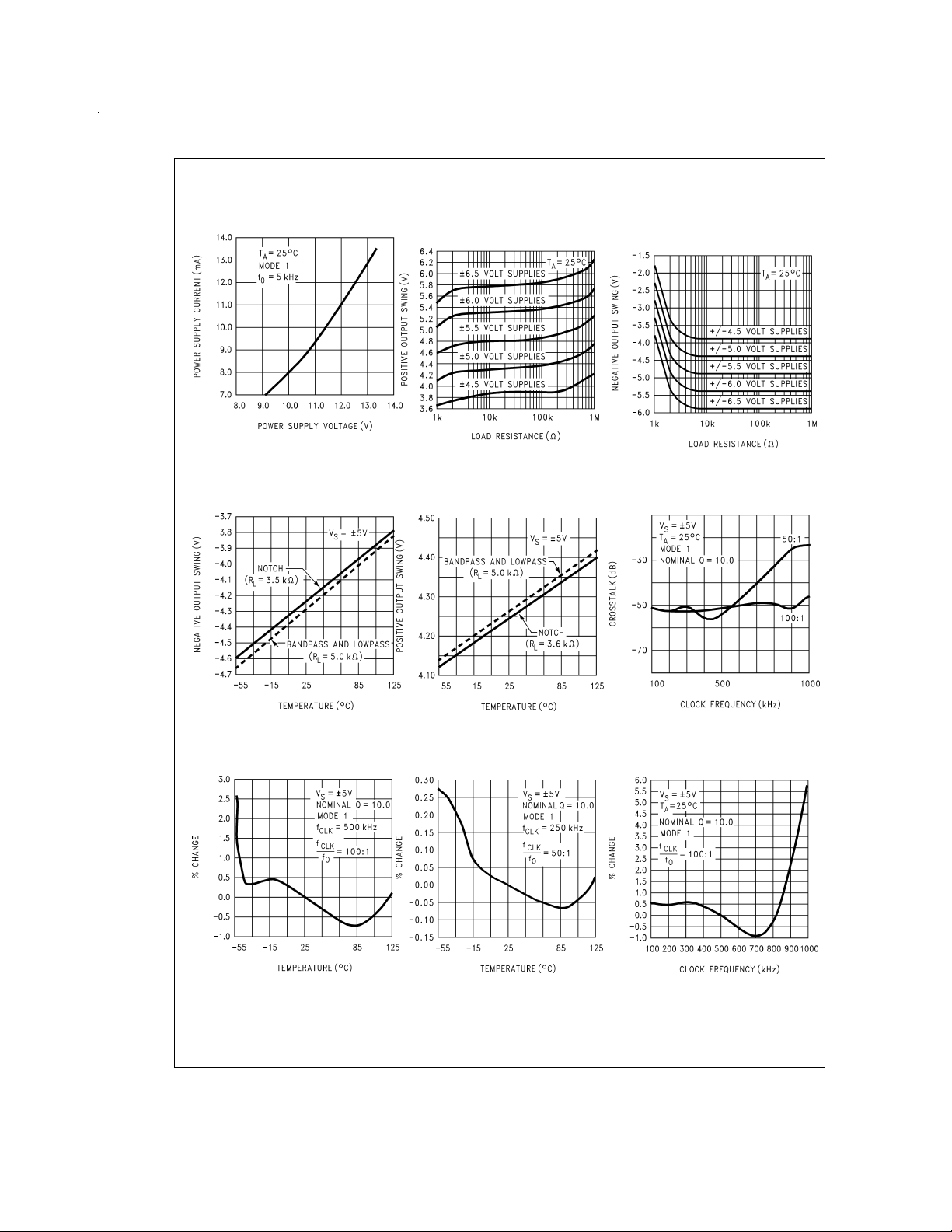
Typical Performance Characteristics
Power Supply Current
vs Power Supply Voltage
Negative Output
Swing vs Temperature
Positive Output Voltage Swing
vs Load Resistance
(N/AP/HP Output)
DS010399-34
Positive Output Swing
vs Temperature
DS010399-35
Negative Output Voltage
Swing vs Load
Resistance (N/AP/HP Output)
DS010399-36
Crosstalk vs Clock
Frequency
DS010399-37
Q Deviation vs
Temperature
www.national.com 4
Q Deviation vs
Temperature
DS010399-40
DS010399-38
DS010399-41
DS010399-39
Q Deviation vs
Clock Frequency
DS010399-42
Page 5
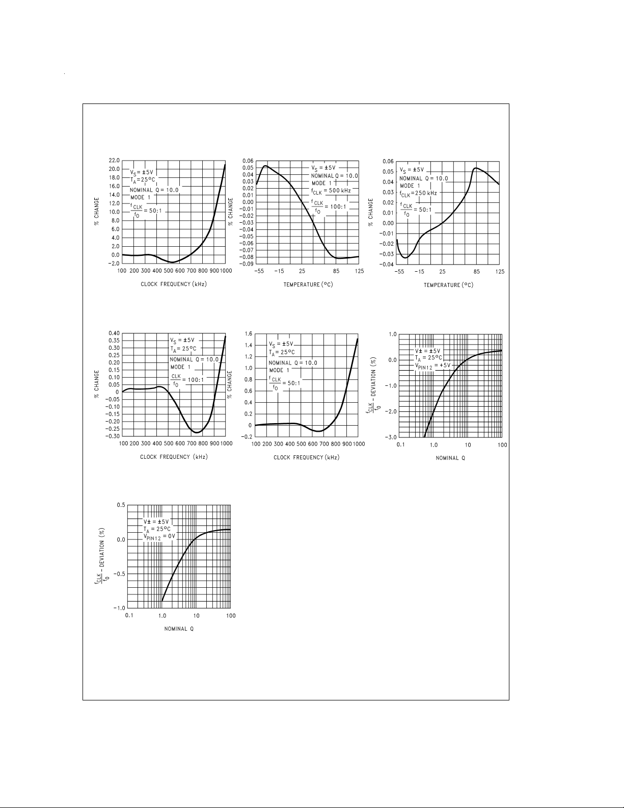
Typical Performance Characteristics (Continued)
Q Deviation vs
Clock Frequency
f
Deviation
CLK/fO
vs Clock Frequency
f
CLK/fO
vs Temperature
DS010399-43
f
CLK/fO
vs Clock Frequency
Deviation
Deviation
DS010399-44
f
Deviation
CLK/fO
vs Temperature
Deviation of f
vs Nominal Q
DS010399-45
CLK/fO
Deviation of f
vs Nominal Q
CLK/fO
DS010399-46
DS010399-49
DS010399-47
DS010399-48
www.national.com5
Page 6
Pin Descriptions
LP(1,20), BP(2,19),
N/AP/HP(3,18)
INV(4,17) The inverting input of the summing
S1(5,16) S1 is a signal input pin used in the all-
S
(6) This pin activates a switch that con-
A/B
+
V
V
+
(7),V
(8) Analog positive supply and digital posi-
A
D
−
−
(14), V
A
D
LSh(9) Level shift pin; it accommodates vari-
CLKA(10),
CLKB(11)
The second order lowpass, bandpass
and notch/allpass/highpass outputs.
These outputs can typically sink 1.5
mAand source 3 mA. Each output typically swings to within 1V of each supply.
op-amp of each filter. These are high
impedance inputs, but the
non-inverting input is internally tied to
AGND, making INV
like summing junctions (low imped-
and INVBbehave
A
ance, current inputs).
pass filter configurations (see modes 4
and 5). The pin should be driven with a
source impedance of less than 1 kΩ.If
S1 is not driven with a signal it should
be tied to AGND (mid-supply).
nects one of the inputs of each filter’s
second summer to either AGND (S
tied to V−) or to the lowpass (LP) output (S
flexibility needed for configuring the fil-
tied to V+). This offers the
A/B
A/B
ter in its various modes of operation.
tive supply. These pins are internally
connected through the IC substrate
and therefore V
derived from the same power supply
A
+
and V
+
should be
D
source. They have been brought out
separately so they can be bypassed by
separate capacitors, if desired. They
can be externally tied together and bypassed by a single capacitor.
(13) Analog and digital negative supplies.
The same comments as for V
+
V
apply here.
D
+
and
A
ous clock levels with dual or single
supply operation. With dual
±
5V supplies, the MF10 can be driven with
CMOS clock levels (
±
5V) and the LSh
pin should be tied to the system
ground. If the same supplies as above
are used but only TTL clock levels, derived from 0V to +5V supply, are available, the LSh pin should be tied to the
system ground. For single supply operation (0V and +10V) the V
−
V
pins should be connected to the
D
system ground, the AGND pin should
A
be biased at +5V and the LSh pin
should also be tied to the system
ground for TTL clock levels. LSh
should be biased at +5V for CMOS
clock levels in 10V single-supply applications.
Clock inputs for each switched capacitor filter building block. They should
both be of the same level (TTL or
CMOS). The level shift (LSh) pin description discusses how to accommo-
date their levels. The duty cycle of the
clock should be close to 50%especially when clock frequencies above
200 kHz are used. This allows the
maximum time for the internal
op-amps to settle, which yields optimum filter operation.
50/100/CL(12) By tying this pin high a 50:1
clock-to-filter-center-frequency ratio is
obtained. Tying this pin at mid-supplies
(i.e. analog ground with dual supplies)
allows the filter to operate at a 100:1
clock-to-center-frequency ratio. When
the pin is tied low (i.e., negative supply
with dual supplies), a simple current
limiting circuit is triggered to limit the
overall supply current down to about
2.5 mA. The filtering action is then
aborted.
AGND(15) This is the analog ground pin. This pin
should be connected to the system
ground for dual supply operation or biased to mid-supply for single supply
operation. For a further discussion of
mid-supply biasing techniques see the
Applications Information (Section 3.2).
For optimum filter performance a
“clean” ground must be provided.
1.0 Definition of Terms
f
: the frequency of the external clock signal applied to pin
CLK
10 or 11.
f
: center frequency of the second order function complex
O
pole pair. f
MF10, and is the frequency of maximum bandpass gain.
(
Figure 1
f
notch
notch outputs.
f
: the center frequency of the second order complex zero
z
pair, if any. If f
observed as the frequency of a notch at the allpass output.
(
Figure 10
Q: “quality factor” of the 2nd order filter. Q is measured at the
bandpass outputs of the MF10 and is equal to f
the −3 dB bandwidth of the 2nd order bandpass filter (
1
). The value of Q determines the shape of the 2nd order fil-
ter responses as shown in
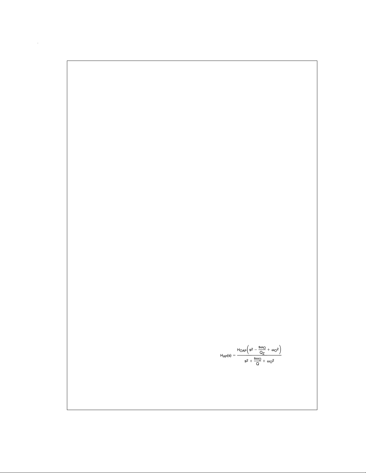
: the quality factor of the second order complex zero pair,
Q
Z
if any. Q
−
written:
,
where Q
H
OBP
H
OLP
(
Figure 2
H
OHP
(
Figure 3
is measured at the bandpass outputs of the
O
)
: the frequency of minimum (ideally zero) gain at the
is different from fOand if QZis high, it can be
z
)
Figure 6
.
is related to the allpass characteristic, which is
Z
=
Q for an all-pass response.
Z
: the gain (in V/V) of the bandpass output at f=fO.
: the gain (in V/V) of the lowpass output as f→0Hz
).
: the gain (in V/V) of the highpass output as f→f
).
divided by
O
Figure
CLK
/2
www.national.com 6
Page 7
1.0 Definition of Terms (Continued)
H
: the gain (in V/V) of the notch output as f→0 Hz and as
ON
f→f
/2, when the notch filter has equal gain above and
CLK
below the center frequency (
low-frequency gain differs from the high-frequency gain, as
in modes 2 and 3a (
Figure 11
ties below are used in place of H
and
Figure 4
Figure 8
.
ON
). When the
), the two quanti-
H
: the gain (in V/V) of the notch output as f→0 Hz.
ON1
: the gain (in V/V) of the notch output as f→f
H
ON2
CLK
/2.
(a)
(a)
DS010399-5
DS010399-7
(a)
DS010399-6
(b)
FIGURE 1. 2nd-Order Bandpass Response
DS010399-8
(b)
FIGURE 2. 2nd-Order Low-Pass Response
DS010399-9
DS010399-56
DS010399-57
DS010399-10
(b)
DS010399-58
FIGURE 3. 2nd-Order High-Pass Response
www.national.com7
Page 8

1.0 Definition of Terms (Continued)
(a)
(a)
(a) Bandpass
DS010399-11
DS010399-13
DS010399-12
(b)
FIGURE 4. 2nd-Order Notch Response
DS010399-14
(b)
FIGURE 5. 2nd-Order All-Pass Response
(b) Low Pass
DS010399-60
DS010399-61
(c) High-Pass
DS010399-50
(d) Notch
DS010399-53
FIGURE 6. Response of various 2nd-order filters as a function of Q.
Gains and center frequencies are normalized to unity.
www.national.com 8
DS010399-51
DS010399-52
(e) All-Pass
DS010399-54
Page 9

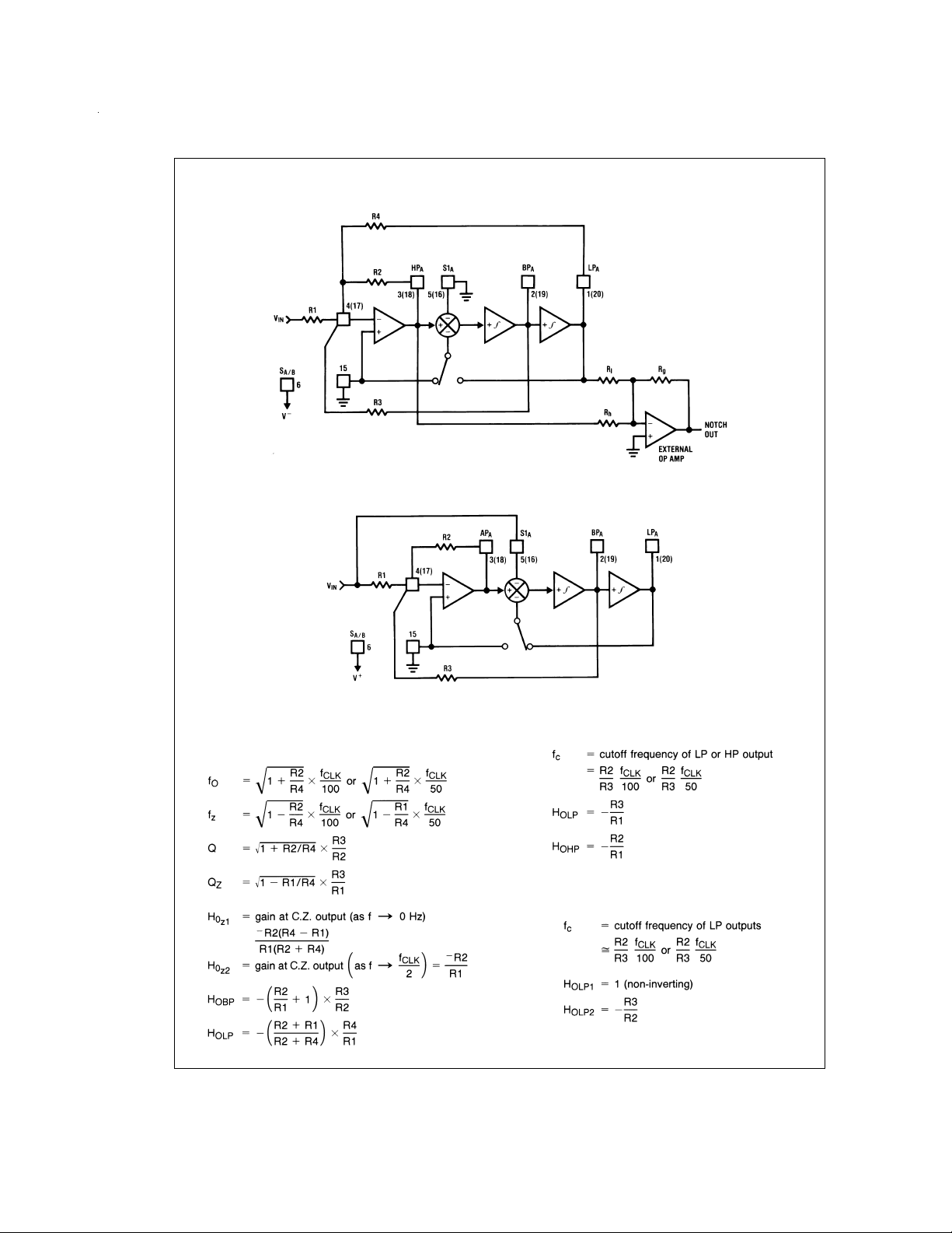
2.0 Modes of Operation
The MF10 is a switched capacitor (sampled data) filter. To
fully describe its transfer functions, a time domain approach
is appropriate. Since this is cumbersome, and since the
MF10 closely approximates continuous filters, the following
discussion is based on the well known frequency domain.
Each MF10 can produce a full 2nd order function. See
1
for a summary of the characteristics of the various modes.
MODE 1: Notch 1, Bandpass, Lowpass Outputs:
=
(See
Figure 7
f
f
notch
=
f
center frequency of the complex pole pair
O
O
)
Table
=
quality factor of the complex pole pair
BW=the −3 dB bandwidth of the bandpass output.
Circuit dynamics:
=
f
center frequency of the imaginary zero pair=f
notch
MODE 1a: Non-Inverting BP, LP (See
.
O
Note: VINshould be driven from a low impedance (<1kΩ) source.
FIGURE 7. MODE 1
DS010399-16
Figure 8
)
FIGURE 8. MODE 1a
DS010399-17
www.national.com9
Page 10

2.0 Modes of Operation (Continued)
MODE 2: Notch 2, Bandpass, Lowpass: f
(See
Figure 9
)
notch
<
MODE 3: Highpass, Bandpass, Lowpass Outputs
(See
Figure 10
f
O
)
FIGURE 9. MODE 2
www.national.com 10
DS010399-18
Page 11

2.0 Modes of Operation (Continued)
*
In Mode 3, the feedback loop is closed around the input summing amplifier; the finite GBW product of this op amp causes a slight Q enhancement. If this is a
problem, connect a small capacitor (10 pF − 100 pF) across R4 to provide some phase lead.
DS010399-19
FIGURE 10. MODE 3
MODE 3a: HP, BP, LP and Notch with External Op Amp
Figure 11
(See
)
MODE 4: Allpass, Bandpass, Lowpass Outputs
(See
Figure 12
*
Due to the sampled data nature of the filter, a slight mismatch of fzand f
occurs causing a 0.4 dB peaking around fOof the allpass filter amplitude
response (which theoretically should be a straight line). If this is
unacceptable, Mode 5 is recommended.
)
O
www.national.com11
Page 12
2.0 Modes of Operation (Continued)
DS010399-20
FIGURE 11. MODE 3a
FIGURE 12. MODE 4
MODE 5: Numerator Complex Zeros, BP, LP
Figure 13
(See
www.national.com 12
)
DS010399-21
MODE 6a: Single Pole, HP, LP Filter (See
Figure 14
MODE 6b: Single Pole LP Filter (Inverting and
Non-Inverting) (See
Figure 15
)
)
Page 13

2.0 Modes of Operation (Continued)
DS010399-22
FIGURE 13. MODE 5
DS010399-23
FIGURE 14. MODE 6a
TABLE 1. Summary of Modes. Realizable filter types (e.g. low-pass) denoted by asterisks.
Unless otherwise noted, gains of various filter outputs are inverting and adjustable by resistor ratios.
Mode BP LP HP N AP
1
***
(2) May need input buffer.
1a H
2
=
−Q H
OBP1
=
H
+1 high Q.
OBP2
+ 1 2 No Poor dynamics for
OLP
***
***
3
FIGURE 15. MODE 6b
Number
of
Resistors f
3No
3 Yes (above f
4 Yes Universal State-Variable
DS010399-24
Adjustable
CLK/fO
or f
/100)
CLK
CLK
Notes
/50
Filter. Best general-purpose
mode.
www.national.com13
Page 14
2.0 Modes of Operation (Continued)
Unless otherwise noted, gains of various filter outputs are inverting and adjustable by resistor ratios. (Continued)
Mode BP LP HP N AP
3a
4
5
6a
6b
TABLE 1. Summary of Modes. Realizable filter types (e.g. low-pass) denoted by asterisks.
Number
Adjustable
of
Resistors f
****
7 Yes As above, but also includes
CLK/fO
resistor-tuneable notch.
** *
** *
3 No Gives Allpass response with
=
H
OAP
4 Gives flatter allpass response
than above if R
**
3 Single pole.
2 Single pole.
Notes
−1 and H
1
3.0 Applications Information
The MF10 is a general-purpose dual second-order state
variable filter whose center frequency is proportional to the
frequency of the square wave applied to the clock input
(f
). By connecting pin 12 to the appropriate DC voltage,
CLK
the filter center frequency f
f
/100 or f
CLK
±
6%) by using a crystal clock oscillator, or can be easily var-
/50. fOcan be very accurately set (within
CLK
can be made equal to either
O
ied over a wide frequency range by adjusting the clock frequency.Ifdesired, the f
resistors as in
Figures 9, 10, 11, 13, 14, 15
ratio can be altered by external
CLK/fO
. The filter Q and
gain are determined by external resistors.
All of the five second-order filter types can be built using ei-
ther section of the MF10. These are illustrated in
through
Figure 5
related equations.
along with their transfer functions and some
Figure 6
shows the effect of Q on the
Figure 1
shapes of these curves. When filter orders greater than two
are desired, two or more MF10 sections can be cascaded.
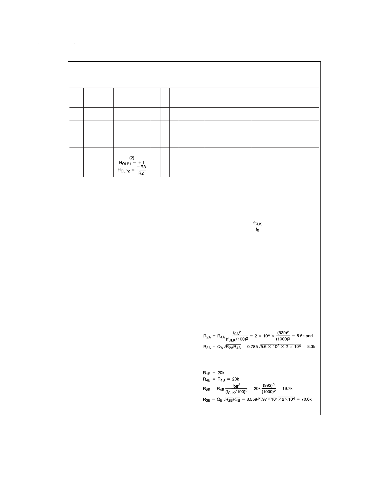
3.1 DESIGN EXAMPLE
In order to design a second-order filter section using the
MF10, we must define the necessary values of three parameters: f
, the filter section’s center frequency; H0, the pass-
0
band gain; and the filter’s Q. These are determined by the
characteristics required of the filter being designed.
As an example, let’s assume that a system requires a
fourth-order Chebyshev low-pass filter with 1 dB ripple, unity
gain at DC, and 1000 Hz cutoff frequency. As the system order is four, it is realizable using both second-order sections
of an MF10. Many filter design texts include tables that list
the characteristics (f
ter sections needed to synthesize a given higher-order filter.
and Q) of each of the second-order fil-
O
For the Chebyshev filter defined above, such a table yields
the following characteristics:
f
0A
f
0B
=
529 Hz Q
=
993 Hz Q
=
0.785
A
=
3.559
B
For unity gain at DC, we also specify:
=
1
H
0A
=
1
H
0B
The desired clock-to-cutoff-frequency ratio for the overall filter of this example is 100 and a 100 kHz clock signal is avail-
able. Note that the required center frequencies for the two
second-order sections will not be obtainable with
clock-to-center-frequency ratios of 50 or 100. It will be necessary to adjust
externally.From
Table1
, we see that Mode 3 can be used to
produce a low-pass filter with resistor-adjustable center frequency.
In most filter designs involving multiple second-order stages,
it is best to place the stages with lower Q values ahead of
stages with higher Q, especially when the higher Q is greater
than 0.707. This is due to the higher relative gain at the center frequency of a higher-Q stage. Placing a stage with lower
Q ahead of a higher-Q stage will provide some attenuation at
the center frequency and thus help avoid clipping of signals
near this frequency. For this example, stage A has the lower
Q (0.785) so it will be placed ahead of the other stage.
For the first section, we begin the design by choosing a convenient value for the input resistance: R
lute value of the passband gain H
choosing R
the 50/100/CL pin is connected to mid-supply for nominal
such that: R
4A
=
−H
4A
=
20k. The abso-
1A
is made equal to 1 by
OLPA
OLPAR1A
=
100:1 clock-to-center-frequency ratio, we find R
The resistors for the second section are found in a similar
fashion:
=
−2.
OLP
=
=
=
by:
0.02R
20k. If
.
4
R
2
R
1A
2A
www.national.com 14
Page 15

3.0 Applications Information
(Continued)
The complete circuit is shown in
power supplies. Supply bypass capacitors are highly
recommended.
FIGURE 16. Fourth-Order Chebyshev Low-Pass Filter from Example in 3.1.
Figure 16
±
5V Power Supply. 0V–5V TTL or −5V±5V CMOS Logic Levels.
for split±5V
DS010399-25
DS010399-26
FIGURE 17. Fourth-Order Chebyshev Low-Pass Filter from Example in 3.1.
Single +10V Power Supply. 0V–5V TTL Logic Levels. Input Signals
Should be Referred to Half-Supply or Applied through a Coupling Capacitor.
www.national.com15
Page 16
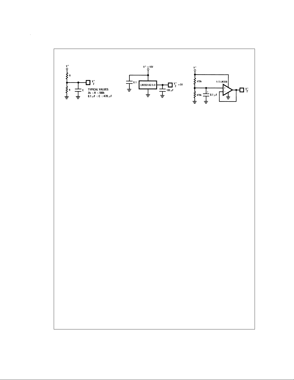
3.0 Applications Information (Continued)
DS010399-27
(a) Resistive Divider with
(b) Voltage Regulator
Decoupling Capacitor
FIGURE 18. Three Ways of Generating V
3.2 SINGLE SUPPLY OPERATION
The MF10 can also operate with a single-ended power sup-
Figure 17
ply.
power supply. V
tive power supply (8V to 14V), and V
nected to ground. The A
single supply operation. This half-supply point should be
shows the example filter with a single-ended
+
+
and V
A
are again connected to the posi-
D
GND
−
−
and V
D
are con-
A
pin must be tied to V+/2 for
very “clean”, as any noise appearing on it will be treated as
an input to the filter. It can be derived from the supply voltage
with a pair of resistors and a bypass capacitor (
Figure 18a
or a low-impedance half-supply voltage can be made using a
three-terminal voltage regulator or an operational amplifier
(
Figure 18b
and
Figure 18c
). The passive resistor divider
with a bypass capacitor is sufficient for many applications,
provided that the time constant is long enough to reject any
power supply noise. It is also important that the half-supply
reference present a low impedance to the clock frequency,
so at very low clock frequencies the regulator or op-amp approaches may be preferable because they will require
smaller capacitors to filter the clock frequency. The main
power supply voltage should be clean (preferably regulated)
and bypassed with 0.1 µF.
3.3 DYNAMIC CONSIDERATIONS
The maximum signal handling capability of the MF10, like
that of any active filter, is limited by the power supply voltages used. The amplifiers in the MF10 are able to swing to
within about 1V of the supplies, so the input signals must be
kept small enough that none of the outputs will exceed these
limits. If the MF10 is operating on
puts will clip at about 8 V
multiplied by the filter gain should therefore be less than
8V
.
p–p
±
5V,for example, the out-
. The maximum input voltage
p–p
Note that if the filter Q is high, the gain at the lowpass or
highpass outputs will be much greater than the nominal filter
gain (
Figure 6
10 will have a 20 dB peak in its amplitude response at f
the nominal gain of the filter H
will be 10. The maximum input signal at fOmust therefore be
less than 800 mV
supplies.
). As an example, a lowpass filter withaQof
is equal to 1, the gain at f
OLP
when the circuit is operated on±5V
p–p
O
Also note that one output can have a reasonable small voltage on it while another is saturated. This is most likely for a
circuit such as the notch in Mode 1 (
put will be very small at f
a large signal to the input. However, the bandpass will have
its maximum gain at f
put clips, the performance at the other outputs will be de-
O
and can clip if overdriven. If one out-
O
Figure 7
). The notch out-
, so it might appear safe to apply
graded, so avoid overdriving any filter section, even ones
.If
DS010399-28
(c) Operational Amplifier
with Divider
+
/2 for Single-Supply Operation
whose outputs are not being directly used. Accompanying
Figure 7
through
Figure 15
are equations labeled “circuit dynamics”, which relate the Q and the gains at the various outputs. These should be consulted to determine peak circuit
gains and maximum allowable signals for a given application.
3.4 OFFSET VOLTAGE
The MF10’s switched capacitor integrators have a higher
equivalent input offset voltage than would be found in a typi-
),
cal continuous-time active filter integrator.
an equivalent circuit of the MF10 from which the output DC
offsets can be calculated. Typical values for these offsets
with S
V
V
V
When S
DC offset at the BP output is equal to the input offset of the
lowpass integrator (V
depend on the mode of operation and the resistor ratios, as
=
os1
=
os2
=
os3
tied to V+are:
A/B
opamp offset
−150 mV
−70 mV
is tied to V−,V
A/B
=
±
5mV
@
50:1: −300 mV@100:1
@
50:1: −140 mV@100:1
will approximately halve. The
os2
). The offsets at the other outputs
os3
described in the following expressions.
O
Figure 19
DS010399-29
shows
www.national.com 16
Page 17

3.0 Applications Information
(Continued)
FIGURE 19. MF10 Offset Voltage Sources
DS010399-31
FIGURE 20. Method for Trimming V
OS
DS010399-30
www.national.com17
Page 18

3.0 Applications Information
(Continued)
For most applications, the outputs are AC coupled and DC
offsets are not bothersome unless large signals are applied
to the filter input. However, larger offset voltages will cause
clipping to occur at lower AC signal levels, and clipping at
any of the outputs will cause gain nonlinearities and will
change f
come excessively large if R2 and R4 are used to make
f
CLK/fO
if Q is also high. An extreme example is a bandpass filter
having unity gain,aQof20,andf
tied to ground (100:1 nominal). R4/R2 will therefore be equal
to 6.25 and the offset voltage at the lowpass output will be
about +1V. Where necessary, the offset voltage can be adjusted by using the circuit of
ment of V
outputs as described in the above equations. Some outputs
cannot be adjusted this way in some modes, however
(V
3.5 SAMPLED DATA SYSTEM CONSIDERATIONS
The MF10 is a sampled data filter, and as such, differs in
many ways from conventional continuous-time filters. An important characteristic of sampled-data systems is their effect
on signals at frequencies greater than one-half the sampling
frequency. (The MF10’s sampling frequency is the same as
its clock frequency.) If a signal with a frequency greater than
one-half the sampling frequency is applied to the input of a
sampled data system, it will be “reflected” to a frequency less
than one-half the sampling frequency. Thus, an input signal
whose frequency is f
and Q. When operating in Mode 3, offsets can be-
O
significantly higher than the nominal value, especially
=
250 with pin 12
CLK/fO
Figure 20
, which will have varying effects on the different
OS1
in modes 1a and 3, for example).
OS(BP)
/2 + 100 Hz will cause the system to re-
s
. This allows adjust-
spond as though the input frequency was f
phenomenon is known as “aliasing”, and can be reduced or
/2 − 100 Hz. This
s
eliminated by limiting the input signal spectrum to less than
f
/2. This may in some cases require the use of a
s
bandwidth-limiting filter ahead of the MF10 to limit the input
spectrum. However, since the clock frequency is much
higher than the center frequency,this will often not be necessary.
Another characteristic of sampled-data circuits is that the
output signal changes amplitude once every sampling period, resulting in “steps” in the output voltage which occur at
the clock rate (
Figure 21
). If necessary, these can be
“smoothed” with a simple R–C low-pass filter at the MF10
output.
The ratio of f
affect performance. A ratio of 100:1 will reduce any aliasing
to fC(normally either 50:1 or 100:1) will also
CLK
problems and is usually recommended for wideband input
signals. In noise sensitive applications, however, a ratio of
50:1 may be better as it will result in 3 dB lower output noise.
The 50:1 ratio also results in lower DC offset voltages, as
discussed in Section 3.4.
The accuracy of the f
of Q. This is illustrated in the curves under the heading “Typi-
ratio is dependent on the value
CLK/fO
cal Performance Characteristics”. As Q is changed, the true
value of the ratio changes as well. Unless the Q is low, the
error in f
cific application, use a mode that allows adjustment of the ra-
will be small. If the error is too large for a spe-
CLK/fO
tio with external resistors.
It should also be noted that the product of Q and f
limited to 300 kHz when f
5 kHz.
<
5 kHz, and to 200 kHz for f
O
should be
O
O
>
FIGURE 21. The Sampled-Data Output Waveform
www.national.com 18
DS010399-32
Page 19

Connection Diagram
Surface Mount and
Dual-In-Line Package
DS010399-4
Top View
Order Number MF10CCWM
See NS Package Number M20B
Order Number MF10ACN or MF10CCN
See NS Package Number N20A
www.national.com19
Page 20

Physical Dimensions inches (millimeters) unless otherwise noted
Molded Package (Small Outline) (M)
Order Number MF10ACWM or MF10CCWM
NS Package Number M20B
20-Lead Molded Dual-In-Line Package (N)
Order Number MF10ACN or MF10CCN
NS Package Number N20A
www.national.com 20
Page 21

Notes
MF10 Universal Monolithic Dual Switched Capacitor Filter
LIFE SUPPORT POLICY
NATIONAL’S PRODUCTS ARE NOT AUTHORIZED FOR USE AS CRITICAL COMPONENTS IN LIFE SUPPORT
DEVICES OR SYSTEMS WITHOUT THE EXPRESS WRITTEN APPROVAL OF THE PRESIDENT AND GENERAL
COUNSEL OF NATIONAL SEMICONDUCTOR CORPORATION. As used herein:
1. Life support devices or systems are devices or
systems which, (a) are intended for surgical implant
into the body, or (b) support or sustain life, and
whose failure to perform when properly used in
accordance with instructions for use provided in the
2. A critical component is any component of a life
support device or system whose failure to perform
can be reasonably expected to cause the failure of
the life support device or system, or to affect its
safety or effectiveness.
labeling, can be reasonably expected to result in a
significant injury to the user.
National Semiconductor
Corporation
Americas
Tel: 1-800-272-9959
Fax: 1-800-737-7018
Email: support@nsc.com
www.national.com
National does not assume any responsibility for use of any circuitry described, no circuit patent licenses are implied and National reserves the right at any time without notice to change said circuitry and specifications.
National Semiconductor
Europe
Fax: +49 (0) 1 80-530 85 86
Email: europe.support@nsc.com
Deutsch Tel: +49 (0) 1 80-530 85 85
English Tel: +49 (0) 1 80-532 78 32
Français Tel: +49 (0) 1 80-532 93 58
Italiano Tel: +49 (0) 1 80-534 16 80
National Semiconductor
Asia Pacific Customer
Response Group
Tel: 65-2544466
Fax: 65-2504466
Email: sea.support@nsc.com
National Semiconductor
Japan Ltd.
Tel: 81-3-5639-7560
Fax: 81-3-5639-7507
 Loading...