NSC LMX5080MX, LMX5080M Datasheet

LMX5080 PLLatinum 2.7 GHz Low Power Dual Modulus Prescaler for RF Personal
Communications
LMX5080
PLLatinum
™
2.7 GHz Low Power Dual Modulus
Prescaler for RF Personal Communications
General Description
The LMX5080 integrated dual modulus prescaler, is designed to be used in a synthesized local oscillator for
2.5 GHz wireless transceivers. It is fabricated using National’s 0.5µABiCV silicon BiCMOS process. The LMX5080 contains three dual modulus prescalers. Either a 128/130,
256/158 or a 512/514 prescaler can be selected for up to
2.7 Gz RF input frequencies. The prescaler inputs can be
driven either differentially, or single ended with the use of a
coupling capacitor on one of the inputs to ground. The
LMX5080 CMOS output is optimized to generate very stable,
low switching noise output signals. The LMX5080 prescaler
can be used in conjunction with a low frequency Phase Lock
Loop to form a frequency synthesizer suitable for UHF transceivers. Supply voltage can range from 2.7V to 5.5V. The
LMX5080 features low current consumption; typically 7.0 mA
at 5V V
CC
The LMX5080 is available in a 8-pin Small Outline (SOP)
surface mount plastic package.
Functional Block Diagram
Features
n 2.7V to 5.5V operation
n Low current consumption: 7 mA (typ)
n −40˚C to +85˚C low noise CMOS output
n Selectable dual modulus prescaler
128/130
256/258
512/514
n 8-pin small package outline (SOP)
Applications
n 2.5 GHz wireless communications systems (ISM)
n Direct Broadcast Satellite systems (DBS)
n Cable TV tuners (CATV)
PRELIMINARY
April 1999
@
5V
DS100940-1
PLLatinum™is a trademark of National Semiconductor Corporation.
© 1999 National Semiconductor Corporation DS100940 www.national.com

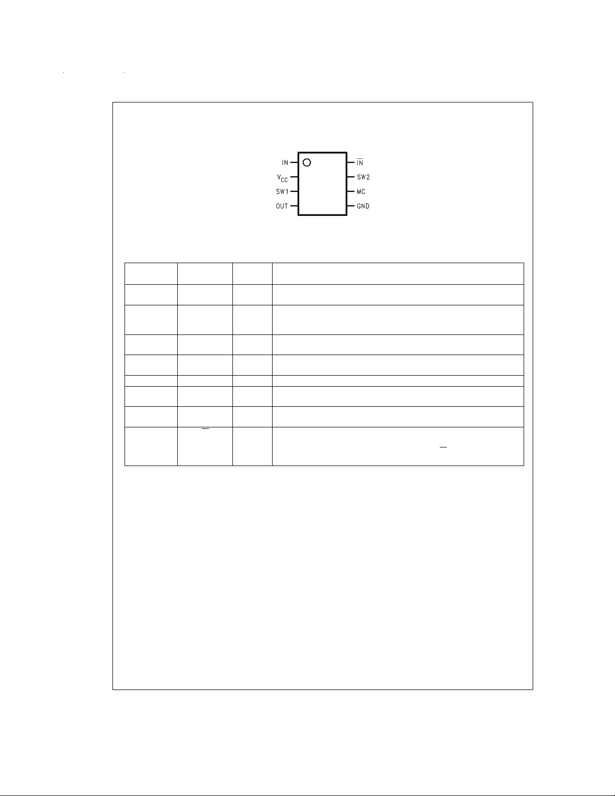
Connection Diagram
Small Outline Package (SOP)
DS100940-2
NS Package Number M08A
Order Number LMX5080M, LMX5080MX
Pin Descriptions
Pin
No.
1 IN I RF small signal prescaler input. Small signal input from the voltage controlled
2V
3 SW1 I Divide Ratio Control. CMOS logic input. Pin functionality is described in the
4 OUT O Prescaler Output. CMOS level output for connection to low frequency PLL
5 GND — Ground for analog and digital signals.
6 MC I Modulus Control Input. High impedance CMOS logic input. Pin functionality is
7 SW2 I Divide Ratio Control. High impedance CMOS logic input. Pin functionality is
8IN
Pin
Name
CC
I/O Description
oscillator
— Power Supply voltage input may range from 2.7V to 5.5V. Bypass capacitors
should be placed as close as possible to this pin and be connected directly
to the ground plane.
Modulus Control Truth Table.
input.
described in the Modulus Control Truth Table.
described in the Modulus Control Truth Table.
I RF small signal prescaler complementary input. In single-ended mode, a
bypass capacitor should be placed as close as possible to this pin and be
connected directly to the ground plane. The IN and IN can be driven
differentially when the bypass capacitor is omitted.
www.national.com 2

Absolute Maximum Ratings (Note 1)
If Military/Aerospace specified devices are required,
please contact the National Semiconductor Sales Office/
Recommended Operating
Conditions
Distributors for availability and specifications.
Parameter Symbol
Power Supply
Voltage V
Operating
Temperature T
Note 1: “Absolute Maximum Ratings” indicate limits beyond which damage
to the device may occur. Recommended Operating Conditions indicate conditions for which the deviceisintendedtobe functional, but do not guarantee
specific performance limits. Electrical Characteristics document specific minimum and/or maximum performance values at specified test conditions and
are guaranteed. Typ or Typical values are for informational purposes only
which are based on design parameters or device characterization and are not
guaranteed.
Note 2: This device is a high performance RF integrated circuit and is ESD
sensitive. Handling and assembly of this device should only be done on ESDfree workstations.
Parameter Symbol
Power Supply
Voltage V
Voltage on any
pin with
GND=0V V
Storage
Temperature
Range T
Lead Temp.
(solder 4 sec) T
Value
−0.3 6.5 V
CC
−0.3 VCC+0.3 V
i
−65 +1.50 ˚C
S
L
UnitsMin Typ Max
+2.60 ˚C
Electrical Characteristics
(VCC= 5.0V, T
Symbol Parameter Condition
I
CC
V
OH
V
OL
f
in
Pf
in
f
out
V
IH
V
IL
I
IH
I
IL
t
Set
IM Input/Output Intermodulation (Note 4) −10 dBm / 50Ω AC coupled
Note 3: See Timing Diagram.
Note 4: Guaranteed by design and characterization, not tested. Output frequency measured at input.
=
−40˚C to +85˚C except as specified) (Note 1)
A
Power Supply Current 7mA
Output Amplitude Z
Input Frequency AC coupled. V
Operational Input Signal Amplitude V
=
100 kΩ//10 pF
L
=
2.7V to 5.5V
V
CC
=
2.7V to 5.5V 100 2700 MHz
=
CC
CC
2.7V to 5.5V −15 +4 dBm
Output Frequency 0.1 25 MHz
High-level Input Voltage (MC, SW1,
SW2)
Low-level Input Voltage (MC, SW1,
SW2)
High-level Input Current (MC, SW1,
SW2)
Low-level Input Current (MC, SW1,
SW2)
=
V
0.7xV
IH
=
V
IL
0.3xV
CC
CC
Modulus Control Set-up time. (Note 3) SW1=H, SW2=H
=
2.7 GHz
f
in
signal delivered to input.
=
2.7V to 5.5V.
V
CC
MC=0, MC=1.
Fin=2.3 GHz to 2.5 GHz.
(Note 1)
2.7 5.5 V
CC
−40 +85 ˚C
A
Value
Min Typ Max
0.9xV
CC
0.7xV
CC
±
±
15 20 ns
−35 −30 dBc
Value
UnitsMin Typ Max
Units
V
0.1xV
V
CC
V
0.3xV
V
CC
1uA
1uA
www.national.com3
 Loading...