NSC LMX5001VBCX Datasheet

LMX5001
Dedicated Bluetooth Link Controller
General Description
The LMX5001 Dedicated Bluetooth™Link Controller has
been designed to interface with the LMX3162, Single Chip
Radio Transceiver to provide a rapid design path to a complete Bluetooth physical layer.
The LMX5001 also offers a low power and cost competitive
solution to the Bluetooth Link Controller function.
The LMX5001 can be attached to a Link Management Controller, or Host processor performing the Link Management
function to implement a complete Bluetooth interface.
Bluetooth is a world-wide recognized wireless communication standard, whichoperates in the ISM band (2.4 GHz), offering a low cost and convenient wireless replacement for
data/voice cable links between fixed and mobile electronic
devices.
Utilizing a GFSK modulation scheme, with frequency hopping, Bluetooth is able to offer a low power, low cost, robust
and spectrally efficient spread spectrum packet data system.
Features
n Bluetooth Specification 1.0B compliant
n Bluetooth physical layer, available today
n Supports Class 1, 2 and 3 Bluetooth (20 dBm, 4 dBm
and 0 dBm links)
n 1/8 bit sampling resolution
n Power management for Tx, Rx and PLL
n Piconet and Scatternet communication capable
n Good Bluetooth radio range coverage (when coupled
with the LMX3162)
n Support for RSSI channel quality monitoring
n Bluetooth Encryption Engine
Applications
n PCMCIA Cards
n Mobile Phones
n Laptop PCs
n Palmtop PCs
n Desktop PCs
n Computer Peripherals
n Wireless Modems
n PDAs
n Palmtops
n P.O.T.S
n Digital Cameras
n Fax
n Printers
n Bar-code Readers
n Notepads
n Cordless Headsets
n In-vehicle Communications
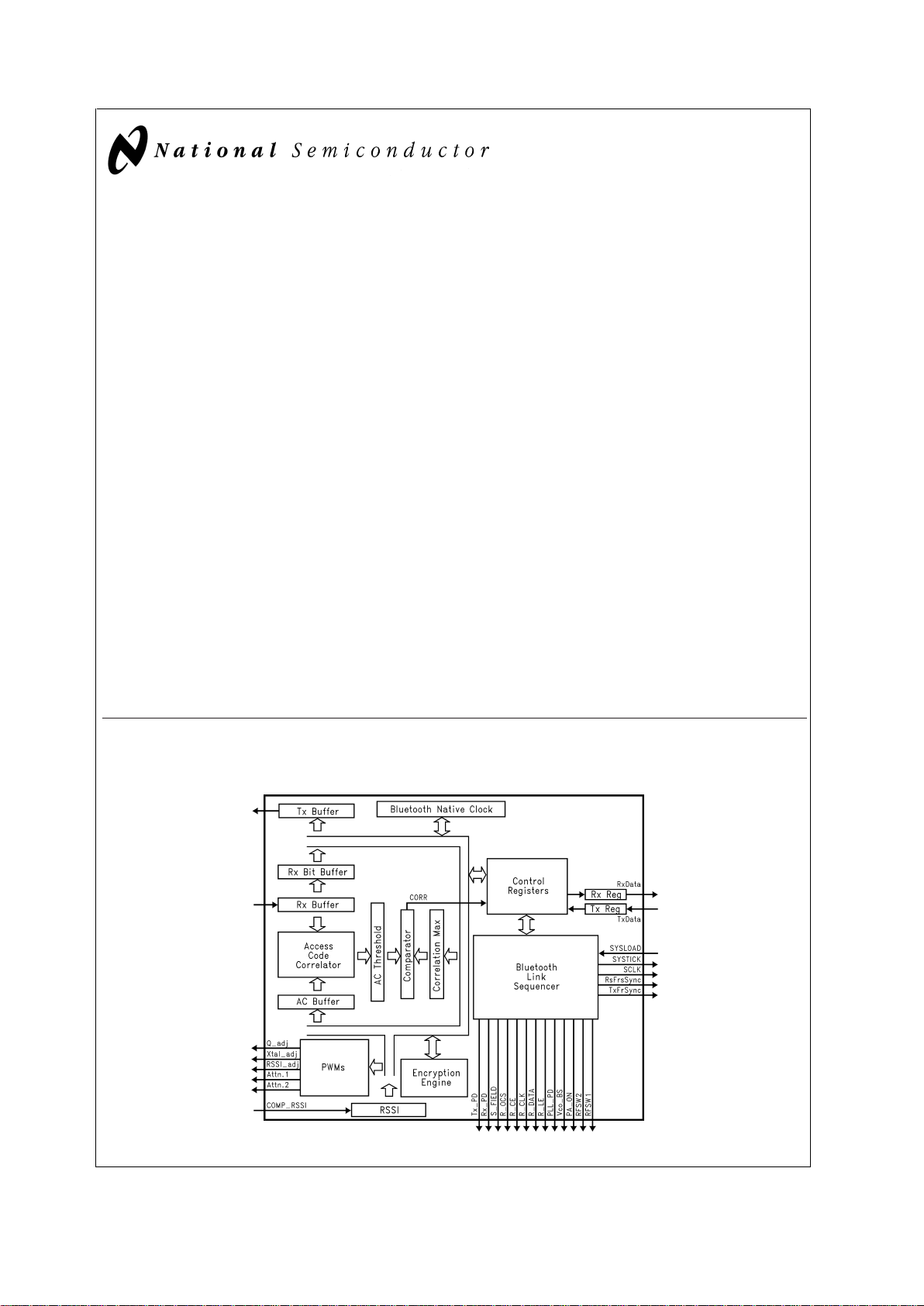
Block Diagram
Functional Block Diagram
DS101340-1
PRELIMINARY
April 2000
LMX5001 Dedicated Bluetooth Link Controller
© 2000 National Semiconductor Corporation DS101340 www.national.com

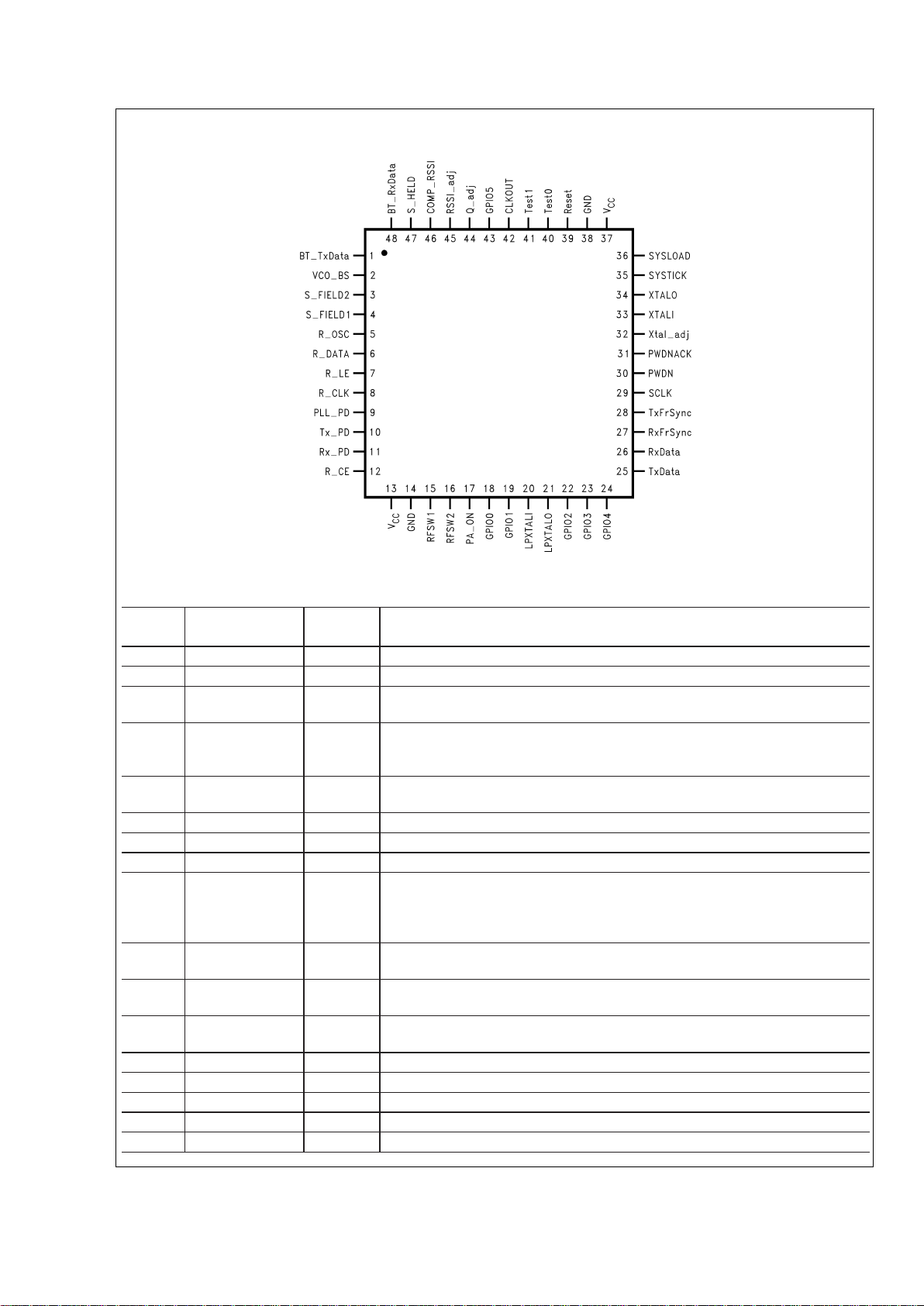
Connection Diagram
Pin Descriptions
Pin
No.
Pin Name I/O Description
1 BT_TxData O Transmit data
2 VCO_BS O VCO band switch control signal.
3 S_FIELD2 O LMX3162 DC compensation circuit enable. This signal is enabled (low) throughout
the correlation phase.
4 S_FIELD1 O LMX3162 DC compensation circuit enable. At the beginning of the correlation
phase this signal is enabled (low) for 15 µs. For the remainder of the correlation
phase this signal is PWM by 1/8 (cycle time = 1 µs).
5 R_OSC O LMX3162 4 MHz oscillator input to the PLL synthesizer. This signal is only
enabled when the LMX3162 is active.
6 R_DATA O MICROWIRE
™
data to LMX3162.
7 R_LE O MICROWIRE load enable to LMX3162.
8 R_CLK O MICROWIRE clock to LMX3162.
9 PLL_PD O LMX3162 PLL power down. This signal is used to open the PLL loop or powering
down the PLL. The PLL loop is opened when transmitting to make it possible to
FSK modulate the VCO. When receiving it is optional to open the PLL loop
(configured by the PLLOpenRX bit in threshold_msb).
10 Tx_PD O LMX3162 Transmitter power down. For power conservation, the Transmitter is
only powered during Transmit Frames.
11 Rx_PD O LMX3162 Receiver power down. For power conservation, the Receiver is only
powered during Receive Frames.
12 R_CE O LMX3162 chip enable. When the LMX5001 is in Idle Mode the LMX3162 is
powered down.
13 V
CC
Power +3.3V
14 GND Power 0V
15 RFSW1 O Antenna switch control.
16 RFSW2 O Antenna switch control. This signal is RFSW1 inverted,
17 PA_ON O Switches the external PA on/off for 20 dBm/0 dBm transmission, respectively.
DS101340-7
LMX5001
www.national.com 2

Pin Descriptions (Continued)
Pin
No.
Pin Name I/O Description
18 GPIO0
(XTAL Config)
I/O XTAL configuration during reset (Note 1).
19 GPIO1
(XTAL Config)
I/O XTAL configuration during reset (Note 1).
20 LPXTALI I 128 kHz XTAL connection for low power mode. This is used in low power mode. If
the low power mode is not used it is not necessary with at XTAL here. External
128 kHz clock can also be feed in here.
21 LPXTALO O 128 kHz XTAL connection.
22 GPIO2 I/O General Purpose I/O
23 GPIO3 I/O General Purpose I/O
24 GPIO4 I/O General Purpose I/O
25 TxData I LCI Data Transmit
26 RxData O LCI Data Receive
27 RxFrSync O LCI Receive Frame Sync.
28 TrFrSync O LCI Transmit Frame Sync.
29 SCLK O LCI Serial Clock.
30 PWDN O Power Down to Link Management Controller
31 PWDNACK I Power Down Acknowledge from Link Management Controller
32 Xtal_adj O PWM signal to make adjustments to the XTAL.
33 XTALI I 16 MHz XTAL connection. (External clock input).
34 XTALO O 16 MHz XTAL connection.
35 SYSTICK O Systick generated from the internal LMX5001 Master/Slave Counter.
36 SYSLOAD I When low holds the LMX5001 in Idle Mode. A rising edge causes a system load
After a rising edge the LMX5001 will start to load control data from and store
status information to the LMC via the LCI.
37 V
CC
Power
38 GND Power
39 Reset I Reset. After Reset is released the LMX5001 will be in Idle Mode, awaiting a
SYSLOAD.
40 Test0 I Should be tied low. This signal is used in production test.
41 Test1 I Should be lied low. This signal is used in production test.
42 CLKOUT O Xtal clock output to Link Management Controller. This signal can be disabled
using the Sysload Command (for power saving).
43 GPIO5 I/O General Purpose I/O
44 Q_adj O PWM signal to make it possible to adjust the quadrature tank circuit to the
LMX3162.
45 RSSI_adj O PWM signal for use in creating an RSSI AD converter.
46 COMP_RSSI I Output from the external comparator in the RSSI AD converter.
47 S_Field3 O DC Compensation circuit enable. At the beginning of the correlation phase, this
signal is enabled (low) for 15 µs.
48 BT_RxData I Receive data.
Note 1: During Reset GPIO0 and GPIO1aresampledto setup the Xtal division ratio. The assumed external Xtal frequency is derived using the following relationship:
GPIO1 GPIO0 Xtal Division Ratio
Low Low Divide by 2 (i.e., 16 MHz XTAL or clock input).
Low High Divide by 3 (i.e., 24 MHz XTAL or clock input).
High Low Divide by 4 (i.e., 32 MHz XTAL or clock input).
High High Not used.
After Reset is completed, GPIO0 and GPIO1 can be used as normal general purpose I/Os.
LMX5001
www.national.com3

Absolute Maximum Ratings (Note 2)
If Military/Aerospace specified devices are required,
please contact the National Semiconductor Sales Office/
Distributors for availability and specifications.
Operating Ambient Temperature 0˚C to +70˚C
Storage Temperature −65˚C to +150˚C
Maximum Input Voltage:
Inputs V
DD
+0.5V
5V Tolerant V
DD5
+0.5V
Maximum Operating Voltage 3.6V
Note 2: Stresses beyond those listed under “Absolute Maximum Ratings”
may cause permanent damage to the device. This is a stress rating only and
functional operation of the device at these or any other conditions beyond
those indicated in the operational sections of this specification is not implied.
Exposure to absolute maximum rating conditions for extended periods may
affect device reliability.
DC Electrical Characteristics
Symbol Parameter Conditions Min Typ Max Units
T
A
Ambient Temperature 0 70 ˚C
V
DD
Supply Voltage 3.0 3.3 3.6 V
I
IH
High-Level Input Current VIN=VDD;VDD=V
DDmax
10 µA
I
IL
Low-Level Input Current VIN=VSS;VDD=V
DDmax
, −10 µA
I
OZ
High-Impedance State Output
Current
VIN=VDDor VSS,VDD=V
DDmax
,
−10 10
µA
I
OC
Output Short-Circuit Current
This is true for all outputs
except crystal outputs XTALO
and LPXTALO.
V
OUT=VDD;VDD=VDDmax
70
mA
V
OUT=VSS;VDD=VDDmax
−45
V
IH
High-Level Input Voltage 2.0 1.7 V
V
IL
Low-Level Input Voltage 1.1 0.8 V
V
OH
High-Level Output Voltage IOH= As rated; VDD=V
DDmin
all outputs except XTALO and
LPXTALO are rated with IOH = 10ma
and IOL = -10mA. XTALO is rated
+/-8mA and LPXTALO is rated +/-2mA.
0.7 V
DD
V
V
OL
Low-Level Output Voltage IOL= As rated; VDD=V
DDmin
all outputs except XTALO and
LPXTALO are rated with IOH = 10ma
and IOL = -10mA. XTALO is rated
+/-8mA and LPXTALO is rated +/-2mA.
0.4 V
Functional Description
BLUETOOTH COMMUNICATION
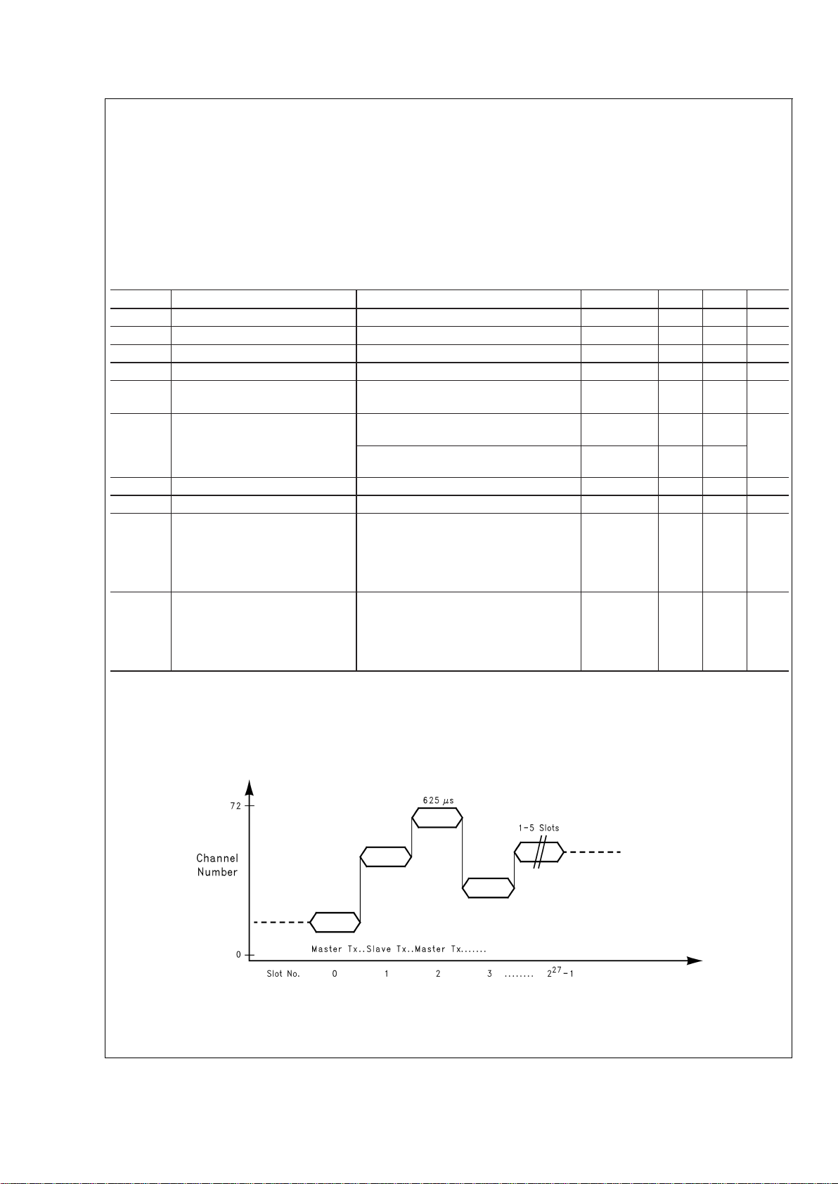
The following illustrates a Bluetooth, Frequency Hopping, TDD, Packet based communication link:
The LMX5001 performs all the necessary functions and interconnect to permit the LMX3162 to be operated as a Blue-
DS101340-2
FIGURE 1. Bluetooth Frequency Hopping TDD
LMX5001
www.national.com 4
 Loading...