

NSC LMX3161VBHX, LMX3161VBH Datasheet
LMX3161
Single Chip Radio Transceiver
General Description
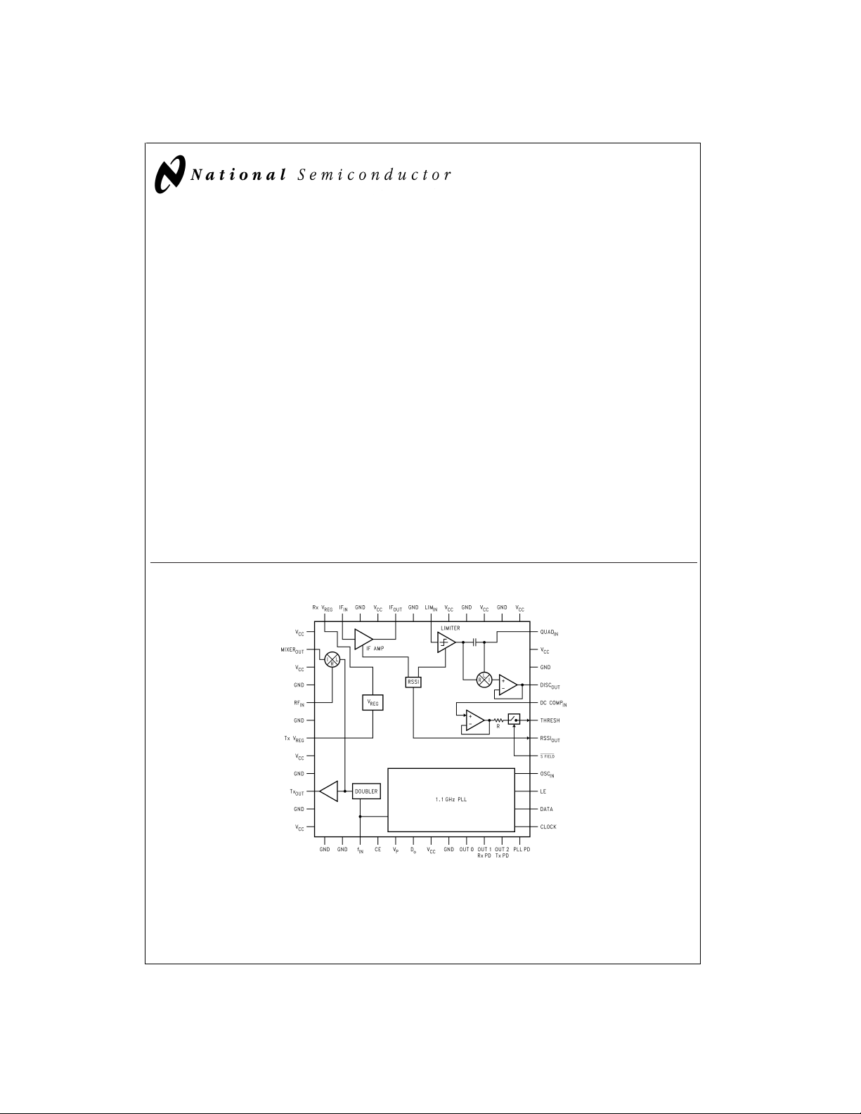
The LMX3161 Single Chip Radio Transceiverisamonolithic,
integrated radio transceiver optimized for use in a Digital Enhanced Cordless Telecommunications (DECT) system. It is
fabricated using National’s ABiC V BiCMOS process
=
(f
18 GHz).
T
The LMX3161 contains phase locked loop (PLL), transmit
and receive functions. The 1.1 GHz PLL block is shared between transmit and receive section. The transmitter includes
a frequency doubler, and a high frequency buffer. The receiver consists of a 2.0 GHz lownoisemixer,anintermediate
frequency (IF) amplifier, a high gain limiting amplifier, a frequency discriminator, a received signal strength indicator
(RSSI), and an analog DC compensation loop. The PLL,
doubler, and buffers can be used to implement open loop
modulation along with an external VCO and loop filter. The
circuit features on-chip voltage regulation to allow supply
voltages ranging from 3.0V to 5.5V. Two additional voltage
regulators provide a stable supply source to external discrete stages in the Tx and Rx chains.
The IF amplifier, high gain limiting amplifier, and discriminator are optimized for 110 MHz operation, with a total IF gain
of 85 dB. The single conversion receiver architecture pro-
LMX3161 Single Chip Radio Transceiver
PRELIMINARY
November 1999
vides a low cost, high performance solution for communications systems. The RSSI output may be used for channel
quality monitoring.
The Single Chip Radio Transceiver is available in a 48-pin
7mm X 7mm X 1.4mm PQFP surface mount plastic package.
Features
n Single chip solution for DECT RF transceiver
n RF sensitivity to −93 dBm; RSSI sensitivity to −100 dBm
n Two regulated voltage outputs for discrete amplifiers
n High gain (85 dB) intermediate frequency strip
n Allows unregulated 3.0V–5.5V supply voltage
n Power down mode for increased current savings
n System noise figure 6.5 dB (typ)
Applications
n Digital Enhanced Cordless Telecommunications (DECT)
n Personal wireless communications (PCS/PCN)
n Wireless local area networks (WLANs)
n Other wireless communications systems
Block Diagram
DS012815-1
MICROWIRE™is a trademark of National Semiconductor Corporation.
®
TRI-STATE
is a registered trademark of National Semiconductor Corporation.
© 1999 National Semiconductor Corporation DS012815 www.national.com
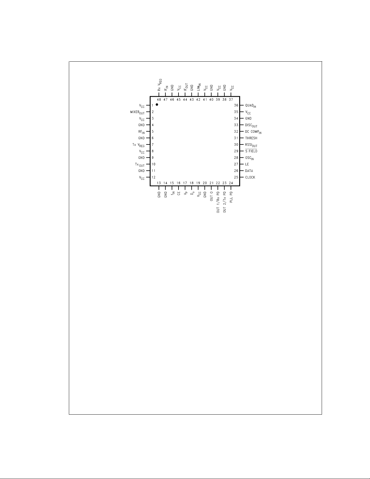
LMX3161 Pin Diagram
LMX3161
DS012815-2
Top View
Order Number LMX3161VBH or LMX3161VBHX
See NS Package Number VBH48A
www.national.com 2
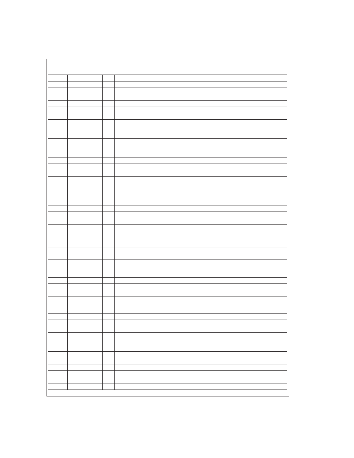
LMX3161 Pin Diagram (Continued)
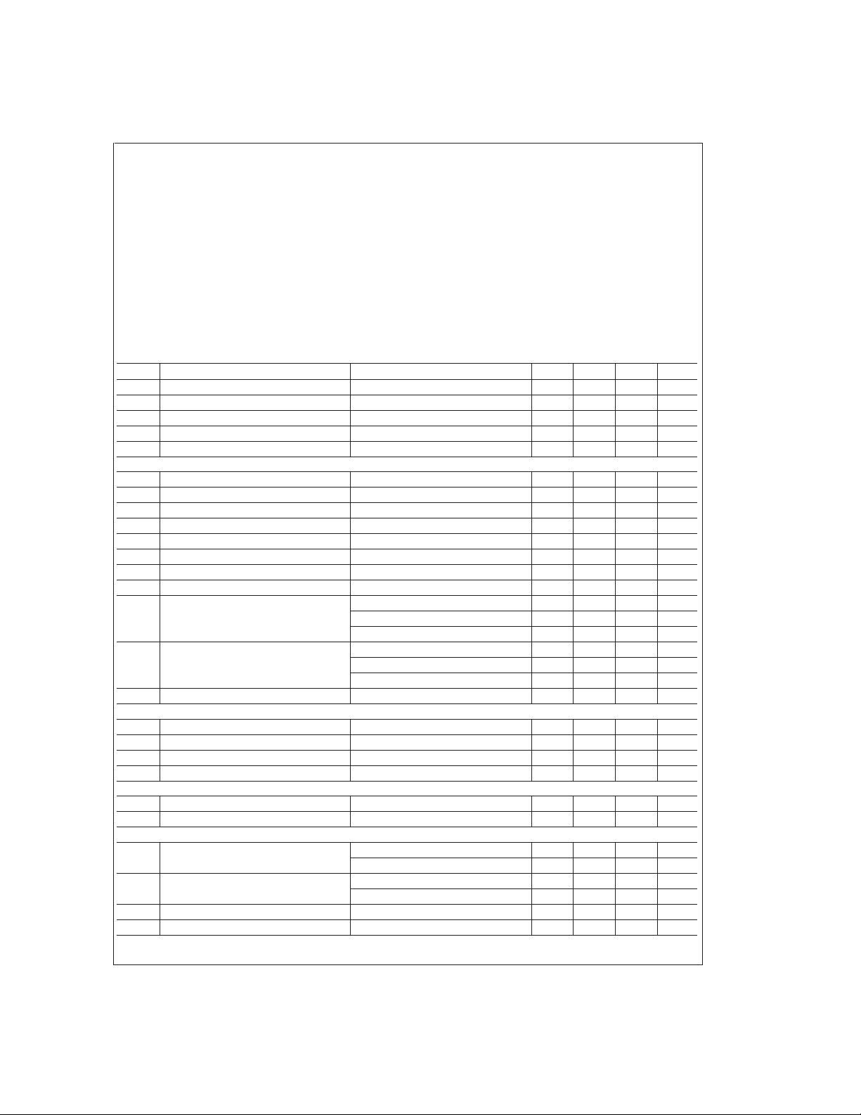
Pin No. Pin Name I/O Description
1V
2 MIXER
3V
CC
OUT
CC
4 GND — Ground.
5RF
IN
6 GND — Ground.
7TxV
8V
REG
CC
9 GND — Ground.
10 Tx
OUT
11 GND — Ground.
12 V
CC
13 GND — Ground.
14 GND — Ground.
15 f
IN
16 CE I Chip Enable. Pulling LOW powers down entire chip. Taking CE HIGH powers up the
17 V
18 D
19 V
P
o
CC
20 GND — Ground.
21 OUT 0 O Programmable CMOS output. Refer to Function Register Programming Description section
22 Rx PD/OUT 1 I/O Receiver power down control input or programmable CMOS output. Refer to Function
23 Tx PD/OUT 2 I/O Transmitter power down control input or programmable CMOS output. Refer to Function
24 PLL PD I PLL power down control input. LOW for PLL normal operations, and HIGH for PLL power
25 CLOCK I MICROWIRE
26 DATA I MICROWIRE data input. High impedance CMOS input with Schmitt Trigger.
27 LE I MICROWIRE load enable input. High impedance CMOS input with Schmitt Trigger.
28 OSC
IN
29 S FIELD
30 RSSI
OUT
31 THRESH O Threshold level to external comparator.
32 DC COMP
33 DISC
OUT
34 GND — Ground.
35 V
CC
36 QUAD
37 V
CC
38 GND — Ground.
39 V
CC
40 GND — Ground.
41 V
CC
— Power supply for CMOS section of PLL and ESD bussing.
O IF output from the mixer.
— Power supply for mixer section.
I RF input to the mixer.
— Regulated power supply for external PA gain stage.
— Power supply for analog sections of PLL and doubler.
O Frequency doubler output.
— Power supply for analog sections of PLL and doubler.
I RF Input to PLL and frequency doubler.
appropriate functional blocks depending on the state of bits F6, F7, F11, and F12
programmed in F-latch. It is necessary to initialize the internal registers once, after the
power up reset. The registers’ contents are kept even in power-down condition.
— Power supply for charge pump.
O Charge pump output. For connection to a loop filter for driving the input of an external VCO.
— Power supply for CMOS section of PLL and ESD bussing.
for details.
Register Programming Description section for details.
Register Programming Description section for details.
saving.
™
clock input. High impedance CMOS input with Schmitt Trigger.
I Oscillator input. High impedance CMOS input with feedback.
I DC compensation circuit enable. While LOW, the DC compensation circuit is enabled and
the threshold is updated through the DC compensation loop. While HIGH, the switch is
opened, and the comparator threshold is held by the external capacitor.
O Received signal strength indicator (RSSI) output.
I Input to DC compensation circuit.
IN
O Demodulated output of discriminator.
— Power supply for the discriminator circuit.
IN
I Quadrature input for tank circuit.
— Power supply for limiter output stage.
— Power supply for limiter gain stages.
— Power supply for IF amplifier gain stages.
LMX3161
www.national.com3
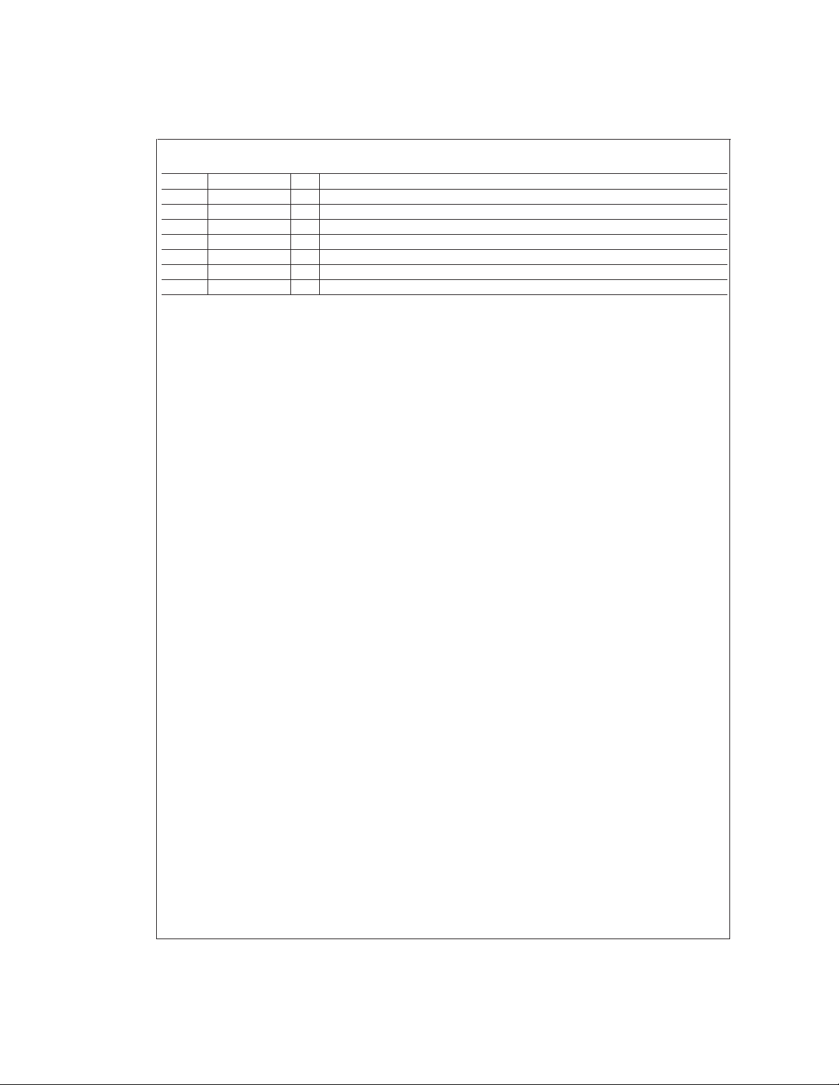
LMX3161 Pin Diagram (Continued)
Pin No. Pin Name I/O Description
LMX3161
42 LIM
IN
43 GND — Ground.
44 IF
45 V
OUT
CC
46 GND — Ground.
47 IF
48 Rx V
IN
REG
I IF input to the limiter.
O IF output from IF amplifier.
— Power supply for IF amplifier output.
I IF input to IF amplifier.
— Regulated power supply for external LNA stages.
www.national.com 4
Absolute Maximum Ratings (Notes 1, 2)
Power Supply Voltage (V
V
P
Voltage on Any Pin with
GND=0V (V
) −0.3V to VCC+0.3V
I
Storage Temperature Range (T
Lead Temp. (solder, 4 sec)(T
) −0.3V to +6.5V
CC
−0.3V to +6.5V
) −65˚C to +150˚C
S
) +260˚C
L
Recommended Operating
Conditions
Supply Voltage (VCC) 3.0V to 5.5V
Operating Temperature (T
Note 1: Absolute Maximum Ratings indicate limits beyond which damage to
the device may occur. Recommended Operating Conditions indicate conditions for which the device is intended to be functional, but do not guarantee
specific performance limits. For guaranteed specifications and test conditions, see the Electrical Characteristics section. The guaranteed specifications apply only for the test conditions listed.
Note 2: This device is a high performance RFintegrated circuit with an ESD
<
KeV and is ESD sensitive. Handling and assembly of this device
rating
should only be done at ESD work stations.
)V
(V
P
) −10˚C to +70˚C
A
CC
to 5.5V
Electrical Characteristics
The following specifications are guaranteed for V
CC
=
3.6V and T
Symbol Parameter Conditions Min Typ Max Unit
Current Consumption
I
DD, RX
I
DD, TX
I
DD, PLL
I
PD
MIXER f
f
RF
f
IF
Z
Z
-Open-Loop Receive Mode PLL & TX chain powered down — 50 60 mA
-Open-Loop Transmit Mode PLL & RX chain powered down — 27 37 mA
-Closed-Loop PLL Mode RX & TX chain powered down — 6 8 mA
-Power Down Mode — — 70 µA
=
RF
RF Frequency Range (Note 3) 1.7 — 2.0 GHz
IF Frequency (Note 4) — 110 — MHz
Input Impedance, RF
IN
Output Impedance, Mixer Out —
OUT
IN
NF Noise Figure (Single Side Band) (Notes 5, 6) — 10 14 dB
G
P
Conversion Gain (Note 5) 14 17 — dB
C
Input 1dB Compression Point (Note 5) −24 −20 — dBm
1dB
OIP3 Output 3rd Order Intercept Point (Note 5) — 7.5 — dBm
F
-RF Fin to RF Isolation F
IN
F
-IF Fin to IF Isolation f
IN
RF–IF RF to IF Isolation P
IF AMPLIFIER f
=
890 MHz — −30 — dB
IN
=
f
1780 MHz — −10.6 — dB
IN
=
f
2670 MHz — −30 — dB
IN
=
890 MHz — −30 — dB
IN
=
f
1780 MHz — −30 — dB
IN
=
f
2670 MHz — −30 — dB
IN
=
0 to −85 dB — −30 — dB
IN
=
110 MHz
IN
NF Noise Figure (Note 7) — 8 11 dB
A
Z
Z
IF LIMITER f
Gain (Note 7) 15 24 — dB
V
Input Impedance —
IN
Output Impedance —
OUT
IN
=
110 MHz
Sens Limiter/Discriminator Sensitivity BER=10
IF
DISCRIMINATOR f
IF Limiter Input Impedance —
IN
IN
=
110 MHz
Disc Gain 1X Mode — 10 — mV/˚
(mV/˚ of Phase Shift from Tank Circuit) 3X Mode — 33 — mV/˚
V
Discriminator Output Peak to Peak 1X Mode (Note 8) 80 160 — mV
OUT
Voltage 3X Mode (Note 8) 400 580 — mV
V
DISC
Disc. Output DC Voltage Nominal (Note 10) 1.2 1.82 V
OS
Disc. Output Impedance — 300 — Ω
OUT
A
1.89 GHz, f
−3
=
25˚C, unless otherwise specified.
=
IF
110 MHz, f
=
LO
1780 MHz (f
=
890 MHz)
IN
15-j5
—
160-j70
150–j120
190–j20
— Ω
— Ω
— Ω
— Ω
— −65 — dBm
100–j300
— Ω
LMX3161
www.national.com5
 Loading...