NSC LMV7219M7, LMV7219M5X, LMV7219M5, LMV7219M7X Datasheet

April 2000
LMV7219
7 nsec, 2.7V to 5V Comparator with Rail-to Rail Output
LMV7219 7 nsec, 2.7V to 5V Comparator with Rail-to Rail Output
General Description
The LMV7219 is a low-power, high-speed comparator with
internal hysteresis. The LMV7219 operating voltage ranges
from 2.7V to 5V with push/pull rail-to-rail output. This device
achieves a 7ns propagation delay while consuming only
1.1mA of supply current at 5V.
The LMV7219 inputs have a common mode voltage range
that extends 200mVbelow ground, allowing ground sensing.
The internal hysteresis ensures clean output transitions even
with slow-moving inputs signals.
The LMV7219 is available in the SC70-5 and SOT23-5 packages, which are ideal for systems where small size and low
power are critical.
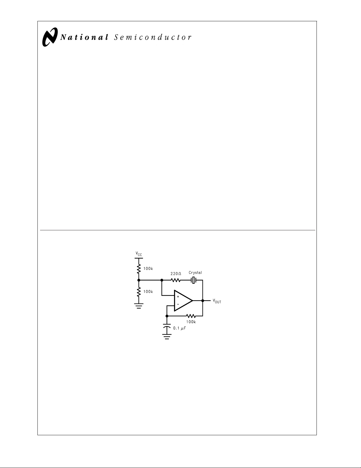
Typical Application
Features
(VS=5V,TA= 25˚C, Typical values unless specified)
n Propagation delay 7ns
n Low supply current 1.1mA
n Input common mode voltage range extends 200mv
below ground
n Ideal for 2.7V and 5V single supply applications
n Internal hysteresis ensures clean switching
n Fast rise and fall time 1.3ns
n Available in space-saving packages:
5-pin SC70-5
SOT23-5
Applications
n Portable and battery-powered systems
n Scanners
n Set top boxes
n High speed differential line receiver
n Window comparators
n Zero-crossing detectors
n High-speed sampling circuits
DS101054-1
© 2000 National Semiconductor Corporation DS101054 www.national.com

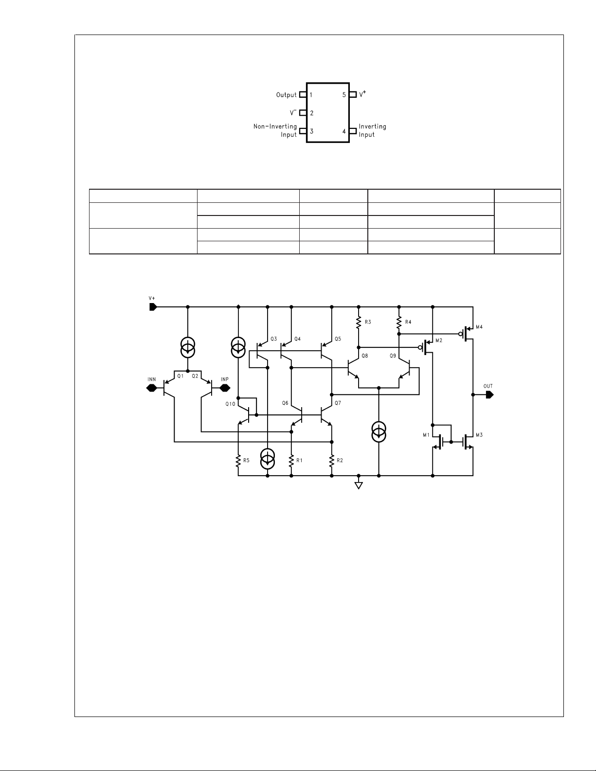
Connection Diagram
LMV7219
Ordering Information
Package Part Number Marking Supplied as NSC Drawing
5-pin SC70-5
5-pin SOT23-5
Simplified Schematic
SC70-5/SOT23-5
DS101054-2
Top View
LMV7219M7 C15 1k Units Tape and Reel
LMV7219M7X C15 3k Units Tape and Reel
LMV7219M5 C14A 1k Units Tape and Reel
LMV7219M5X C14A 3k Units Tape and Reel
MAA05A
MA05B
www.national.com 2
DS101054-3

LMV7219
Absolute Maximum Ratings (Note 1)
If Military/Aerospace specified devices are required,
Voltage at Input/Output pins
Current at Input Pin (Note 9)
please contact the National Semiconductor Sales Office/
Distributors for availability and specifications.
ESD Tolerance (Note 2)
Machine Body 150V
Human Model Body 2000V
Differential Input Voltage
±
Supply Voltage
Output Short Circuit Duration (Note 3)
Supply Voltage (V
+-V−
) 5.5V
Soldering Information
Operating Ratings
Supply voltages (V+-V−) 2.7V to 5V
Junction temperature range
(Note 4)
Storage Temperature Range −65˚C to +150˚C
Package Thermal Resistance
SC70-5 478˚C/W
SOT23-5 265˚C/W
−40˚C to +85˚C
Infrared or Convection (20 sec) 235˚C
Wave Soldering (10 sec) 260˚C (lead temp)
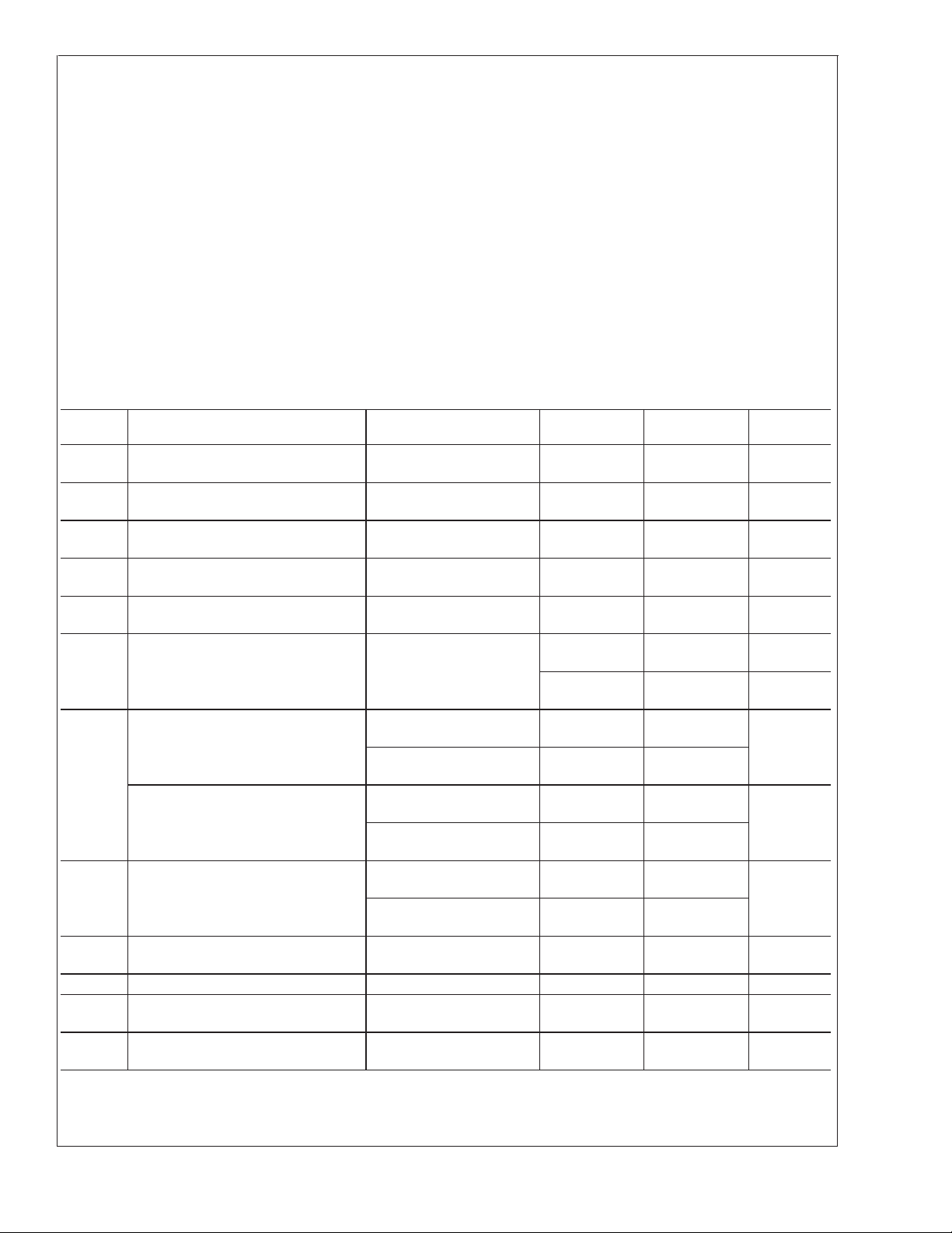
2.7V Electrical Characteristics
Unless otherwise specified, all limits guaranteed for TJ= 25˚C, VCM=V+/2, V+= 2.7V, V−= 0V, CL= 10pF and R
−
V
. Boldface limits apply at the temperature extremes.
Symbol Parameter Conditions Typ
(Note 5)
V
OS
I
B
I
OS
CMRR Common Mode Rejection Ratio 0V
PSRR Power Supply Rejection Ratio V
V
CM
Input Offset Voltage 1 6
Input Bias Current 450 950
Input Offset Current 50 200
<
<
V
1.50V 85 62
CM
+
= 2.7V to 5V 85 65
Input Common-Voltage Range CMRR>50dB VCC−1 VCC−1.2
−0.2 −0.1
V
I
I
V
V
V
SC
S
O
HYST
TRIP
TRIP
Output Swing High IL= 4mA,
= 500mV
V
ID
= 0.4mA,
I
L
= 500mV
V
ID
Output Swing Low I
= −4mA,
L
= −500mV
V
ID
= −0.4mA,
I
L
= −500mV
V
ID
Output Short Circuit Current Sourcing,
= 0V (Note 3)
V
O
Sinking,
V
= 2.7V (Note 3)
O
Supply Current No load 0.9 1.6
Input Hysteresis Voltage (Note 10) 7 mV
+
Input Referred Positive Trip Point (see
−
Input Referred Negative Trip Point (see
Figure 1
Figure 1
)38mV
)−4−8mV
V
CC
V
CC
130 200
15 50
20
20
−0.22 VCC−0.3
−0.02 VCC−0.05
Limit
(Note 6)
8
2000
400
55
55
V
CC
0
V
CC
−0.15
V
CC
300
150
2.2
−1.3
−0.4
L
>
1MΩ to
Units
mV
max
nA
max
nA
max
dB
min
dB
min
V
min
V
max
V
min
mV
max
mA
mA
max
max
min
www.national.com3

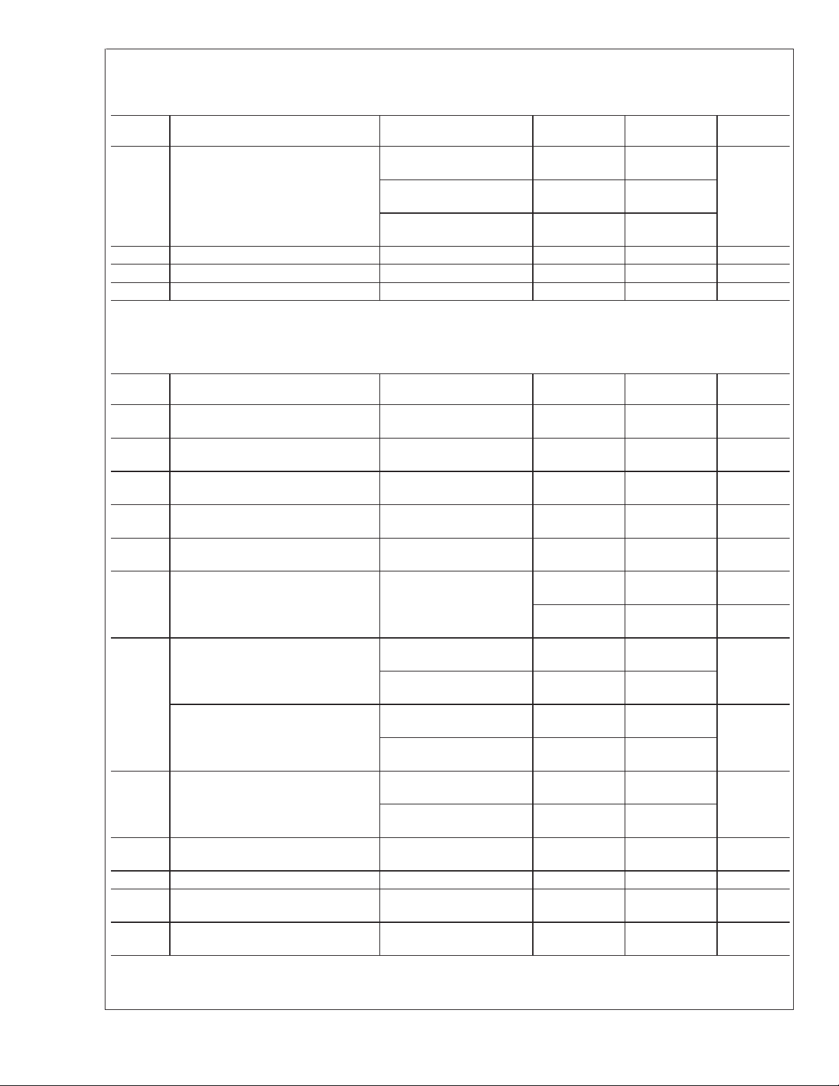
2.7V Electrical Characteristics (Continued)
Unless otherwise specified, all limits guaranteed for TJ= 25˚C, VCM=V+/2, V+= 2.7V, V−= 0V, CL= 10pF and R
LMV7219
V−. Boldface limits apply at the temperature extremes.
Symbol Parameter Conditions Typ
(Note 5)
t
PD
t
SKEW
t
r
t
f
Propagation Delay Overdrive = 5mV
= 0V (Note 7)
V
CM
Overdrive = 15mV
V
= 0V (Note 7)
CM
Overdrive = 50mV
V
= 0V (Note 7)
CM
Propagation Delay Skew (Note 8) 1 ns
Output Rise Time 10% to 90% 2.5 ns
Output Fall Time 90% to 10% 2 ns
12
11
10 20
5V Electrical Characteristics
Unless otherwise specified, all limits guaranteed for TJ= 25˚C, VCM=V+/2, V+= 5V, V−= 0V, CL= 10pF and R
V−. Boldface limits apply at the temperature extremes.
Symbol Parameter Conditions Typ
V
OS
I
B
I
OS
CMRR Common Mode Rejection Ratio 0V
PSRR Power Supply Rejection Ratio V
V
CM
V
O
I
SC
Input Offset Voltage 1 6
Input Bias Current 500 950
Input Offset Current 50 200
<
<
V
3.8V 85 65
CM
+
= 2.7V to 5V 85 65
Input Common-Mode Voltage Range CMRR>50dB VCC−1 VCC−1.2
Output Swing High IL= 4mA,
= 500mV
V
ID
= 0.4mA,
I
L
= 500mV
V
ID
Output Swing Low I
= −4mA,
L
= −500mV
V
ID
= −0.4mA,
I
L
= −500mV
V
ID
Output Short Circuit Current Sourcing, VO=0V
(Note 3)
Sinking, V
O
=5V
(Note 3)
I
V
V
V
S
HYST
Trip
Trip
Supply Current No load 1.1 1.8
Input Hysteresis Voltage (Note 10) 7.5 mV
+
Input Referred Positive Trip Point (See figure 1) 3.5 8 mV
−
Input Referred Negative Trip Point (See figure 1) −4 −8 mV
(Note 5)
−0.2 −0.1
V
−0.13 VCC−0.2
CC
V
−0.02 VCC−0.05
CC
80 180
10 50
68 30
65 30
V
Limit
(Note 6)
Limit
(Note 6)
8
2000
400
55
55
−1.3
V
CC
0
−0.3
V
CC
−0.15
CC
280
150
20
20
2.4
L
>
L
>
1MΩ to
1MΩ to
Units
ns
max
Units
mV
max
nA
max
nA
max
dB
min
dB
min
V
min
V
max
V
min
mV
max
mA
min
mA
max
max
min
www.national.com 4
 Loading...