

NSC LMV431BCMDC, LMV431BCM5X, LMV431AIMFX, LMV431AIMF, LMV431BCM5 Datasheet

LMV431/LMV431A/LMV431B
Low-Voltage (1.24V) Adjustable Precision Shunt
Regulators
General Description
The LMV431, LMV431A and LMV431B are precision 1.24V
shunt regulators capable of adjustment to 30V. Negative
feedback from the cathode to the adjust pin controls the
cathode voltage, much like a non-inverting op amp configuration (Refer to Symbol and Functional diagrams). A two
resistor voltage divider terminated at the adjust pin controls
the gain of a 1.24V band-gap reference. Shorting the cathode to the adjust pin (voltage follower) provides a cathode
voltage of a 1.24V.
The LMV431, LMV431A and LMV431B have respective initial tolerances of 1.5%, 1% and 0.5%, and functionally lends
themselves to several applications that require zener diode
type performance at low voltages. Applications include a 3V
to 2.7V low drop-out regulator, an error amplifier in a 3V
off-line switching regulator and even as a voltage detector.
These parts are typically stable with capacitive loads greater
than 10nF and less than 50pF.
The LMV431, LMV431A and LMV431B provide performance
at a competitive price.
Features
n Low Voltage Operation/Wide Adjust Range (1.24V/30V)
n 0.5% Initial Tolerance (LMV431B)
n Temperature Compensated for Industrial Temperature
Range (39 PPM/˚C for the LMV431AI)
n Low Operation Current (55µA)
n Low Output Impedance (0.25Ω)
n Fast Turn-On Response
n Low Cost
Applications
n Shunt Regulator
n Series Regulator
n Current Source or Sink
n Voltage Monitor
n Error Amplifier
n 3V Off-Line Switching Regulator
n Low Dropout N-Channel Series Regulator
Connection Diagrams
TO92: Plastic Package
10095801
Top View
SOT23-5
10095844
*
Pin 1 is not internally connected.
*
Pin 2 is internally connected to Anode pin. Pin 2 should be either floating
or connected to Anode pin.
Top View
SOT23-3
10095867
Top View
August 2003
LMV431/LMV431A/LMV431B Low-Voltage (1.24V) Adjustable Precision Shunt Regulators
© 2003 National Semiconductor Corporation DS100958 www.national.com
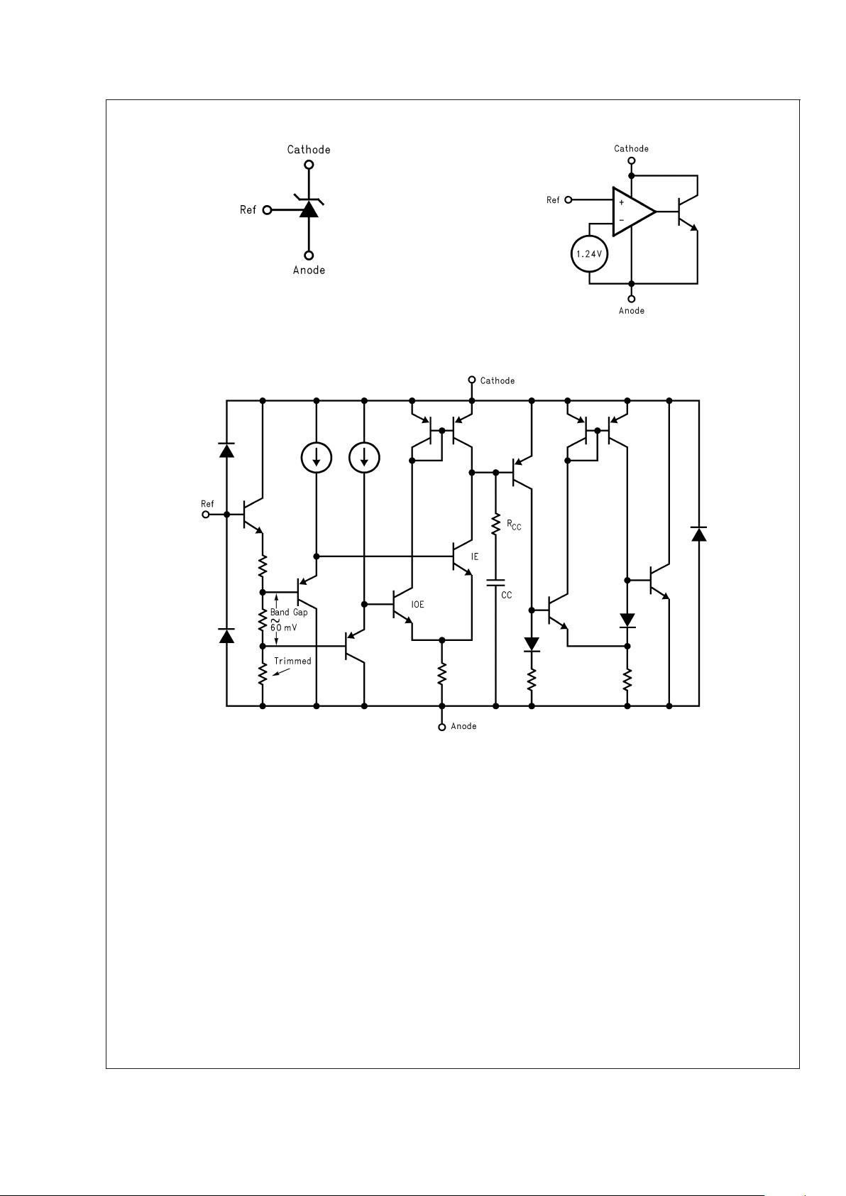
Symbol and Functional Diagrams
10095859
10095860
Simplified Schematic
10095803
LMV431/LMV431A/LMV431B
www.national.com 2
Ordering Information
Package Temperature
Range
Voltage Tolerance Part Number Package Marking NSC Drawing
TO92
Industrial Range
−40˚C to +85˚C
1% LMV431AIZ LMV431AIZ
Z03A
1.5% LMV431IZ LMV431IZ
Commerial Range
0˚C to +70˚C
0.5% LMV431BCZ LMV431BCZ
1% LMV431ACZ LMV431ACZ
1.5% LMV431CZ LMV431CZ
SOT23-5
Industrial Range
−40˚C to +85˚C
1% LMV431AIM5 N08A
MF05A
1% LMV431AIM5X N08A
1.5% LMV431IM5 N08B
1.5% LMV431IM5X N08B
Commercial Range
0˚C to +70˚C
0.5% LMV431BCM5 N09C
0.5% LMV431BCM5X N09C
1% LMV431ACM5 N09A
1% LMV431ACM5X N09A
1.5% LMV431CM5 N09B
1.5% LMV431CM5X N09B
SOT23-3
Industrial Range
−40˚ to +85˚C
0.5% LMV431BIMF
RLB
MF03A
0.5% LMV431BIMFX
1% LMV431AIMF
RLA
1% LMV431AIMFX
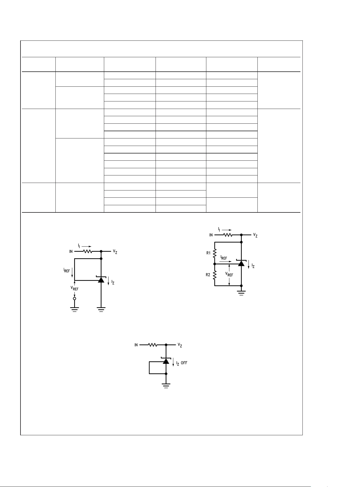
DC/AC Test Circuits for Table and
Curves
10095804
FIGURE 1. Test Circuit for VZ=V
REF
10095805
Note: VZ=V
REF
(1 + R1/R2) + I
REF
•
R1
FIGURE 2. Test Circuit for V
Z
>
V
REF
10095806
FIGURE 3. Test Circuit for Off-State Current
LMV431/LMV431A/LMV431B
www.national.com3
Absolute Maximum Ratings (Note 1)
If Military/Aerospace specified devices are required,
please contact the National Semiconductor Sales Office/
Distributors for availability and specifications.
Storage Temperature Range −65˚C to +150˚C
Operating Temperature Range
Industrial (LMV431AI, LMV431I) −40˚C to +85˚C
Commercial (LMV431AC,
LMV431C, LMV431BC)
0˚C to +70˚C
Lead Temperature
TO92 Package/SOT23 -5,-3 Package
(Soldering, 10 sec.) 265˚C
Internal Power Dissipation (Note 2)
TO92
0.78W
SOT23-5, -3 Package 0.28W
Cathode Voltage 35V
Continuous Cathode Current −30 mA to +30mA
Reference Input Current range −.05mA to 3mA
Operating Conditions
Cathode Voltage V
REF
to 30V
Cathode Current 0.1 mA to 15mA
Temperature range
LMV431AI −40˚C ≤ T
A
≤ 85˚C
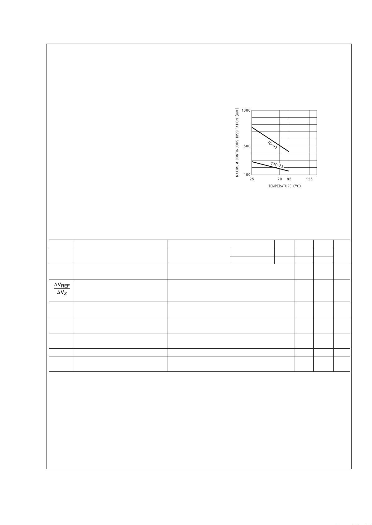
Thermal Resistance (θ
JA
)(Note 3)
SOT23-5, -3 Package 455 ˚C/W
TO-92 Package 161 ˚C/W
Derating Curve (Slope = −1/θ
JA
)
10095830
LMV431C Electrical Characteristics
TA= 25˚C unless otherwise specified
Symbol Parameter Conditions Min Typ Max Units
V
REF
Reference Voltage VZ=V
REF,IZ
= 10mA
(See Figure 1 )
TA= 25˚C 1.222 1.24 1.258
T
A
= Full Range 1.21 1.27 V
V
DEV
Deviation of Reference Input Voltage
Over Temperature (Note 4)
VZ=V
REF,IZ
= 10mA,
T
A
= Full Range (See Figure 1)
412mV
Ratio of the Change in Reference
Voltage to the Change in Cathode
Voltage
I
Z
= 10mA (see Figure 2 )
V
Z
from V
REF
to 6V
R
1
= 10k, R2=∞and 2.6k
−1.5 −2.7 mV/V
I
REF
Reference Input Current R1= 10kΩ,R2=
∞
II= 10mA (see Figure 2)
0.15 0.5 µA
∝
I
REF
Deviation of Reference Input Current
over Temperature
R1= 10kΩ,R2=∞,
I
I
= 10mA, TA= Full Range (see Figure 2)
0.05 0.3 µA
I
Z(MIN)
Minimum Cathode Current for
Regulation
VZ=V
REF
(see Figure 1)5580µA
I
Z(OFF)
Off-State Current VZ=6V, V
REF
=0V(see Figure 3 ) 0.001 0.1 µA
r
Z
Dynamic Output Impedance (Note 5) VZ=V
REF,IZ
= 0.1mA to 15mA
Frequency = 0Hz (see Figure 1) 0.25 0.4 Ω
LMV431/LMV431A/LMV431B
www.national.com 4
LMV431I Electrical Characteristics
TA= 25˚C unless otherwise specified
Symbol Parameter Conditions Min Typ Max Units
V
REF
Reference Voltage VZ=V
REF,IZ
= 10mA
(See Figure 1 )
TA= 25˚C 1.222 1.24 1.258
V
T
A
= Full Range 1.202 1.278
V
DEV
Deviation of Reference Input Voltage
Over Temperature (Note 4)
VZ=V
REF,IZ
= 10mA,
T
A
= Full Range (See Figure 1)
620mV
Ratio of the Change in Reference
Voltage to the Change in Cathode
Voltage
I
Z
= 10mA (see Figure 2 )
V
Z
from V
REF
to 6V
R
1
= 10k, R2=∞and 2.6k
−1.5 −2.7 mV/V
I
REF
Reference Input Current R1= 10kΩ,R2=
∞
II= 10mA (see Figure 2)
0.15 0.5 µA
∝
I
REF
Deviation of Reference Input Current
over Temperature
R1= 10kΩ,R2=∞,
I
I
= 10mA, TA= Full Range (see Figure 2)
0.1 0.4 µA
I
Z(MIN)
Minimum Cathode Current for
Regulation
VZ=V
REF
(see Figure 1)
55 80 µA
I
Z(OFF)
Off-State Current VZ= 6V, V
REF
=0V(see Figure 3 ) 0.001 0.1 µA
r
Z
Dynamic Output Impedance (Note 5) VZ=V
REF,IZ
= 0.1mA to 15mA
Frequency = 0Hz (see Figure 1) 0.25 0.4 Ω
LMV431AC Electrical Characteristics
TA= 25˚C unless otherwise specified
Symbol Parameter Conditions Min Typ Max Units
V
REF
Reference Voltage VZ=V
REF,IZ
=10mA
(See Figure 1 )
TA= 25˚C 1.228 1.24 1.252
V
T
A
= Full Range 1.221 1.259
V
DEV
Deviation of Reference Input Voltage
Over Temperature (Note 4)
VZ=V
REF,IZ
= 10mA,
T
A
= Full Range (See Figure 1)
412mV
Ratio of the Change in Reference
Voltage to the Change in Cathode
Voltage
I
Z
=10mA(see Figure 2 )
V
Z
from V
REF
to 6V
R
1
= 10k, R2=∞and 2.6k
−1.5 −2.7 mV/V
I
REF
Reference Input Current R1=1kΩ,R2=
∞
II=10mA(see Figure 2)
0.15 0.50 µA
∝
I
REF
Deviation of Reference Input Current
over Temperature
R1=10kΩ,R2=∞,
I
I
= 10 mA, TA= Full Range (see Figure 2)
0.05 0.3 µA
I
Z(MIN)
Minimum Cathode Current for
Regulation
VZ=V
REF
(see Figure 1)
55 80 µA
I
Z(OFF)
Off-State Current VZ= 6V, V
REF
=0V(see Figure 3 ) 0.001 0.1 µA
r
Z
Dynamic Output Impedance (Note 5) VZ=V
REF,IZ
= 0.1mA to 15mA
Frequency = 0 Hz (see Figure 1) 0.25 0.4 Ω
LMV431/LMV431A/LMV431B
www.national.com5
 Loading...