

NSC LMP8100MAX, LMP8100 Datasheet
July 2007
LMP8100
Programmable Gain Amplifier
General Description
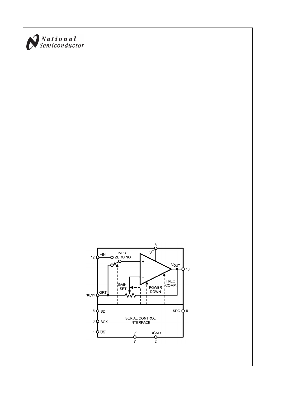
The LMP8100 programmable gain amplifier features an adjustable gain from 1 to 16 V/V in 1 V/V increments. At the core
of the LMP8100 is a precision, 33 MHz, CMOS input, rail-torail input/output operational amplifier with a typical open-loop
gain of 110 dB. Amplifier closed-loop gain is set by an array
of precision thin-film resistors. Amplifier control modes are
programmed via a serial port that allows devices to be cascaded so that an array of LMP8100 amplifiers can be programmed by a single serial data stream. The control mode
registers are double buffered to insure glitch-free transitions
between programmed settings. The LMP8100 is part of the
LMP® precision amplifier family and is ideal for a variety of
applications.
The amplifier features several programmable controls including: gain; a power-conserving shutdown mode which can
reduce current consumption to only 20 μA; an input zeroing
switch which allows the output offset voltage to be measured
to facilitate system calibration; and four levels of internal frequency compensation which can be set to maximize bandwidth at the different gain settings.
The LMP8100 comes in a 14-Pin SOIC package.
Features
Typical Values, TA = 25°C
■
Gain error (over temperature range)
—
LMP8100A 0.03%
—
LMP8100 0.075%
■
Gain range 1 to 16 V/V in 1 V/V steps
■
Programmable frequency compensation
■
Input zero calibration switch
■
Input offset voltage (max, LMP8100A)
250 μV
■
Input bias current 0.1 pA
■
Input noise voltage 12 nV/√Hz
■
Unity gain bandwidth 33 MHz
■
Slew rate 12 V/μs
■
Output current 20 mA
■
Supply voltage range 2.7V to 5.5V
■
Supply current 5.3 mA
■
Rail-to-Rail output swing V+ −50 mV to V− +50 mV
Applications
■
Industrial instrumentation
■
Data acquisition systems
■
Test equipment
■
Scaling amplifier
■
Gain control
■
Sensor interface
Simplified Block Diagram
20147607
LMP® is a registered trademark of National Semiconductor Corporation.
© 2007 National Semiconductor Corporation 201476 www.national.com
LMP8100 Programmable Gain Amplifier
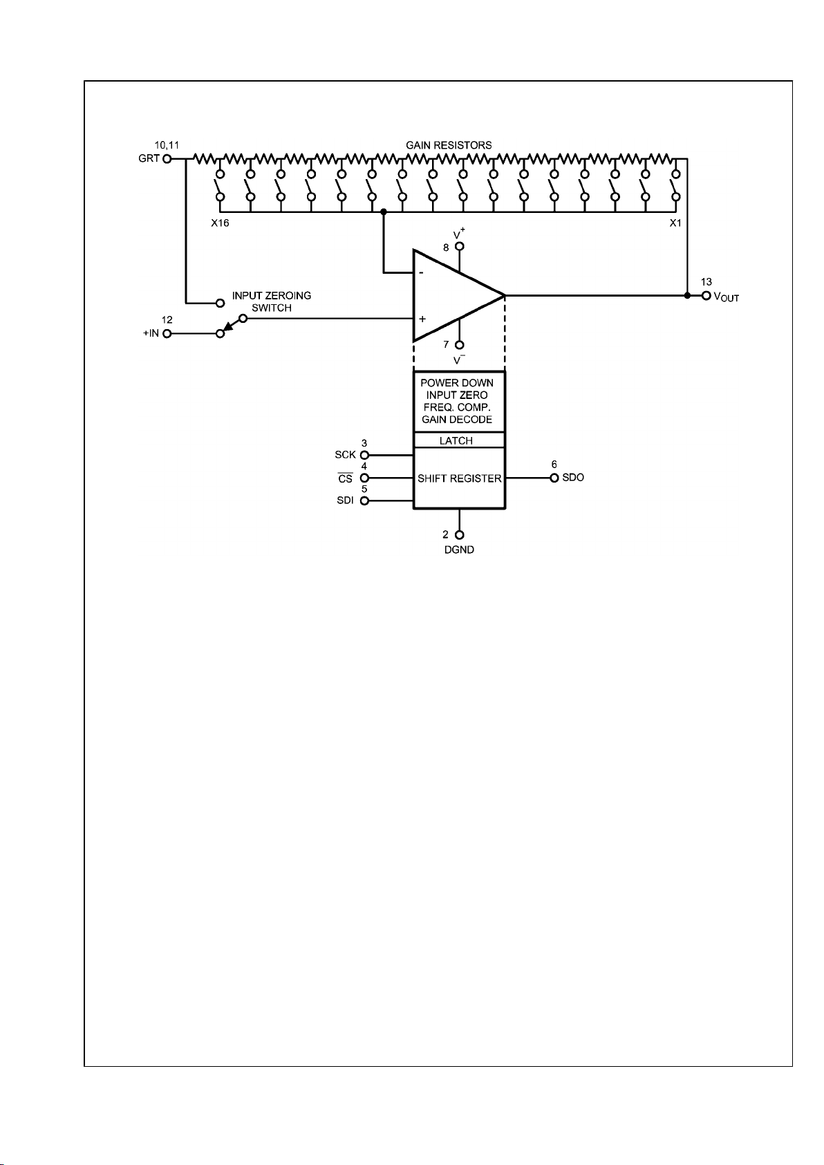
Block Diagram
20147602
www.national.com 2
LMP8100
Absolute Maximum Ratings (Note 1)
If Military/Aerospace specified devices are required,
please contact the National Semiconductor Sales Office/
Distributors for availability and specifications.
ESD Tolerance (Note 2)
Human Body Model 2 kV
Machine Model 200V
VIN Differential
2.5V
Output Short Circuit Duration (Note 3)
Supply Voltage (VS = V+ – V−)
6V
Voltage at Input and Output Pins V+ +0.3V, V− −0.3V
Input Current ±10 mA
Storage Temperature Range −65°C to +150°C
Junction Temperature (Note 4) +150°C
Soldering Information
Lead Temperature, Infrared or
Convection Reflow (20 sec) 235°C
Lead Temperature, Wave Solder (10
sec) 260°C
Operating Ratings (Note 1)
Supply Voltage (VS = V+ – V−)
2.7V to 5.5V
Junction Temperature Range (Note 4)
LMP8100A −40°C to +125°C
LMP8100 −40°C to +85°C
Package Thermal Resistance (θJA (Note 4)
14-Pin SOIC 145°C/W
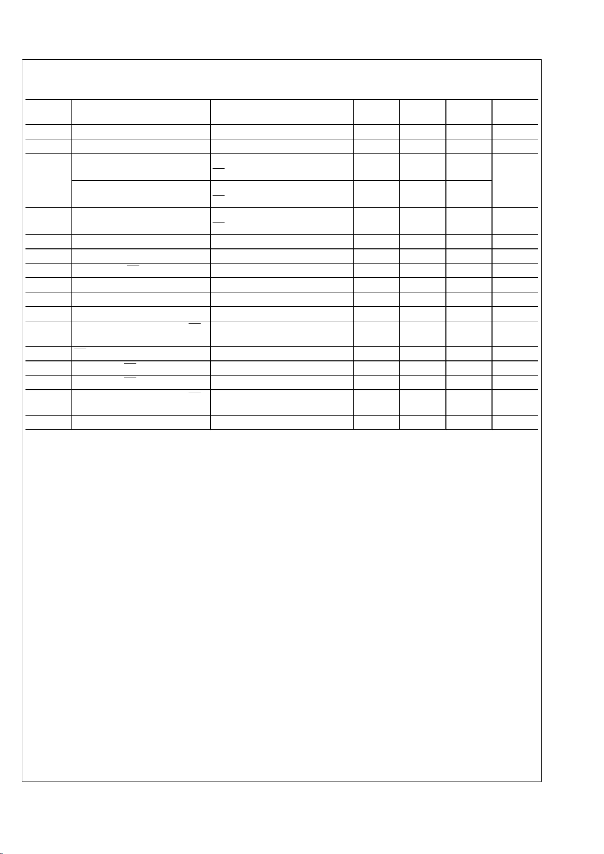
5V Electrical Characteristics
Unless otherwise specified, all limits are guaranteed for TA = 25°C. V+ = 5V , V– = 0V, DGND = 0V, +IN = GRT = V+/2, RL = 10
kΩ to V+/2; Gain = 1 V/V. Boldface limits apply at the temperature extremes.
Symbol Parameter Conditions Min
(Note 6)
Typ
(Note 5)
Max
(Note 6)
Units
Gain Error LMP8100A 0V < +IN (DC) < 3.5V,
1 V/V ≤ Gain ≤ 16 V/V,
0.5V < V
OUT
< 4.5V
0.015 0.03
0.03
%
Gain Error LMP8100 0.015 0.075
0.075
LMP8100 Gain Error (Gain = 1 V/V)
Extended +IN Range
+IN > 3.5V,
0.3V < V
OUT
< 4.7V
0.1
0.2
%
TCGE Gain Drift LMP8100A Gain = 16 0.5 2.2
ppm/°C
LMP8100 Gain = 16 0.8 4.8
V
OS
Input Offset Voltage LMP8100A ±50 ±250
±450
µV
LMP8100 ±50 ±400
±600
TCV
OS
Input Offset Temp Coefficient (Note 8) 1.5 5 µV/°C
I
B
Input Bias Current 0.1 5
100
pA
e
n
Input-Referred Noise Voltage
f = 10 kHz, 1 V/V ≤ Gain ≤ 16 V/V
12
nV/
f = 0.1 Hz to 10 Hz, 1 V/V ≤ Gain
≤ 16 V/V
3.8 µV
PP
BW Bandwidth C1 = C0 = 0, Gain = 1 V/V 33
MHz
C1 = C0 = 0, Gain = 2 V/V 15.5
C1 = C0 = 1, Gain = 16 V/V 9.5
SR Slew Rate (Note 7) 12 V/µs
PSRR Power Supply Rejection Ratio 2.7V < V+ < 5.5V 90
85
100
dB
V
O
Output Swing
High
+IN = 5V 4.9
4.85
4.95
V
Output Swing
Low
+IN = 0V 50 100
150
mV
I
O
Output Current Sourcing and Sinking 15 20 mA
V
IN
Input Voltage Range –0.2
0
5.2
5.0
V
I
S
Supply Current 5.3 6.0
7.2
mA
3 www.national.com
LMP8100
Symbol Parameter Conditions Min
(Note 6)
Typ
(Note 5)
Max
(Note 6)
Units
I
PD
Supply Current, Power Down 3.5 20
40
µA
Feedback Resistance 5.6
kΩ
R
IN
Input Impedance f = 10 Hz >10
GΩ
3.3V Electrical Characteristics
Unless otherwise specified, all limits are guaranteed for TA = 25°C. V+ = 3.3V , V– = 0V, DGND = 0V, +IN = GRT = V+/2,
RL = 10 kΩ to V+/2; Gain = 1 V/V. Boldface limits apply at the temperature extremes.
Symbol Parameter Conditions Min
(Note 6)
Typ
(Note 5)
Max
(Note 6)
Units
Gain Error LMP8100A 0V < +IN < 1.8V,
1 V/V ≤ Gain ≤ 16 V/V,
0.3V < V
OUT
< 3.0V
0.015 0.03
0.03
%
Gain Error LMP8100 0.015 0.075
0.075
LMP8100 Gain Error (Gain = 1 V/V)
Extended +IN Range
+IN > 1.8V,
0.3V < V
OUT
< 3.0V
0.1
0.2
%
TCGE Gain Drift LMP8100A Gain = 16 0.5 2.2
ppm/°C
LMP8100 Gain = 16 0.8 4.8
V
OS
Input Offset Voltage LMP8100A ±50 ±250
±450
µV
LMP8100 ±50 ±400
±600
TCV
OS
Input Offset Temp Coefficient (Note 8) 1.5 5 µV/°C
I
B
Input Bias Current 0.1 5
100
pA
e
n
Input-referred Noise Voltage
f = 10 kHz, 1 V/V ≤ Gain ≤ 16 V/V
12
nV/
f = 0.1 Hz to 10 Hz, 1 V/V ≤ Gain ≤
16 V/V
3.8 µV
PP
BW Bandwidth C1 = C0 = 0, Gain = 1 V/V 33
MHzC1 = C0 = 0, Gain = 2 V/V 15.5
C1 = C0 = 1, Gain = 16 V/V 9.5
SR Slew Rate (Note 7) 12 V/µs
PSRR Power Supply Rejection Ratio 2.7V < V+ < 3.6V 90
80
100
dB
V
O
Output Swing
High
+IN = 3.3V 3.2
3.15
3.25
V
Output Swing
Low
+IN = 0V 50 100
150
mV
I
O
Output Current Sourcing and Sinking 15 20 mA
V
IN
Input Voltage Range −0.2
0
3.5
3.3
V
I
S
Supply Current 5.1 5.8
7.0
mA
I
PD
Supply Current, Power Down 1.8 20
40
µA
Feedback Resistance 5.6
kΩ
R
IN
Input Impedance >10
GΩ
www.national.com 4
LMP8100
Electrical Characteristics (Serial Interface)
Unless otherwise specified, all limits guaranteed for TA = 25°C, V+ - V− ≥ 2.7V, VD = V+ - DGND ≥ 2.5V.
Symbol Parameter Conditions Min
(Note 6)
Typ
(Note 5)
Max
(Note 6)
Units
V
IL
Logic Low Threshold
0.3 × V
D
V
V
IH
Logic High Threshold
0.7 × V
D
V
I
SDO
Output Source Current, SDO VD = 3.3V or 5.0V,
CS = 0V, VOH = V+ – 0.7V
−7
mA
Output Sink Current, SDO VD = 3.3V or 5.0V,
CS = 0V, VOL = 1.0V
10
I
OZ
Output Tri-state Leakage Current,
SDO
VD = 3.3V or 5.0V,
CS = VD = 3.3V or 5V
±1 µA
t
1
High Period, SCK (Note 9) 100
ns
t
2
Low Period, SCK (Note 9) 100
ns
t
3
Set Up Time, CS to SCK (Note 9) 50
ns
t
4
Set Up Time, SDI to SCK (Note 9) 30
ns
t
5
Hold Time, SCK to SDI (Note 9) 10
ns
t
6
Prop. Delay, SCK to SDO (Note 9)
60 ns
t
7
Hold Time, SCK Transition to CS
Rising Edge
(Note 9) 50
ns
t
8
CS Inactive (Note 9) 50
ns
t
9
Prop. Delay, CS to SDO Active (Note 9)
50 ns
t
10
Prop. Delay, CS to SDO Inactive (Note 9)
50 ns
t
11
Hold Time, SCK Transition to CS
Falling Edge
(Note 9) 10
ns
tR/t
F
Signal Rise and Fall Times (Note 9) 1.5
5 ns
Note 1: Absolute Maximum Ratings indicate limits beyond which damage to the device may occur. Operating Ratings indicate conditions for which the device is
intended to be functional, but for which specific performance is not guaranteed. For guaranteed specifications and the test conditions, see Electrical Characteristics.
Note 2: Human Body Model, applicable std. MIL-STD-883, Method 3015.7. Machine Model, applicable std. JESD22–A115–A (ESD MM std. of JEDEC). FieldInduced Charge-Device Model, applicable std. JESD22–C101–C (ESD FICDM std. of JEDEC).
Note 3: The short circuit test is a momentary test which applies to both single-supply and split-supply operation. Continuous short circuit operation at elevated
ambient temperature can exceed the maximum allowable junction temperature of 150°C.
Note 4: The maximum power dissipation is a function of T
J(MAX)
, θJA. The maximum allowable power dissipation at any ambient temperature is PD = (T
J(MAX)
–
TA)/ θJA. All numbers apply for packages soldered directly onto a PC Board.
Note 5: Typical Values indicate the most likely parametric norm as determined at the time of characterization. Actual typical values may vary over time and will
also depend on the application and configuration. The typical values are not tested and are not guaranteed on shipped production material.
Note 6: All limits are guaranteed by testing or statistical analysis.
Note 7: Slew rate is the average of the rising and falling slew rates.
Note 8: The offset voltage average drift is determined by dividing the value of VOS at the temperature extremes by the total temperature change.
Note 9: Load for these tests is shown in the Timing Diagram Test Circuit.
5 www.national.com
LMP8100
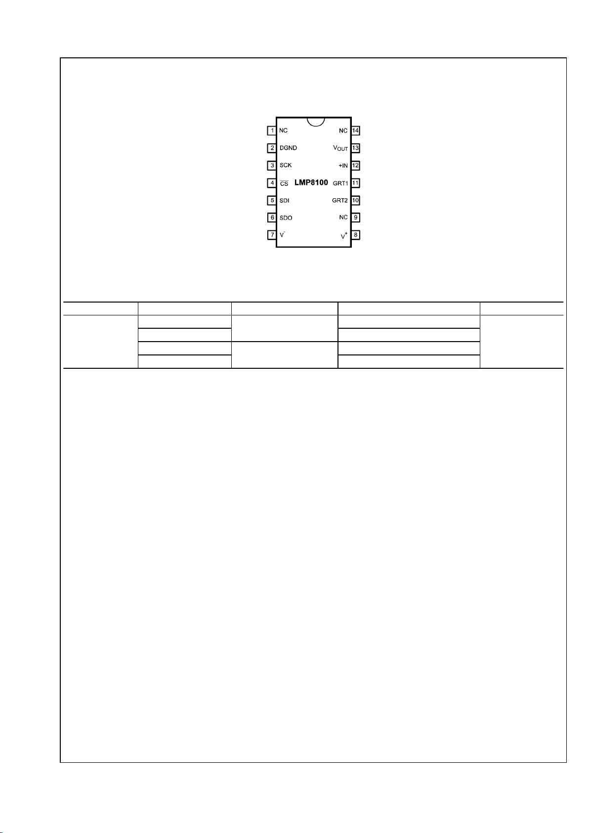
Connection Diagram
14-Pin SOIC
20147601
Top View
Ordering Information
Package Part Number Package Marking Transport Media NSC Drawing
14-Pin SOIC
LMP8100AMA
LMP8100AMA
55 Units/Rail
M14A
LMP8100AMAX 2.5k units Tape and Reel
LMP8100MA
LMP8100MA
55 Units/Rail
LMP8100MAX 2.5k units Tape and Reel
www.national.com 6
LMP8100
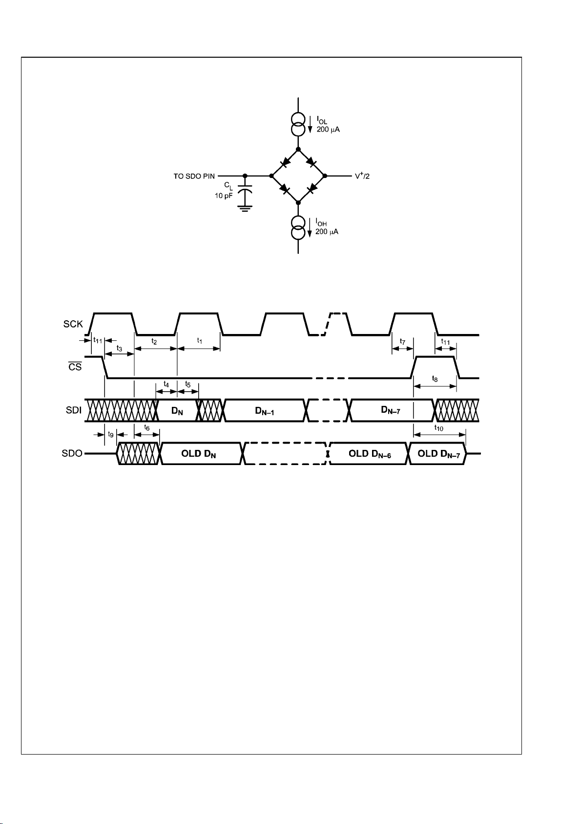
Timing Diagram Test Circuit
20147653
Timing Diagram
20147603
7 www.national.com
LMP8100
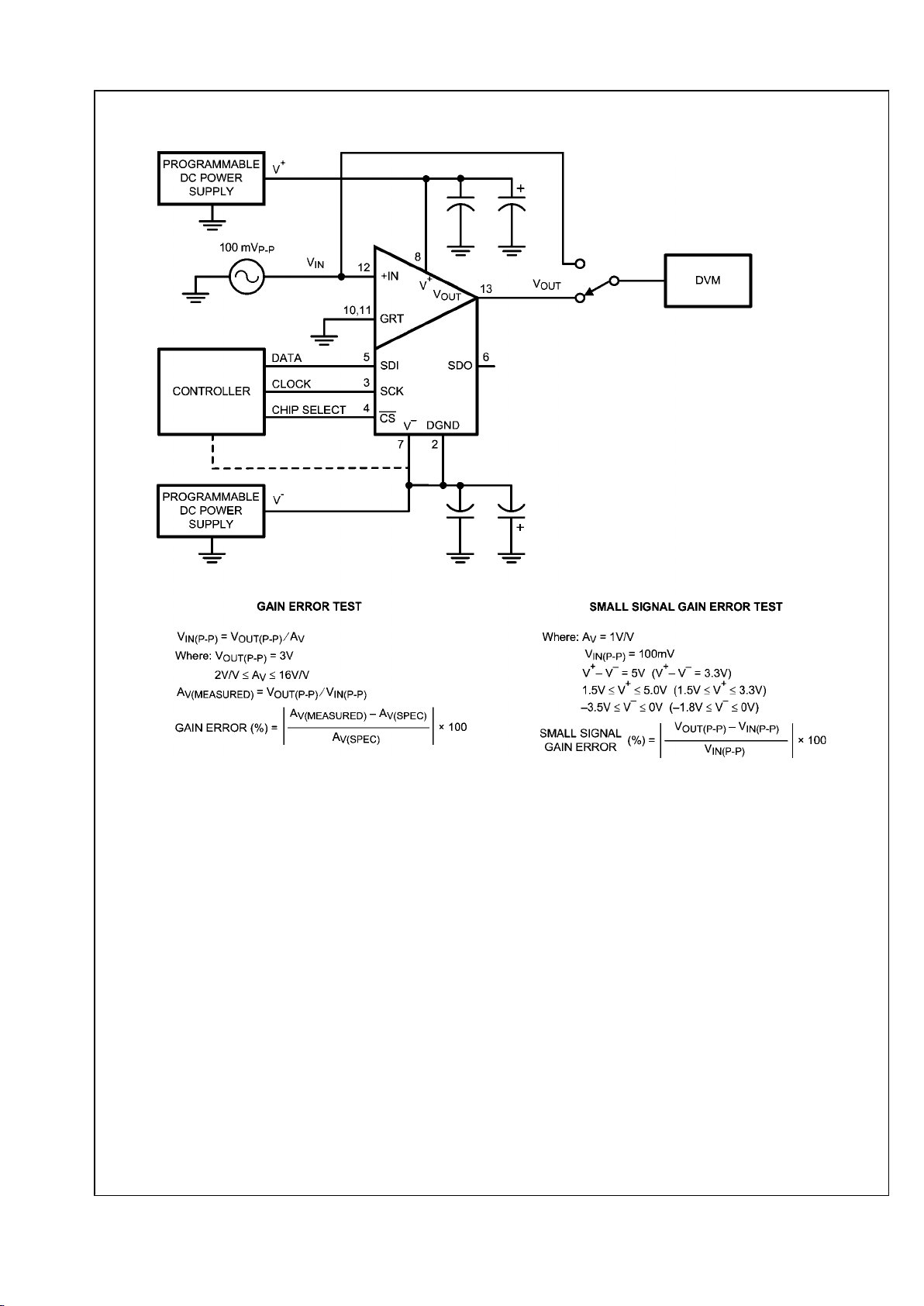
Test Circuit Diagram
20147609
Test Circuit
www.national.com 8
LMP8100
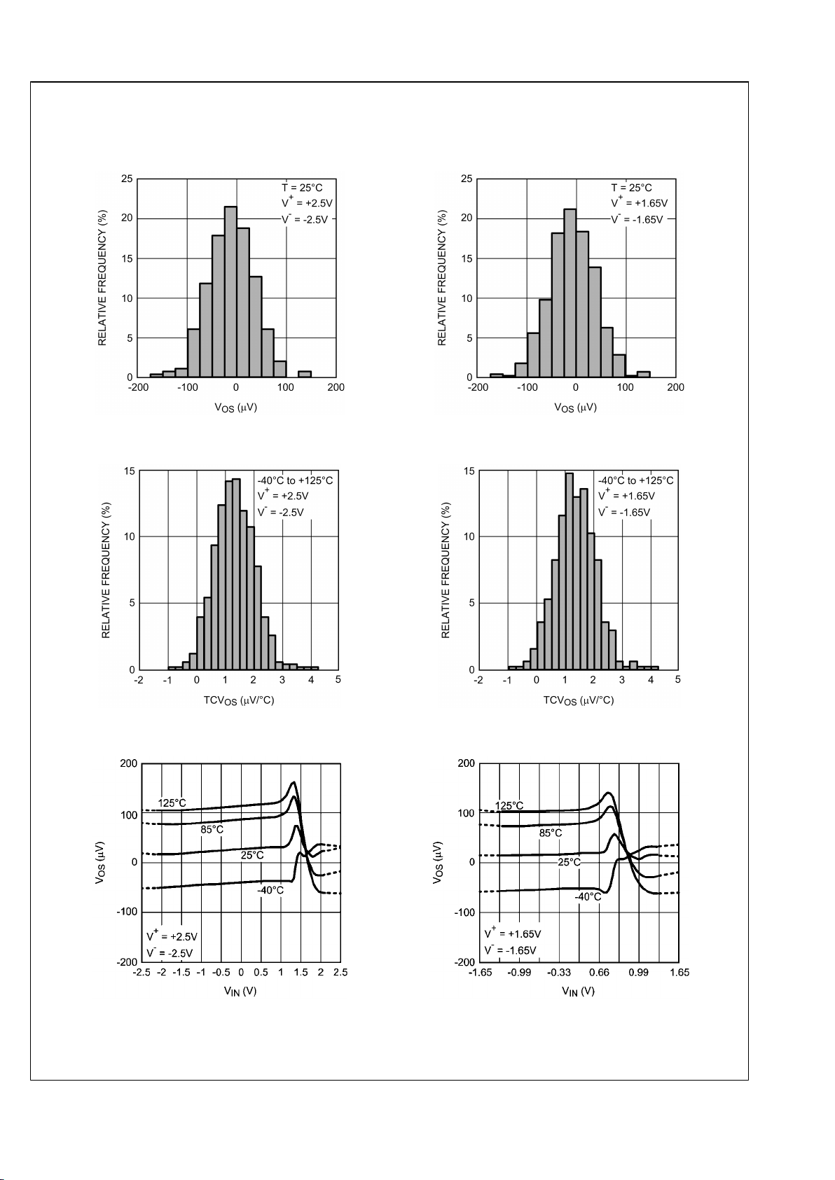
Typical Performance Characteristics
Offset Voltage Distribution
20147685
Offset Voltage Distribution
20147686
TCVOS Distribution
20147683
TCVOS Distribution
20147684
VOS vs. V
IN
20147666
VOS vs. V
IN
20147667
9 www.national.com
LMP8100
 Loading...