

NSC LMP2232BMMX, LMP2232 Datasheet
January 15, 2008
LMP2232 Dual
Micropower, 1.8V, Precision, Operational Amplifier with
CMOS Input
General Description
The LMP2232 is a dual micropower precision amplifier designed for battery powered applications. The 1.8V to 5.0V
guaranteed supply voltage range and quiescent power consumption of only 29 μW extend the battery life in portable
systems. The LMP2232 is part of the LMP® precision amplifier
family. The high impedance CMOS input makes it ideal for
instrumentation and other sensor interface applications.
The LMP2232 has a maximum offset voltage of 150 μV and
maximum offset voltage drift of only 0.5 μV/°C along with low
bias current of only ±20 fA. These precise specifications make
the LMP2232 a great choice for maintaining system accuracy
and long term stability.
The LMP2232 has a rail-to-rail output that swings 15 mV from
the supply voltage, which increases system dynamic range.
The common mode input voltage range extends 200 mV below the negative supply, thus the LMP2232 is ideal for ground
sensing in single supply applications.
The LMP2232 is offered in 8-pin SOIC and MSOP packages.
The LMP2231 is the single version of this product and the
LMP2234 is the quad version of this product. Both of these
products are available on National Semiconductor's website.
Features
(For VS = 5V, Typical unless otherwise noted)
■
Supply current (per channel) 10 µA
■
Operating voltage range 1.6V to 5.5V
■
Low TCV
OS
±0.5 µV/°C (max)
■
V
OS
±150 µV (max)
■
Input bias current 20 fA
■
PSRR 120 dB
■
CMRR 97 dB
■
Open loop gain 120 dB
■
Gain bandwidth product 130 kHz
■
Slew rate 58 V/ms
■
Input voltage noise, f = 1 kHz 60 nV/√Hz
■
Temperature range –40°C to 125°C
Applications
■
Precision instrumentation amplifiers
■
Battery powered medical instrumentation
■
High impedance sensors
■
Strain gauge bridge amplifier
■
Thermocouple amplifiers
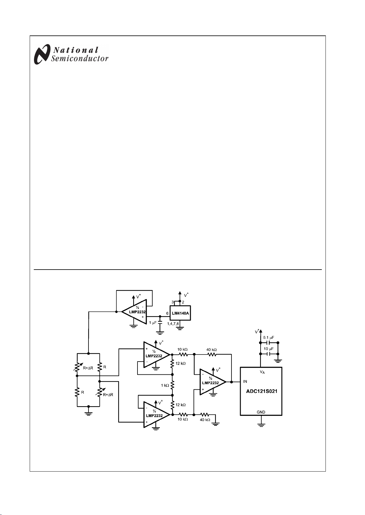
Typical Application
30033974
Strain Gauge Bridge Amplifier
LMP® is a registered trademark of National Semiconductor Corporation.
© 2008 National Semiconductor Corporation 300339 www.national.com
LMP2232 Dual 1.8V, Micropower, Precision, Operational Amplifier with CMOS Input
Absolute Maximum Ratings (Note 1)
If Military/Aerospace specified devices are required,
please contact the National Semiconductor Sales Office/
Distributors for availability and specifications.
ESD Tolerance (Note 2)
Human Body Model 2000V
Machine Model 100V
Differential Input Voltage ±300 mV
Supply Voltage (VS = V+ - V–)
6V
Voltage on Input/Output Pins V+ + 0.3V, V– – 0.3V
Storage Temperature Range −65°C to 150°C
Junction Temperature (Note 3) 150°C
Mounting Temperature
Infrared or Convection (20 sec.) +235°C
Wave Soldering Lead
Temperature (10 sec.) +260°C
Operating Ratings (Note 1)
Operating Temperature Range (Note 3) −40°C to 125°C
Supply Voltage (VS = V+ - V–)
1.6V to 5.5V
Package Thermal Resistance (θJA)(Note 3)
8-Pin SOIC 111.2 °C/W
8-Pin MSOP 147.4 °C/W
5V DC Electrical Characteristics (Note 4) Unless otherwise specified, all limits guaranteed for T
A
= 25°C,
V+ = 5V, V− = 0V, VCM = VO = V+/2, and RL > 1 MΩ. Boldface limits apply at the temperature extremes.
Symbol Parameter Conditions Min
(Note 6)
Typ
(Note 5)
Max
(Note 6)
Units
V
OS
Input Offset Voltage ±10 ±150
±230
μV
TCV
OS
Input Offset Voltage Drift LMP2232A ±0.3 ±0.5
μV/°C
LMP2232B ±0.3 ±2.5
I
BIAS
Input Bias Current 0.02 ±3
±125
pA
I
OS
Input Offset Current 5 fA
CMRR Common Mode Rejection Ratio
0V ≤ VCM ≤ 4V
81
80
97
dB
PSRR Power Supply Rejection Ratio
1.6V ≤ V+ ≤ 5.5V
V− = 0V, VCM = 0V
83
83
120
dB
CMVR Common Mode Voltage Range
CMRR ≥ 80 dB
CMRR ≥ 79 dB
−0.2
−0.2
4.2
4.2
V
A
VOL
Large Signal Voltage Gain VO = 0.3V to 4.7V
RL = 10 kΩ to V+/2
110
108
120
dB
V
O
Output Swing High
RL = 10 kΩ to V+/2
VIN(diff) = 100 mV
17 50
50
mV
from either
rail
Output Swing Low
RL = 10 kΩ to V+/2
VIN(diff) = −100 mV
17 50
50
I
O
Output Current (Note 7) Sourcing, VO to V
−
VIN(diff) = 100 mV
27
19
30
mA
Sinking, VO to V
+
VIN(diff) = −100 mV
17
12
22
I
S
Supply Current 19 27
28
μA
5V AC Electrical Characteristics (Note 4) Unless otherwise specified, all limits guaranteed for T
A
= 25°C,
V+ = 5V, V− = 0V, VCM = VO = V+/2, and RL > 1 MΩ. Boldface limits apply at the temperature extremes.
Symbol Parameter Conditions Min
(Note 6)
Typ
(Note 5)
Max
(Note 6)
Units
GBW Gain-Bandwidth Product
CL = 20 pF, RL = 10 kΩ
130 kHz
SR Slew Rate AV = +1 Falling Edge 33
32
58
V/ms
Rising Edge 33
32
48
θ
m
Phase Margin
CL = 20 pF, RL = 10 kΩ
68 deg
www.national.com 2
LMP2232
Symbol Parameter Conditions Min
(Note 6)
Typ
(Note 5)
Max
(Note 6)
Units
G
m
Gain Margin
CL = 20 pF, RL = 10 kΩ
27
dB
e
n
Input-Referred Voltage Noise Density f = 1 kHz 60
nV/
Input Referred Voltage Noise 0.1 Hz to 10 Hz 2.3
μV
PP
i
n
Input-Referred Current Noise f = 1 kHz 10
fA/
THD+N Total Harmonic Distortion + Noise
f = 100 Hz, RL = 10 kΩ
0.002
%
3.3V DC Electrical Characteristics (Note 4) Unless otherwise specified, all limits guaranteed for
T A = 25°C, V+ = 3.3V, V− = 0V, VCM = VO = V+/2, and RL > 1 MΩ. Boldface limits apply at the temperature extremes.
Symbol Parameter Conditions Min
(Note 6)
Typ
(Note 5)
Max
(Note 6)
Units
V
OS
Input Offset Voltage ±10 ±160
±250
μV
TCV
OS
Input Offset Voltage Drift LMP2232A ±0.3 ±0.5
μV/°C
LMP2232B ±0.3 ±2.5
I
BIAS
Input Bias Current 0.02 ±3
±125
pA
I
OS
Input Offset Current 5
fA
CMRR Common Mode Rejection Ratio
0V ≤ VCM ≤ 2.3V
79
77
92
dB
PSRR Power Supply Rejection Ratio
1.6V ≤ V+ ≤ 5.5V
V− = 0V, VCM = 0V
83
83
120
dB
CMVR Common Mode Voltage Range
CMRR ≥ 78 dB
CMRR ≥ 77 dB
−0.2
−0.2
2.5
2.5
V
A
VOL
Large Signal Voltage Gain VO = 0.3V to 3V
RL = 10 kΩ to V+/2
108
107
120
dB
V
O
Output Swing High
RL = 10 kΩ to V+/2
VIN(diff) = 100 mV
14 50
50
mV
from either
rail
Output Swing Low
RL = 10 kΩ to V+/2
VIN(diff) = −100 mV
14 50
50
I
O
Output Current (Note 7) Sourcing, VO to V
−
VIN(diff) = 100 mV
11
8
14
mA
Sinking, VO to V
+
VIN(diff) = −100 mV
8
5
11
I
S
Supply Current 17 25
26
μA
3.3V AC Electrical Characteristics (Note 4) Unless otherwise is specified, all limits guaranteed for
TA = 25°C, V+ = 3.3V, V− = 0V, VCM = VO = V+/2, and RL > 1 MΩ. Boldface limits apply at the temperature extremes.
Symbol Parameter Conditions Min
(Note 6)
Typ
(Note 5)
Max
(Note 6)
Units
GBW Gain-Bandwidth Product
CL = 20 pF, RL = 10 kΩ
128 kHz
SR Slew Rate AV = +1, CL = 20 pF
RL = 10 kΩ
Falling Edge 58
V/ms
Rising Edge 48
θ
m
Phase Margin
CL = 20 pF, RL = 10 kΩ
66 deg
G
m
Gain Margin
CL = 20 pF, RL = 10 kΩ
26 dB
e
n
Input-Referred Voltage Noise Density f = 1 kHz 60
nV/
Input-Referred Voltage Noise 0.1 Hz to 10 Hz 2.4
μV
PP
3 www.national.com
LMP2232
Symbol Parameter Conditions Min
(Note 6)
Typ
(Note 5)
Max
(Note 6)
Units
i
n
Input-Referred Current Noise f = 1 kHz 10
fA/
THD+N Total Harmonic Distortion + Noise
f = 100 Hz, RL = 10 kΩ
0.003
%
2.5V DC Electrical Characteristics (Note 4) Unless otherwise specified, all limits guaranteed for
TA = 25°C, V+ = 2.5V, V− = 0V, VCM = VO = V+/2, and RL > 1MΩ. Boldface limits apply at the temperature extremes.
Symbol Parameter Conditions Min
(Note 6)
Typ
(Note 5)
Max
(Note 6)
Units
V
OS
Input Offset Voltage ±10 ±190
±275
μV
TCV
OS
Input Offset Voltage Drift LMP2232A ±0.3 ±0.5
μV/°C
LMP2232B ±0.3 ±2.5
I
Bias
Input Bias Current 0.02 ±3
±125
pA
I
OS
Input Offset Current 5
fA
CMRR Common Mode Rejection Ratio
0V ≤ VCM ≤ 1.5V
77
76
91
dB
PSRR Power Supply Rejection Ratio
1.6V ≤ V+ ≤ 5.5V
V– = 0V, VCM = 0V
83
83
120
dB
CMVR Common Mode Voltage Range
CMRR ≥ 77 dB
CMRR ≥ 76 dB
−0.2
−0.2
1.7
1.7
V
A
VOL
Large Signal Voltage Gain VO = 0.3V to 2.2V
RL = 10 kΩ to V+/2
104
104
120
dB
V
O
Output Swing High
RL = 10 kΩ to V+/2
VIN(diff) = 100 mV
12 50
50
mV
from either
rail
Output Swing Low
RL = 10 kΩ to V+/2
VIN(diff) = –100 mV
13 50
50
I
O
Output Current (Note 7) Sourcing, VO to V
–
VIN(diff) = 100 mV
5
4
8
mA
Sinking, VO to V
+
VIN(diff) = –100 mV
3.5
2.5
7
I
S
Supply Current 16 24
25
µA
2.5V AC Electrical Characteristics (Note 4) Unless otherwise specified, all limits guaranteed for
TA = 25°C, V+ = 2.5V, V− = 0V, VCM = VO = V+/2, and RL > 1MΩ. Boldface limits apply at the temperature extremes.
Symbol Parameter Conditions Min
(Note 6)
Typ
(Note 5)
Max
(Note 6)
Units
GBW Gain-Bandwidth Product
CL = 20 pF, RL = 10 kΩ
128 kHz
SR Slew Rate AV = +1, CL = 20 pF
RL = 10 kΩ
Falling Edge 58
V/ms
Rising Edge 48
θ
m
Phase Margin
CL = 20 pF, RL = 10 kΩ
64 deg
G
m
Gain Margin
CL = 20 pF, RL = 10 kΩ
26
dB
e
n
Input-Referred Voltage Noise Density f = 1 kHz 60
nV/
Input-Referred Voltage Noise 0.1 Hz to 10 Hz 2.5
μV
PP
i
n
Input-Referred Current Noise f = 1 kHz 10
fA/
THD+N Total Harmonic Distortion + Noise
f = 100 Hz, RL = 10 kΩ
0.005 %
www.national.com 4
LMP2232
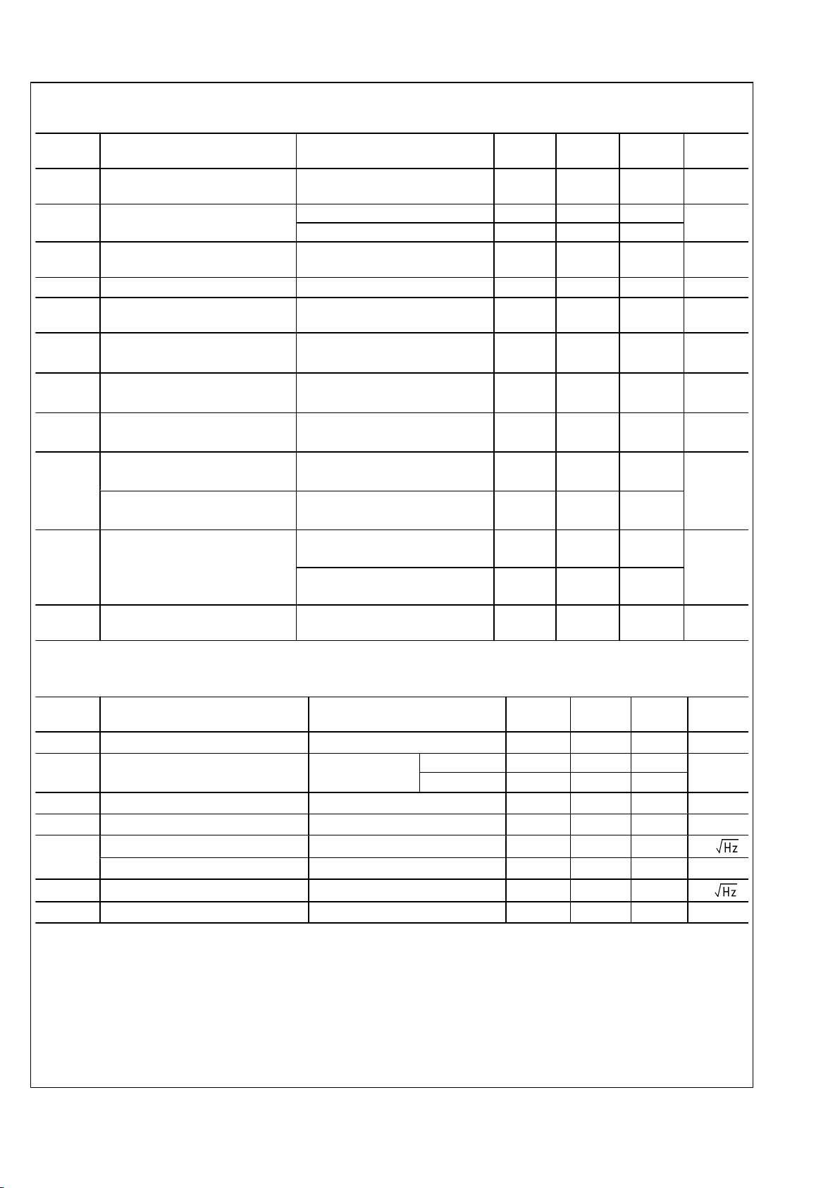
1.8V DC Electrical Characteristics (Note 4) Unless otherwise specified, all limits guaranteed for
T A = 25°C, V+ = 1.8V, V− = 0V, VCM = VO = V+/2, and RL > 1 MΩ. Boldface limits apply at the temperature extremes.
Symbol Parameter Conditions Min
(Note 6)
Typ
(Note 5)
Max
(Note 6)
Units
V
OS
Input Offset Voltage ±10 ±230
±325
μV
TCV
OS
Input Offset Voltage Drift LMP2232A ±0.3 ±0.5
μV/°C
LMP2232B ±0.3 ±2.5
I
BIAS
Input Bias Current 0.02 ±3
±125
pA
I
OS
Input Offset Current 5 fA
CMRR Common Mode Rejection Ratio
0V ≤ VCM ≤ 0.8V
76
75
92
dB
PSRR Power Supply Rejection Ratio
1.6V ≤ V+ ≤ 5.5V
V− = 0V, VCM = 0V
83
83
120
dB
CMVR Common Mode Voltage Range
CMRR ≥ 76 dB
CMRR ≥ 75 dB
−0.2
0
1.0
1.0
V
A
VOL
Large Signal Voltage Gain VO = 0.3V to 1.5V
RL = 10 kΩ to V+/2
103
103
120
dB
V
O
Output Swing High
RL = 10 kΩ to V+/2
VIN(diff) = 100 mV
12 50
50
mV
from either
rail
Output Swing Low
RL = 10 kΩ to V+/2
VIN(diff) = −100 mV
13 50
50
I
O
Output Current (Note 7) Sourcing, VO to V
–
VIN(diff) = 100 mV
2.5
2
5
mA
Sinking, VO to V
+
VIN(diff) = −100 mV
2
1.5
5
I
S
Supply Current 16 24
25
µA
1.8V AC Electrical Characteristics (Note 4) Unless otherwise is specified, all limits guaranteed for
TA = 25°C, V+ = 1.8V, V− = 0V, VCM = VO = V+/2, and RL > 1 MΩ. Boldface limits apply at the temperature extremes.
Symbol Parameter Conditions Min
(Note 6)
Typ
(Note 5)
Max
(Note 6)
Units
GBW Gain-Bandwidth Product
CL = 20 pF, RL = 10 kΩ
127 kHz
SR Slew Rate AV = +1, CL = 20 pF
RL = 10 kΩ
Falling Edge 58
V/ms
Rising Edge 48
θ
m
Phase Margin
CL = 20 pF, RL = 10 kΩ
60 deg
G
m
Gain Margin
CL = 20 pF, RL = 10 kΩ
25
dB
e
n
Input-Referred Voltage Noise Density f = 1 kHz 60
nV/
Input-Referred Voltage Noise 0.1 Hz to 10 Hz 2.4
μV
PP
i
n
Input-Referred Current Noise f = 1 kHz 10
fA/
THD+N Total Harmonic Distortion + Noise
f = 100 Hz, RL = 10 kΩ
0.005 %
5 www.national.com
LMP2232
Note 1: Absolute Maximum Ratings indicate limits beyond which damage may occur. Operating Ratings indicate conditions for which the device is intended to
be functional, but specific performance is not guaranteed. For guaranteed specifications and test conditions, see the Electrical Characteristics.
Note 2: Human Body Model, applicable std. MIL-STD-883, Method 3015.7. Machine Model, applicable std. JESD22-A115-A (ESD MM std. of JEDEC)
Field-Induced Charge-Device Model, applicable std. JESD22-C101-C (ESD FICDM std. of JEDEC).
Note 3: The maximum power dissipation is a function of T
J(MAX)
, θJA, and TA. The maximum allowable power dissipation at any ambient temperature is
PD = (T
J(MAX)
– TA)/ θJA. All numbers apply for packages soldered directly onto a PC board.
Note 4: Electrical Table values apply only for factory testing conditions at the temperature indicated. Factory testing conditions result in very limited self-heating
of the device such that TJ = TA. No guarantee of parametric performance is indicated in the electrical tables under conditions of internal self-heating where TJ >
TA. Absolute Maximum Ratings indicate junction temperature limits beyond which the device may be permanently degraded, either mechanically or electrically.
Note 5: Typical values represent the most likely parametric norm at the time of characterization. Actual typical values may vary over time and will also depend
on the application and configuration. The typical values are not tested and are not guaranteed on shipped production material.
Note 6: All limits are guaranteed by testing, statistical analysis or design.
Note 7: The short circuit test is a momentary open loop test.
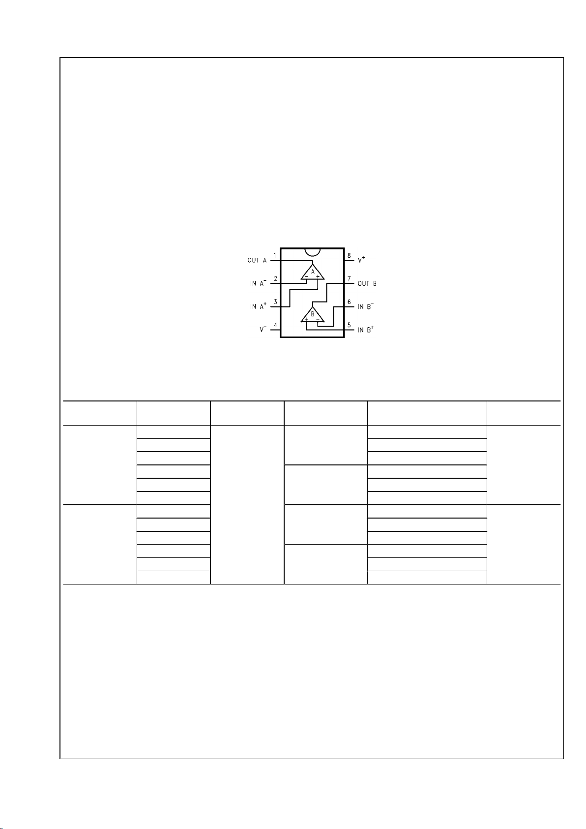
Connection Diagram
8-Pin MSOP/SOIC
30033938
Top View
Ordering Information
Package Part Number Temperature
Range
Package Marking Transport Media NSC Drawing
8-Pin SOIC
LMP2232AMA
–40°C to 125°C
LMP2232AMA
95 Units/Rail
M08A
LMP2232AMAE 250 Units Tape and Reel
LMP2232AMAX 2.5k Units Tape and Reel
LMP2232BMA
LMP2232BMA
95 Units/Rail
LMP2232BMAE 250 Units Tape and Reel
LMP2232BMAX 2.5k Units Tape and Reel
8-Pin MSOP
LMP2232AMM
AK5A
1k Units Tape and Reel
MUA08A
LMP2232AMME 250 Units Tape and Reel
LMP2232AMMX 3.5k Units Tape and Reel
LMP2232BMM
AK5B
1k Units Tape and Reel
LMP2232BMME 250 Units Tape and Reel
LMP2232BMMX 3.5k Units Tape and Reel
www.national.com 6
LMP2232
 Loading...