NSC LMK01020ISQX, LMK01000 Datasheet
March 6, 2008
LMK01000/LMK01010/LMK01020
1.6 GHz High Performance Clock Buffer, Divider, and
Distributor
General Description
The LMK01000/LMK01010/LMK01020 family provides an
easy way to divide and distribute high performance clock signals throughout the system. These devices provide best-inclass noise performance and are designed to be pin-to-pin
and footprint compatible with LMK03000/LMK02000 family of
precision clock conditioners.
The LMK01000/LMK01010/LMK01020 family features two
programmable clock inputs (CLKin0 and CLKin1) that allow
the user to dynamically switch between different clock domains.
Each device features 8 clock outputs with independently programmable dividers and delay adjustments. The outputs of
the device can be easily synchronized by an external pin
(SYNC*).
Target Applications
■
High performance Clock Distribution
■
Wireless Infrastructure
■
Medical Imaging
■
Wired Communications
■
Test and Measurement
■
Military / Aerospace
Features
■
30 fs additive jitter (100 Hz to 20 MHz)
■
Dual clock inputs
■
Programmable output channels (0 to 1600 MHz)
—
LMK01000: 3 LVDS outputs (CLKout0 - CLKout2) + 5
LVPECL outputs (CLKout3 - CLKout7)
—
LMK01010: 8 LVDS outputs
—
LMK01020: 8 LVPECL outputs
—
Channel divider values of 1, 2 to 510 (even divides)
—
Programmable output skew control
■
External synchronization
■
Pin compatible family of clocking devices
■
3.15 to 3.45 V operation
■
Package: 48 pin LLP (7.0 x 7.0 x 0.8 mm)
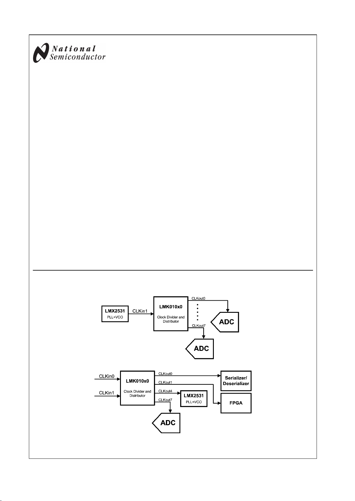
System Diagram
30042806
TRI-STATE® is a registered trademark of National Semiconductor Corporation.
© 2008 National Semiconductor Corporation 300428 www.national.com
LMK01000/LMK01010/LMK01020 1.6 GHz High Performance Clock Buffer, Divider, and
Distributor
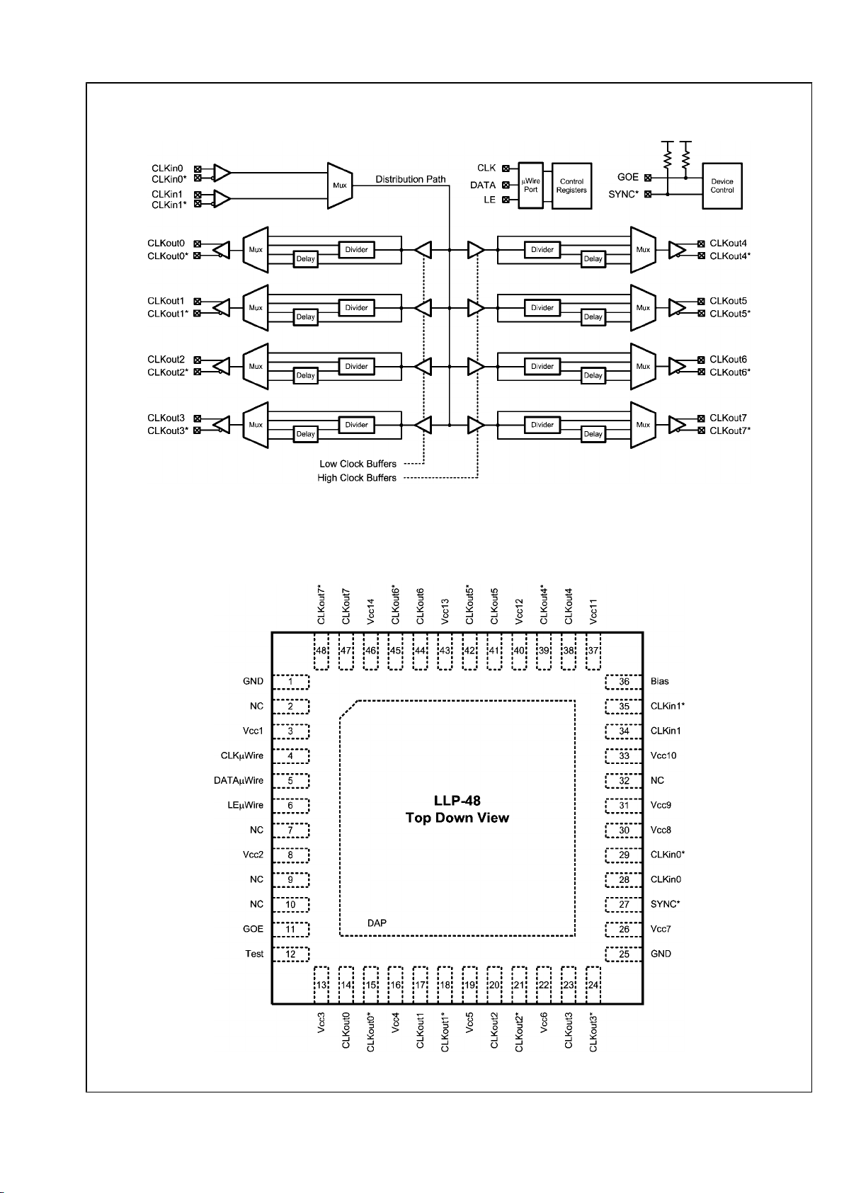
Functional Block Diagram
30042801
Connection Diagram
48-Pin LLP Package
30042802
www.national.com 2
LMK01000/LMK01010/LMK01020

Pin Descriptions
Pin # Pin Name I/O Description
1, 25 GND - Ground
2, 7, 9,10, 32 NC - No Connect. Pin is not connected to the die.
3, 8, 13, 16, 19, 22, 26,
30, 31, 33, 37, 40, 43, 46
Vcc1, Vcc2, Vcc3, Vcc4, Vcc5, Vcc6, Vcc7,
Vcc8, Vcc9, Vcc10, Vcc11, Vcc12, Vcc13, Vcc14
- Power Supply
4 CLKuWire I MICROWIRE Clock Input
5 DATAuWire I MICROWIRE Data Input
6 LEuWire I MICROWIRE Latch Enable Input
11 GOE I Global Output Enable
12 Test O
This is an output pin used strictly for test purposes
and should be not connected for normal operation.
However, any load of an impedance of more than 1
kΩ is acceptable.
14, 15 CLKout0, CLKout0* O Clock Output 0
17, 18 CLKout1, CLKout1* O Clock Output 1
20, 21 CLKout2, CLKout2* O Clock Output 2
23, 24 CLKout3, CLKout3* O Clock Output 3
27 SYNC* I Global Clock Output Synchronization
28, 29 CLKin0,CLKin0* I CLKin 0 Input; Must be AC coupled
34, 35 CLKin1, CLKin1* I CLKin 1 Input; Must be AC coupled
36 Bias I Bias Bypass
38, 39 CLKout4, CLKout4* O Clock Output 4
41, 42 CLKout5, CLKout5* O Clock Output 5
44, 45 CLKout6, CLKout6* O Clock Output 6
47, 48 CLKout7, CLKout7* O Clock Output 7
DAP DAP - Die Attach Pad should be connected to ground.
The LMK01000 family is footprint compatible with the LMK03000/02000 family of devices. All CLKout pins are pin-to-pin compatible,
and CLKin0 and CLKin1 are equivalent to OSCin and Fin, respectively .
3 www.national.com
LMK01000/LMK01010/LMK01020
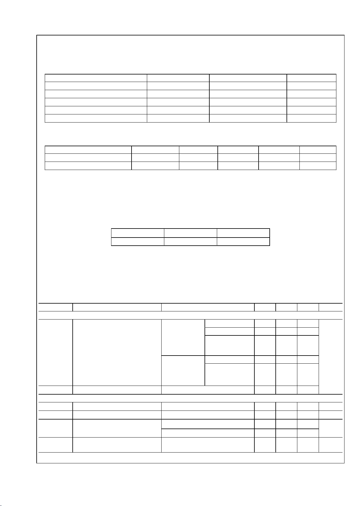
Absolute Maximum Ratings (Notes 1, 2)
If Military/Aerospace specified devices are required, please contact the National Semiconductor Sales Office/ Distributors
for availability and specifications.
Parameter Symbol Ratings Units
Power Supply Voltage
V
CC
-0.3 to 3.6 V
Input Voltage
V
IN
-0.3 to (VCC + 0.3)
V
Storage Temperature Range
T
STG
-65 to 150 °C
Lead Temperature (solder 4 s)
T
L
+260 °C
Junction Temperature
T
J
125 °C
Recommended Operating Conditions
Parameter Symbol Min Typ Max Units
Ambient Temperature
T
A
-40 25 85 °C
Power Supply Voltage
V
CC
3.15 3.3 3.45 V
Note 1: "Absolute Maximum Ratings" indicate limits beyond which damage to the device may occur, including inoperability and degradation of device reliability
and/or performance. Functional operation of the device and/or non-degradation at the Absolute Maximum Ratings or other conditions beyond those indicated in
the Recommended Operating Conditions is not implied. The Recommended Operating Conditions indicate conditions at which the device is functional and the
device should not be operated beyond such conditions.
Note 2: This device is a high performance integrated circuit with ESD handling precautions. Handling of this device should only be done at ESD protected work
stations. The device is rated to a HBM-ESD of > 2 kV, a MM-ESD of > 200 V, and a CDM-ESD of > 1.2 kV.
Package Thermal Resistance
Package
θ
JA
θ
J-PAD (Thermal Pad)
48-Lead LLP (Note 3) 27.4° C/W 5.8° C/W
Note 3: Specification assumes 16 thermal vias connect the die attach pad to the embedded copper plane on the 4-layer JEDEC board. These vias play a key
role in improving the thermal performance of the LLP. It is recommended that the maximum number of vias be used in the board layout.
Electrical Characteristics (Note 4)
(3.15 V ≤ Vcc ≤ 3.45 V, -40 °C ≤ TA ≤ 85 °C, Differential Inputs/Outputs; except as specified. Typical values represent most likely
parametric norms at Vcc = 3.3 V, TA = 25 °C, and at the Recommended Operation Conditions at the time of product characterization
and are not guaranteed).
Symbol Parameter Conditions Min Typ Max Units
Current Consumption
I
CC
Power Supply Current
(Note 5)
All outputs
enabled, no
divide or delay
( CLKoutX_MUX
= Bypassed )
LMK01000 271
mA
LMK01010 160
LMK01020 338
Per channel, no
divide or delay
(CLKoutX_MUX
= Bypassed )
LVDS 17.8
LVPECL
(Includes Emitter
Resistors)
40
ICCPD
Power Down Current POWERDOWN = 1 1
CLKin0, CLKin0*, CLKin1, CLKin1*
f
CLKin
CLKin Frequency Range 1 1600 MHz
SLEW
CLKin
CLKin Frequency Input Slew Rate (Notes 6, 8) 0.5 V/ns
DUTY
CLKin
CLKin Frequency Input Duty Cycle
f
CLKin
≤ 800 MHz
30 70
%
f
CLKin
> 800 MHz
40 60
P
CLKin
Input Power Range for CLKin or
CLKin*
AC coupled -13 5 dBm
www.national.com 4
LMK01000/LMK01010/LMK01020
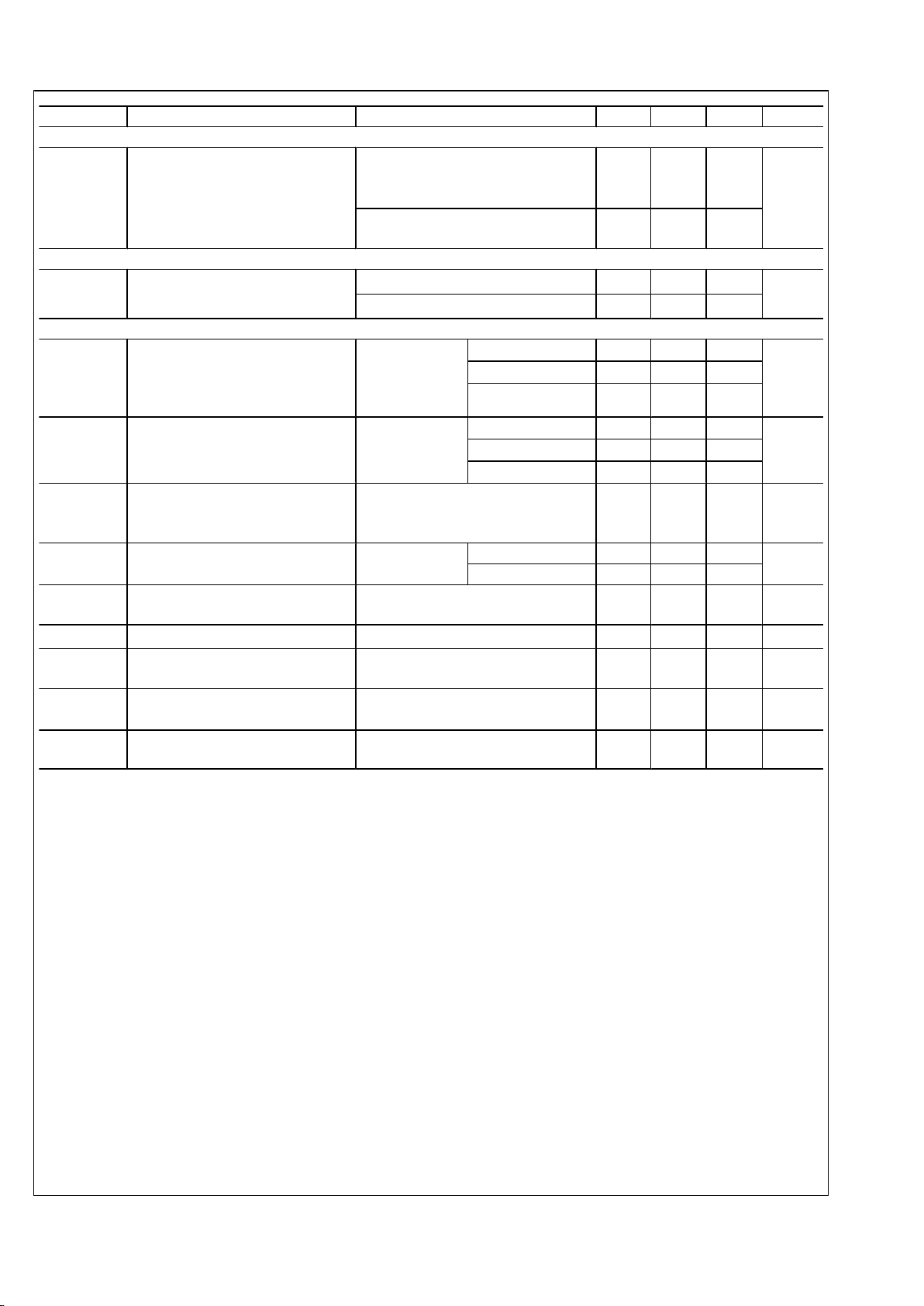
Symbol Parameter Conditions Min Typ Max Units
Clock Distribution Section--Delays
Delay
CLKout
Maximum Allowable Delay(Note 8)
f
CLKoutX
≤ 1 GHz
(Delay is limited to maximum
programmable value)
2250
ps
f
CLKoutX
> 1 GHz
(Delay is limited to 1/2 of a period)
0.5/
f
CLKoutX
Clock Distribution Section - Divides
Divide
CLKoutX
Allowable divide range. (Note that 1 is
the only allowable odd divide value)
f
CLKinX
≤ 1300 MHz
1 510
n/a
1300 MHz < f
CLKinX
≤ 1600 MHz
1 2
Clock Distribution Section - LVDS Clock Outputs
Jitter
ADD
Additive RMS Jitter (Note 7)
RL = 100 Ω
Bandwidth =
100 Hz to 20 MHz
Vboost = 1
f
CLKoutX
= 200 MHz
80
fs
f
CLKoutX
= 800 MHz
30
f
CLKoutX
= 1600 MHz
25
Noise Floor Divider Noise Floor(Note 7)
RL = 100
Vboost = 1
f
CLKoutX
= 200 MHz
-156
dBc/Hz
f
CLKoutX
= 800 MHz
-153
f
CLKoutX
= 1600 MHz
-148
t
SKEW
CLKoutX to CLKoutY (Note 8)
Equal loading and identical clock
configuration
RL = 100 Ω
-30 ±4 30 ps
V
OD
Differential Output Voltage (Note 9)
Vboost=0 250 350 450
mV
Vboost=1 390
ΔV
OD
Change in magnitude of VOD for
complementary output states
RL = 100 Ω
-50 50 mV
V
OS
Output Offset Voltage
RL = 100 Ω
1.070 1.25 1.370 V
ΔV
OS
Change in magnitude of VOS for
complementary output states
RL = 100 Ω
-35 35 mV
I
SA
I
SB
Clock Output Short Circuit Current
single ended
Single ended outputs shorted to GND -24 24 mA
I
SAB
Clock Output Short Circuit Current
differential
Complementary outputs tied together -12 12 mA
5 www.national.com
LMK01000/LMK01010/LMK01020
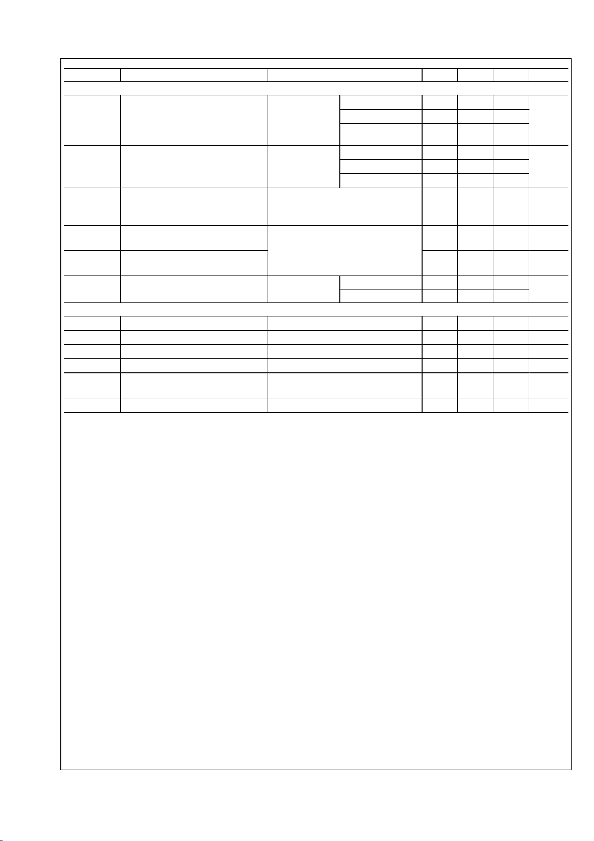
Symbol Parameter Conditions Min Typ Max Units
Clock Distribution Section - LVPECL Clock Outputs
Jitter
ADD
Additive RMS Jitter(Note 7)
RL = 100 Ω
Bandwidth =
100 Hz to 20 MHz
Vboost = 1
f
CLKoutX
= 200 MHz
65
fs
f
CLKoutX
= 800 MHz
25
f
CLKoutX
= 1600 MHz
25
Noise Floor Divider Noise Floor(Note 7)
RL = 100
Vboost = 1
f
CLKoutX
= 200 MHz
-158
dBc/Hz
f
CLKoutX
= 800 MHz
-154
f
CLKoutX
= 1600 MHz
-148
t
SKEW
CLKoutX to CLKoutY (Note 8)
Equal loading and identical clock
configuration
Termination = 50 Ω to Vcc - 2 V
-30 ±3 30 ps
V
OH
Output High Voltage
Termination = 50 Ω to Vcc - 2 V
Vcc -
0.98
V
V
OL
Output Low Voltage
Vcc -
1.8
V
V
OD
Differential Output Voltage (Note 9)
Vboost = 0 660 810 965
mV
Vboost = 1 865
Digital LVTTL Interfaces (Note 10)
V
IH
High-Level Input Voltage 2.0 Vcc V
V
IL
Low-Level Input Voltage 0.8 V
I
IH
High-Level Input Current
VIH = Vcc
-5.0 5.0 µA
I
IL
Low-Level Input Current
VIL = 0
-40.0 5.0 µA
V
OH
High-Level Output Voltage
IOH = +500 µA
Vcc -
0.4
V
V
OL
Low-Level Output Voltage
IOL = -500 µA
0.4 V
www.national.com 6
LMK01000/LMK01010/LMK01020
 Loading...