NSC LMH7220MK, LMH7220 Datasheet
LMH7220
High Speed Comparator with LVDS Output
LMH7220 High Speed Comparator with LVDS Output
April 2007
General Description
The LMH7220 is a high speed, low power comparator with an
operating supply voltage range of 2.7V to 12V. The LMH7220
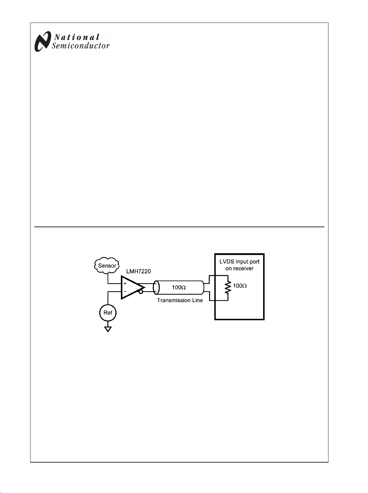
has a differential, LVDS output, driving 325 mV into a 100Ω
symmetrical transmission line. The LMH7220 has a 2.9 ns
propagation delay and 0.6 ns rise and fall times while the
supply current is only 6.8 mA at 5V (load current excluded).
The LMH7220 inputs have a voltage range that extends 200
mV below ground, allowing ground sensing applications. The
LMH7220 is available in the 6-Pin TSOT package. ThIs package is ideal where space is a critical item.
Typical Schematic
Features
(VS = 5V TA = 25°C, Typical values unless otherwise specified)
Propagation delay @ 100 mV overdrive 2.9 ns
■
Rise and fall times 0.6 ns
■
Supply voltage 2.7V to 12V
■
Supply current 6.8 mA
■
Temperature range −40°C to 125°C
■
LVDS output
■
Applications
Acquisition trigger
■
Fast differential line receiver
■
Pulse height analyzer
■
Peak detector
■
Pulse width modulator
■
Remote threshold detection
■
Oscilloscope triggering
■
20137603
© 2007 National Semiconductor Corporation 201376 www.national.com
Absolute Maximum Ratings (Note 1)
If Military/Aerospace specified devices are required,
please contact the National Semiconductor Sales Office/
LMH7220
Distributors for availability and specifications.
ESD Tolerance (Note 2)
Human Body Model 2.5 kV
Machine Model 250V
Supply Voltage (VCC - GND)
Differential Input Voltage ±13V
Output Shorted to GND (Note 4) Continuous
13.5V
Output Shorted Together (Note 4) Continuous
Storage Temperature Range −65°C to +150°C
Voltage on any I/O Pin GND−0.2V to VCC+0.2V
Junction Temperature (Note 3) 150°C max
Operating Ratings (Note 1)
Temperature Range (Note 3) −40°C to +125°C
Supply Voltage 2.7V to 13V
Package Thermal Resistance (θJA )
6-Pin TSOT 189°C/W
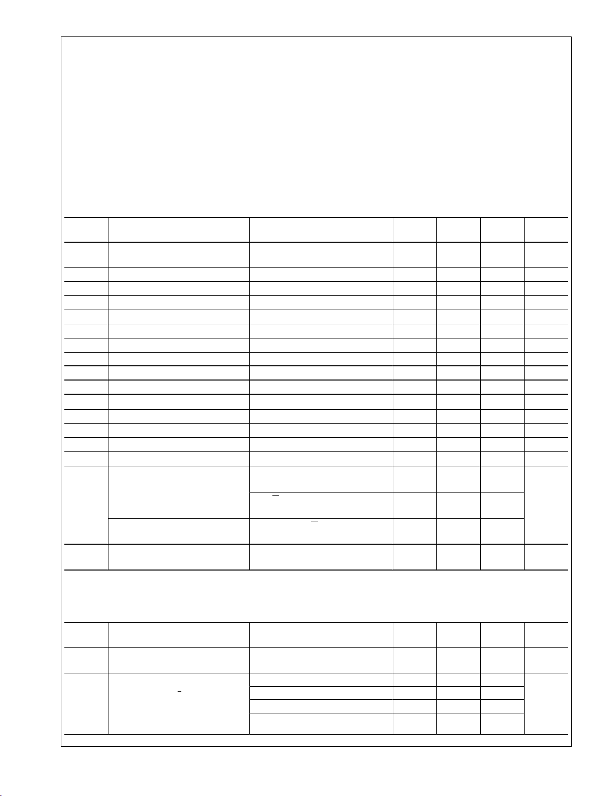
+12V DC Electrical Characteristics
Unless otherwise specified, all limits are guaranteed for TJ = 25°C, VCM = 300 mV, −50 mV < VID < +50 mV and RL = 100Ω.
Boldface limits apply at the temperature extremes. (Note 6)
Symbol Parameter Conditions Min
(Note 6)
I
B
Input Bias Current VIN Differential = 0 −5
−7
I
OS
TC I
V
OS
TC V
Input Offset Current VIN Differential = 0 −500 +500 nA
Input Offset Current TC VIN Differential = 0 ±2 nA/°C
OS
Input Offset Voltage −9.5 +9.5 mV
Input Offset Voltage TC ± 50
OS
VRI Input Voltage Range CMRR > 50 dB −0.2 VCC−2 V
CMRR Common-Mode Rejection Ratio VCM = 0 to VCC−2.2V 60 70 dB
PSRR Power Supply Rejection Ratio 63 74 dB
A
V
ΔV
V
V
V
ΔV
I
SC
I
S
V
O
O
OH
OL
OD
OD
Open Loop Gain 59 dB
Output Offset Voltage VIN Differential = 50 mV 1125 1225 1325 mV
VO Change Between ‘0’ and ‘1’ VIN Differential = ±50 mV −25 +25 mV
Output Voltage High VIN Differential = 50 mV 1390 1475 mV
Output Voltage Low VIN Differential = 50 mV 925 1060 mV
Output Voltage Differential VIN Differential = 50 mV 250 330 400 mV
VOD Change between ‘0’ to ‘1’ VIN Differential = ±50 mV −25 +25 mV
Short Circuit Current Output to GND
Pin (Note 4)
Output Shorted Together (Note 4) OUT Q to OUT Q
Supply Current Load Current Excluded
OUT Q to GND Pin
VIN Differential = 50 mV
OUT Q to GND Pin
V
Differential = 50 mV
IN
V
Differential = 50 mV
IN
V
Differential = 50 mV
IN
5
5
5
7.5 10.0
Typ
(Note 5)
(Note 6)
−2.1 −0.5
Max
14.0
Units
µA
μV/°C
mA
mA
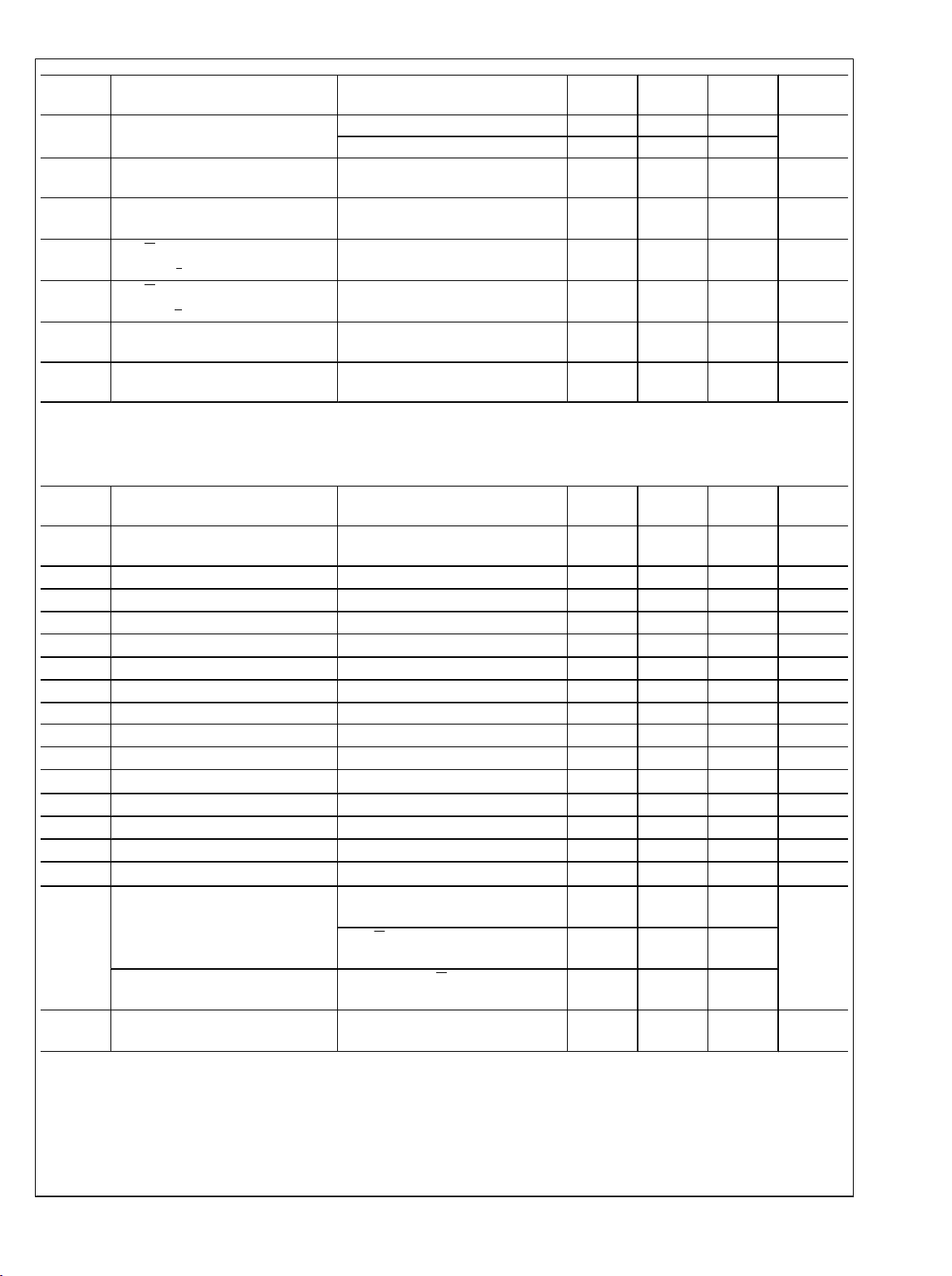
+12V AC Electrical Characteristics
Unless otherwise specified, all limits guaranteed for TJ = 25°C, VCM = 300 mV, −50 mV < VID < +50 mV and RL = 100Ω. Boldface limits apply at the temperature extremes. (Note 6)
Symbol Parameter Conditions Min
TR Toggle Rate Overdrive = ±50 mV; CL = 2 pF @
50% Output Swing
t
PDLH
www.national.com 2
Propagation Delay
t
= (t
+ t
PDLH
PDH
PDL
) / 2
(see figure 3 application note)
Input SR = Constant
VID start value = −100 mV
Overdrive 20 mV 3.56
Overdrive 50 mV 2.98
Overdrive 100 mV 2.7 7
Overdrive 1V 2.24
(Note 6)
860 1080 Mb/s
Typ
(Note 5)
Max
(Note 6)
Units
ns
LMH7220
Symbol Parameter Conditions Min
(Note 6)
tOD-disp Input Overdrive Dispersion @Overdrive 20 - 100 mV 0.86
@Overdrive 100 mV - 1V 0.46
tSR-disp Input Slew Rate Dispersion 0.05 V/ns to 1 V/ns
0.24 ns
Typ
(Note 5)
Max
(Note 6)
Units
ns
Overdrive 100 mV
tCM-disp Input Common Mode dispersion SR = 4 V/ns; Overdrive 100 mV
0.55 ns
VCM = 0 to 10V
Δt
Δt
t
t
r
f
PDLH
PDHL
Q to Q Time Skew
| t
- t
PDH
| (Note 8)
PDL
Q to Q Time Skew
| t
- t
PDL
| (Note 8)
PDH
Output Rise Time (20% - 80%) (Note9)Overdrive = 100 mV; CL = 2 pF 0.56 ns
Output Fall Time (20% - 80%) (Note9)Overdrive = 100 mV; CL = 2 pF 0.49 ns
Overdrive = 100 mV; CL = 2 pF 0 ns
Overdrive = 100 mV; CL = 2 pF 0.06 ns
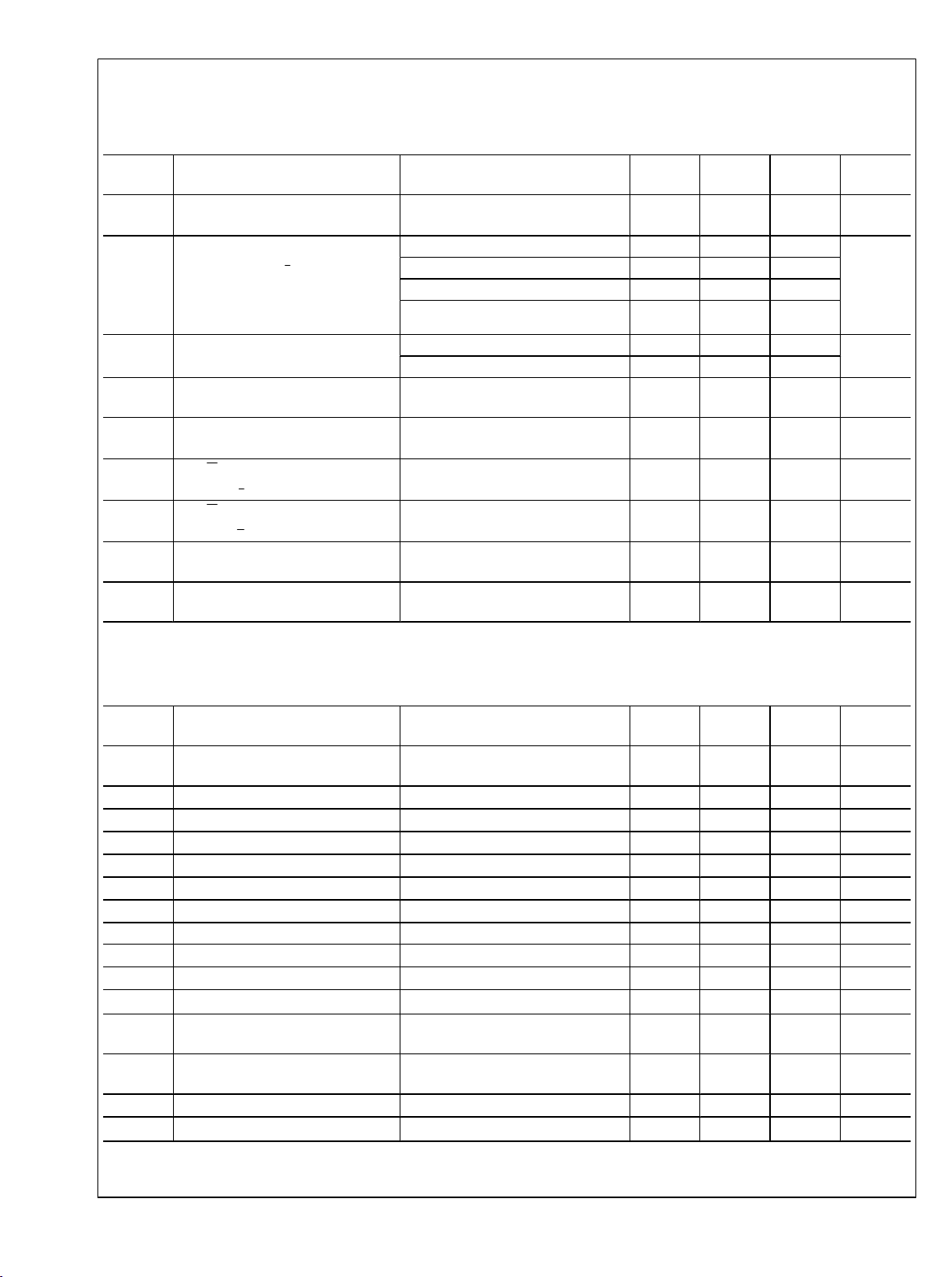
+5V DC Electrical Characteristics
Unless otherwise specified, all limits guaranteed for TJ = 25°C, VCM = 300 mV, −50 mV < VID < +50 mV and RL = 100Ω. Boldface limits apply at the temperature extremes. (Note 6)
Symbol Parameter Conditions Min
(Note 6)
I
B
Input Bias Current VIN Differential = 0 −5
−7
I
OS
TC I
V
OS
TC V
Input Offset Current VIN Differential = 0 −500 +500 nA
Input Offset Current TC VIN Differential = 0 ± 2 nA/°C
OS
Input Offset Voltage −9.5 +9.5 mV
Input Offset Voltage TC ± 50
OS
VRI Input Voltage Range CMRR > 50 dB −0.2 VCC−2 V
CMRR Common-Mode Rejection Ratio VCM = 0 to VCC−2.2V 60 70 dB
PSRR Power Supply Rejection Ratio 63 74 dB
A
V
ΔV
V
V
V
ΔV
I
SC
I
S
V
O
O
OH
OL
OD
OD
Open Loop Gain 59 dB
Output Offset Voltage VIN Differential = 50 mV 1125 1217 1325 mV
VO Change Between ‘0’ and ‘1’ VIN Differential = ±50 mV −25 +25 mV
Output Voltage High VIN Differential = 50 mV 1380 1475 mV
Output Voltage Low VIN Differential = 50 mV 925 1060 mV
Output Voltage Differential VIN Differential = 50 mV 250 320 400 mV
VOD Change between ‘0’ to ‘1’ VIN Differential = ±50 mV −25 +25 mV
Short Circuit Current Output to GND
Pin (Note 4)
Output Shorted Together (Note 4) OUT Q to OUT Q
Supply Current Load Current Excluded
OUT Q to GND Pin
VIN Differential = 50 mV
OUT Q to GND Pin
V
Differential = 50 mV
IN
V
Differential = 50 mV
IN
V
Differential = 50 mV
IN
5
5
5
6.8 9
Typ
(Note 5)
(Note 6)
−1.5 −0.5
Max
12.6
Units
µA
μV/°C
mA
mA
3 www.national.com
+5V AC Electrical Characteristics
Unless otherwise specified, all limits guaranteed for TJ = 25°C, VCM = 300 mV, −50 mV < VID < +50 mV and RL = 100Ω. Bold-
LMH7220
face limits apply at the temperature extremes. (Note 6)
Symbol Parameter Conditions Min
(Note 6)
TR Toggle Rate Overdrive = ±50 mV; CL = 2 pF @
750 940 Mb/s
50% Output Swing
t
PDLH
Propagation Delay
t
= (t
+ t
PDLH
PDH
PDL
) / 2
(see figure 3 application note)
Input SR = Constant
VID start value = -100mV
Overdrive 20 mV 3.63
Overdrive 50 mV 3.09
Overdrive 100 mV 2.9 7
Overdrive 1V 2.41
tOD-disp Input Overdrive Dispersion @Overdrive 20 - 100 mV 0.79
@Overdrive 100 mV - 1V 0.43
tSR-disp Input Slew Rate Dispersion 0.05 V/ns to 1 V/ns
0.20 ns
Overdrive 100 mV
tCM-disp Input Common Mode Dispersion SR = 4 V/ns; Overdrive 100 mV
0.21 ns
VCM = 0 to 3V
Δt
Δt
t
r
PDLH
PDHL
Q to Q Time Skew
| t
- t
PDH
| (Note 8)
PDL
Q to Q Time Skew
| t
- t
PDL
| (Note 8)
PDH
Output Rise Time (20% - 80%) (Note9)Overdrive = 100 mV; CL = 2 pF 0.59 ns
Overdrive = 100 mV; CL = 2 pF 0.09 ns
Overdrive = 100 mV; CL = 2 pF 0.07 ns
Typ
(Note 5)
Max
(Note 6)
Units
ns
ns
t
f
Output Fall Time (20% - 80%) (Note9)Overdrive = 100 mV; CL = 2 pF 0.55 ns
+2.7V DC Electrical Characteristics
Unless otherwise specified, all limits guaranteed for TJ = 25°C, VCM = 300 mV, −50 mV < VID < +50 mV and RL = 100Ω. Boldface limits apply at the temperature extremes. (Note 6)
Symbol Parameter Conditions Min
(Note 6)
I
B
Input Bias Current VIN Differential = 0 −5
−7
I
OS
TC I
V
OS
TC V
Input Offset Current VIN Differential = 0 −500 +500 nA
Input Offset Current TC VIN Differential = 0 ±2 nA/°C
OS
Input Offset Voltage −9.5 +9.5 mV
Input Offset Voltage TC ± 50
OS
VRI Input Voltage Range CMRR > 50 dB −0.2 VCC−2 V
CMRR Common-Mode Rejection Ratio VCM = 0 to VCC−2.2V 56 70 dB
PSRR Power Supply Rejection Ratio 63 74 dB
A
V
ΔV
V
V
O
O
OH
Open Loop Gain 59 dB
Output Offset Voltage VIN Differential = 50 mV 1125 1213 1325 mV
VO Change Between ‘0’ and ‘1’ VIN Differential = ± 50 mV −25 +25 mV
Output Voltage High
VIN Differential = 50 mV 1370 1475 mV
Average of ‘0’ to ‘1’
V
OL
Output Voltage Low
VIN Differential = 50 mV 925 1060 mV
Average of ‘0’ to ‘1’
V
ΔV
OD
OD
Output Voltage Differential VIN Differential = 50 mV 250 315 400 mV
VOD Change between ‘0’ to ‘1’ VIN Differential = ±50 mV −25 +25 mV
Typ
(Note 5)
(Note 6)
−1.3 −0.5
Max
Units
µA
μV/°C
www.national.com 4
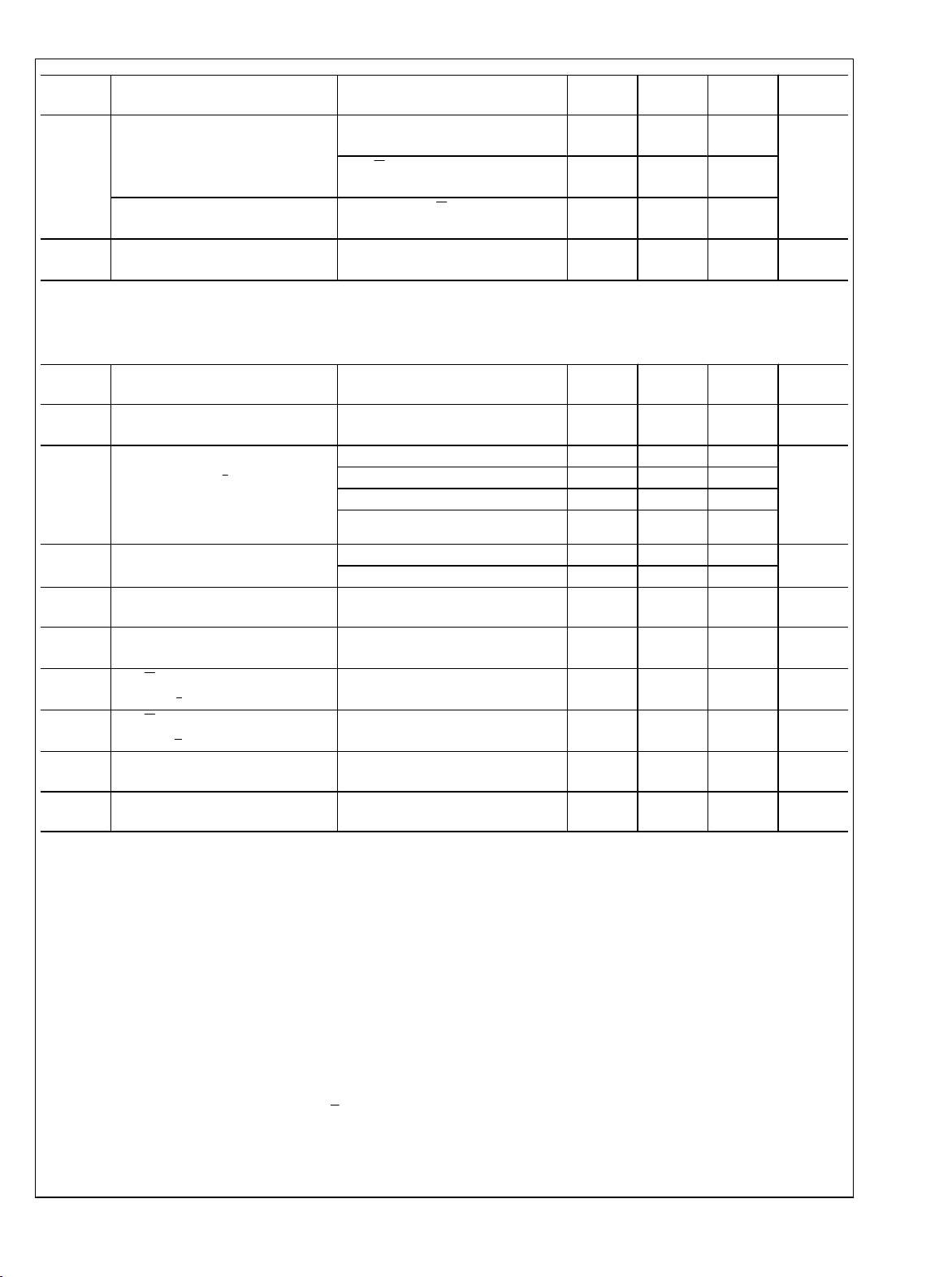
LMH7220
Symbol Parameter Conditions Min
(Note 6)
I
SC
Short Circuit Current Output to GND
Pin (Note 4)
OUT Q to GND Pin
VIN Differential = 50 mV
OUT Q to GND Pin
V
Differential = 50 mV
IN
Output Shorted Together (Note 4) OUT Q to OUT Q
V
Differential = 50 mV
IN
I
S
Supply Current Load Current Excluded
V
Differential = 50 mV
IN
5
5
5
6.6 9
Typ
(Note 5)
Max
(Note 6)
12.6
+2.7V AC Electrical Characteristics
Unless otherwise specified, all limits guaranteed for TJ = 25°C, VCM = 300 mV, −50 mV < VID < +50 mV and RL = 100Ω. Boldface limits apply at the temperature extremes. (Note 6)
Symbol Parameter Conditions Min
(Note 6)
TR Toggle Rate Overdrive = ±50 mV; CL = 2 pF @
700 880 Mb/s
50% Output Swing
t
PDLH
Propagation Delay
t
= (t
+ t
PDLH
PDH
PDL
) / 2
(see figure 3 application note)
Input SR = Constant
VID start value = -100mV
Overdrive 20 mV 3.80
Overdrive 50 mV 3.29
Overdrive 100 mV 3.0 7
Overdrive 1V 2.60
tOD-disp Input Overdrive Dispersion @Overdrive 20 - 100 mV 0.83
@Overdrive 100 mV - 1V 0.37
tSR-disp Input Slew Rate Dispersion 0.05 V/ns to 1 V/ns
0.23 ns
Overdrive 100 mV
tCM-disp Input Common Mode dispersion SR = 4 V/ns; Overdrive 100 mV
0.16 ns
VCM = 0 to 1.5V
Δt
PDLH
ΔtPDHL
t
r
Q to Q Time Skew
| t
- t
PDH
| (Note 8)
PDL
Q to Q Time Skew
| t
- t
PDL
| (Note 8)
PDH
Output Rise Time (20% - 80%) (Note9)Overdrive = 100 mV; CL = 2 pF 0.64 ns
Overdrive = 100 mV; CL = 2 pF 0.09 ns
Overdrive = 100 mV; CL = 2 pF 0.09 ns
Typ
(Note 5)
Max
(Note 6)
Units
mA
mA
Units
ns
ns
t
f
Note 1: Absolute Maximum Ratings indicate limits beyond which damage to the device may occur. Operating Conditions indicate specifications for which the
device is intended to be functional, but specific performance is not guaranteed. For guaranteed specifications and the test conditions, see the Electrical
Characteristics.
Note 2: Human Body Model, applicable std. MIL-STD-883, Method 3015.7. Machine Model, applicable std. JESD22-A115-A (ESD MM std. of JEDEC)
Field-Induced Charge-Device Model, applicable std. JESD22-C101-C (ESD FICDM std. of JEDEC)
Note 3: The maximum power dissipation is a function of T
PD = (T
Note 4: Applies to both single-supply and split-supply operation. Continuous short circuit operation at elevated ambient temperature can result in exceeding the
maximum allowed junction temperature of 150°C.
Note 5: Typical values represent the most likely parametric norm as determined at the time of characterization. Actual typical values may vary over time and will
also depend on the application and configuration. The typical values are not tested and are not guaranteed on shipped production material.
Note 6: All limits are guaranteed by testing or statistical analysis.
Note 7: Electrical Table values apply only for factory testing conditions at the temperature indicated. Factory testing conditions result in very limited self-heating
of the device such that TJ = TA. No guarantee of parametric performance is indicated in the electrical tables under conditions of internal self heating where TJ >
TA. See applications section for information on temperature de-rating of this device.
Note 8: Propagation Delay Skew, ΔtPD, is defined as the average of Δt
Note 9: The rise or fall time is the average of the Q and Q
Output Fall Time (20% - 80%) (Note9)Overdrive = 100 mV; CL = 2 pF 0.59 ns
, θJA. The maximum allowable power dissipation at any ambient temperature is
– TA)/ θJA. All numbers apply for packages soldered directly onto a PC Board.
J(MAX)
J(MAX)
PDLH
rise or fall time.
and Δt
.
PDHL
5 www.national.com
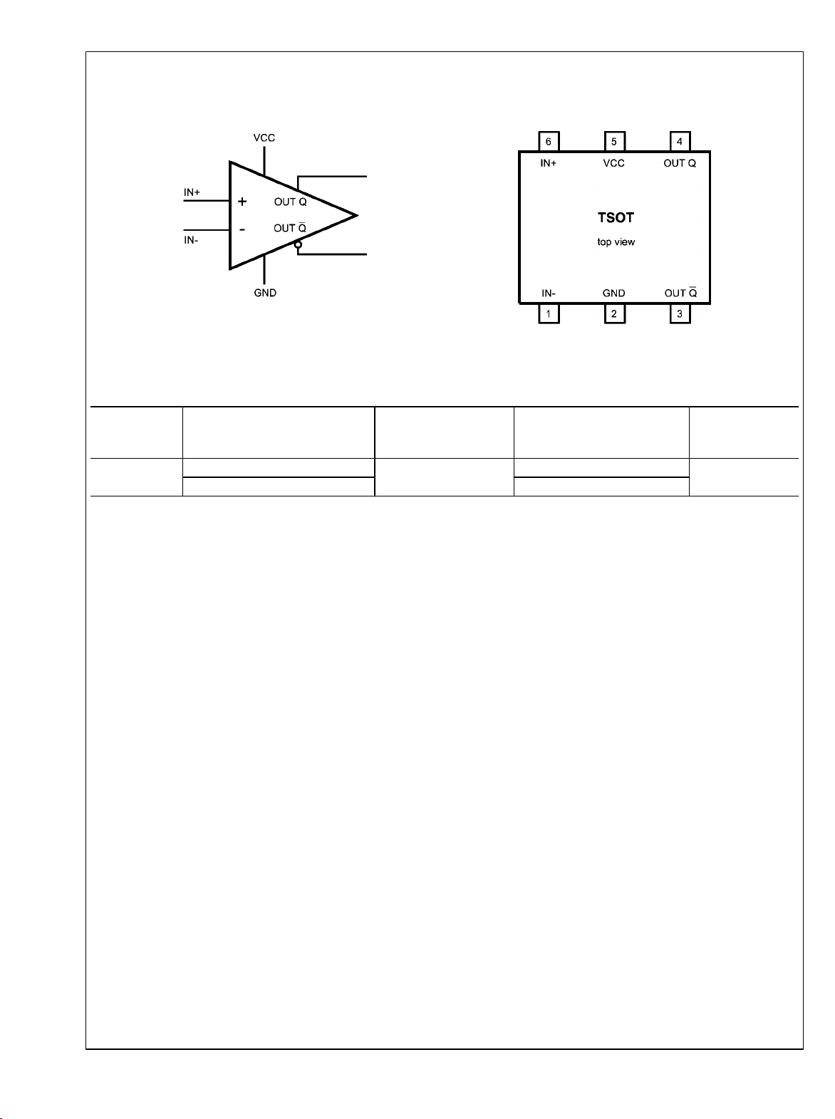
Diagrams
LMH7220
Schematic Diagram
Ordering Information
Package Part Number
Temperature Range (TA)
6-Pin TSOT
Connection Diagram
20137601
Package Marking Transport Media NSC Drawing
−40°C to +85°C
LMH7220MK
LMH7220MKX 3k Units Tape and Reel
C29A
1k Units Tape and Reel
20137602
MK06A
www.national.com 6
 Loading...