

LMH6718
Dual, High Output, Programmable Gain Buffer
General Description
The LMH6718 is a dual, low cost high speed (130MHz)
buffer which features user programmable gains of +2, +1,
and -1V/V. The LMH6718 also has a new output stage that
delivers high output drive current (200mA), but consumes
minimal quiescent supply current (2.6mA/Amp) from a
±
5V
supply. Its current feedback architecture, fabricated in an
advanced complementary bipolar process, maintains consistent performance over a wide range of signal levels, and has
a linear phase response up to one half of the -3dB frequency.
The LMH6718 offers 0.1dB gain flatness to 30MHz and
differential gain and phase errors of .04% and .03˚. These
features are ideal for professional and consumer video applications.
The LMH6718 offers superior dynamic performance with a
130MHz small-signal bandwidth, 600V/µs slew rate and
4.2ns rise/fall times (2V
STEP
). The combination of low quiescent current, high output current drive, and high speed performance makes the LMH6718 well suited for many battery
powered personal communication/computing systems. The
ability to drive low impedance, high capacitive loads, makes
the LMH6718 ideal for single ended cable applications. It
also drives low impedance loads with minimum distortion.
The LMH6718 will drive a 100Ω load with only −84/−84dBc
second/third harmonic distortion (A
V
= +2, V
OUT
=2VPP,f=
1MHz). It is also optimized for driving high currents into
single-ended transformers and coils. When driving the input
of high resolution A/D converters, the LMH6718 provides
excellent -88/-98dBc second/third harmonic distortion (A
V
=
+2, V
OUT
=2VPP, f = 1MHz, RL=1kΩ) and fast settling time.
The LMH6718 is fabricated using National’s VIP10
™
com-
plimentary bipolar process.
Features
n 200mA output current
n .04%, .03˚ differential gain, phase
n 5.2mA supply current for 2 amplifiers
n 130MHz bandwidth (A
V
= +2)
n −88/−98dBc HD2/HD3 (1MHz)
n 16ns settling to 0.05%
n 600V/µs slew rate
n Nominal supply range
±
2.5V to±6V
n Improved replacement for CLC5632
Applications
n Video line driver
n Coaxial cable driver
n Twisted pair driver
n Transformer/coil driver
n High capacitive load driver
n Portable/battery powered applications
n A/D driver
n I/Q Channel Amplifier
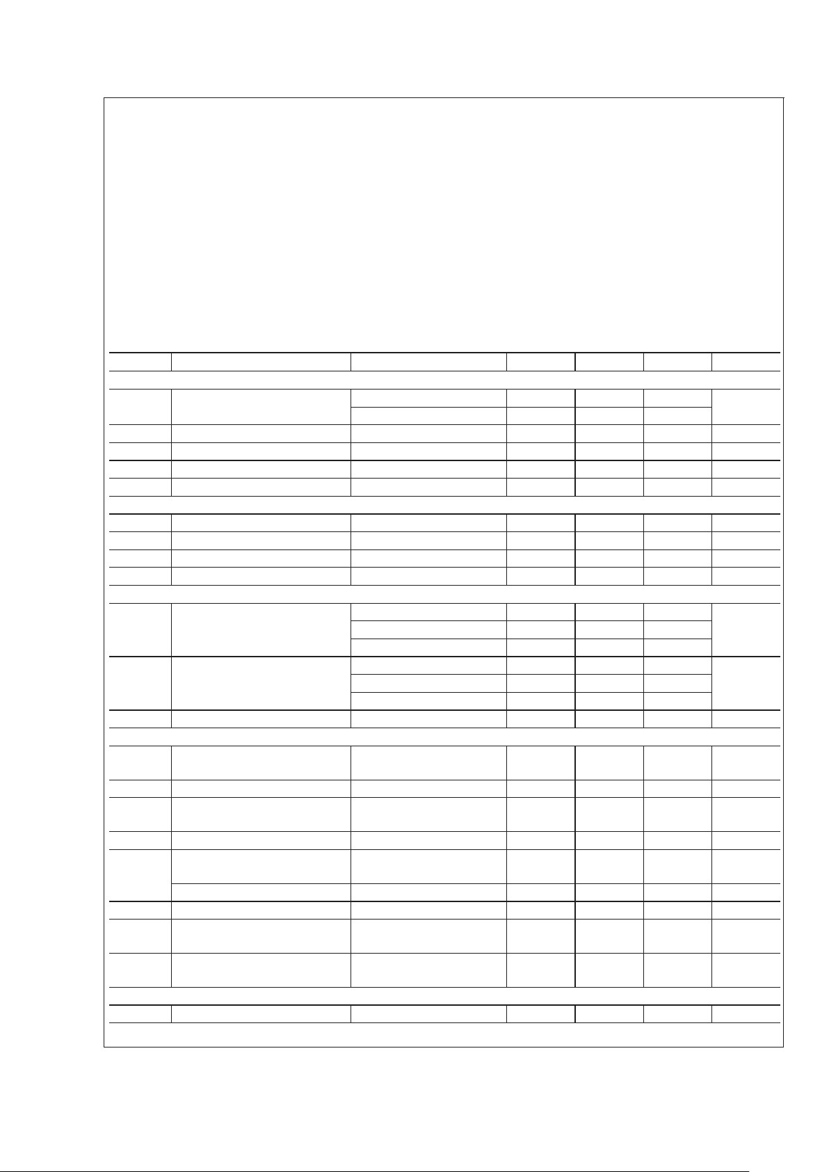
Connection Diagram
8-Pin SOIC
20040116
Top View
Maximum Output Voltage vs. Load
Resistance
20040164
January 2003
LMH6718 Dual, High Output, Programmable Gain Buffer
© 2003 National Semiconductor Corporation DS200401 www.national.com
Absolute Maximum Ratings (Note 1)
If Military/Aerospace specified devices are required,
please contact the National Semiconductor Sales Office/
Distributors for availability and specifications.
ESD Tolerance (Note 5)
Human Body Model 2kV
Machine Model 200V
Supply Voltage 13.5
Output Current (Note 3)
Common-Mode Input Voltage V
+-V−
Maximum Junction Temperature +150˚C
Storage Temperature Range −65˚C to +150˚C
Lead Temperature (Soldering 10 sec) +300˚C
Operating Ratings
Thermal Resistance
Package (θ
JC
)(θJA)
SOIC 50˚C/W 145˚C/W
Nominal Operating Voltage
±
2.5V to±6V
Operating Temperature Range −40˚C to +85˚C
+5V Electrical Characteristics (Note 2)
AV= +2, RL= 100Ω,VS= +5V (Note 4), Unless Specified. Boldface limits apply at the temperature extremes.
Symbol Parameter Conditions Min Typ Max Units
Frequency Domain Response
SSBW -3dB Bandwidth V
O
=0.5V
PP
70 110
MHz
V
O
=2.0V
PP
90
SSBW −0.1dB Bandwidth V
O
=0.5V
PP
23 MHz
GFP Gain Peaking
<
200MHz, VO=0.5V
PP
0dB
GFR Gain Rolloff
<
30MHz, VO=0.5V
PP
0.2 dB
LPD Linear Phase Deviation
<
30MHz, VO= 0.5V
PP
0.12 deg
Time Domain Response
Tr Rise and Fall Time 2V Step 4.8 ns
Ts Settling Time to 0.05% 1V Step 20 ns
OS Overshoot 2V Step 5 %
SR Slew Rate 2V Step 250 400 V/µs
Distortion And Noise Response
HD2 2nd Harmonic Distortion 2V
PP
, 1MHz −85
dBc2V
PP
, 1MHz; RL=1kΩ −88
2V
PP
, 5MHz −73
HD3 3rd Harmonic Distortion 2V
PP
,1MHz −89
dBc2V
PP
, 1MHz, RL=1kΩ −91
2V
PP
, 5MHz −71
XTLKA Crosstalk (Input Referred) 10MHz, 1V
PP
−85 dB
Static, DC Performance
V
IO
Input Offset Voltage
±
.6
±
10
±
20
mV
DV
IO
Average Drift 10 µV/˚C
I
BN
Input Bias Current
(Non-Inverting)
±
.6
±
15
±
20
µA
DI
BN
Average Drift 20 nA/˚C
GACC Gain Accuracy
±
0.3
±
1.5
±
2.0
%
Internal Resistors (R
F,RG
) 750 950 1150 Ω
PSRR Power supply Rejection Ratio DC 50 60 dB
CMRR Common Mode Rejection Ratio DC 50
47
56
dB
I
CC
Supply Current per channel RL=
∞
2.0
1.9
2.4 3.0
3.1
mA
Miscellaneous Performance
R
IN
Input Resistance (Non-Inverting) 0.38 MΩ
LMH6718
www.national.com 2
+5V Electrical Characteristics (Note 2) (Continued)
AV= +2, RL= 100Ω,VS= +5V (Note 4), Unless Specified. Boldface limits apply at the temperature extremes.
Symbol Parameter Conditions Min Typ Max Units
C
IN
Input Capacitance
(Non-Inverting)
2.2 pF
V
CMH
Input Voltage Range, High 4.2 V
V
CML
Input Voltage Range, Low 0.8 V
V
ROH
Output Voltage Range, High RL= 100Ω 3.6
3.5
4.0
V
V
ROL
Output Voltage Range, Low RL= 100Ω 1.4
1.3
1.0
V
V
ROH
Output Voltage Range, High RL=
∞
4.1 V
V
ROL
Output Voltage Range, Low RL=
∞
0.9 V
I
O
Output Current (Note 3) 170 mA
R
O
Output Resistance, Closed Loop DC .28 Ω
±
5V Electrical Characteristics (Note 2)
AV= +2, RL= 100Ω,VCC=±5V; Unless Specified. Boldface limits apply at the temperature extremes.
Symbol Parameter Conditions Min Typ Max Units
Frequency Domain Response
SSBW -3dB Bandwidth V
O
=1.0V
PP
100 130
MHz
V
O
=4.0V
PP
70
SSBW −0.1dB Bandwidth V
O
= 1.0V
PP
30 MHz
GFP Gain Peaking
<
200MHz, VO= 1.0V
PP
0dB
GFR Gain Rolloff
<
300MHz, VO= 1.0V
PP
0.1 dB
LPD Linear Phase Deviation
<
30MHz, VO= 1.0V
PP
0.1 deg
DG Differential Gain NTSC, R
L
= 150Ω .04 %
DP Differential Phase NTSC, R
L
= 150Ω .03 deg
Time Domain Response
Tr Rise and Fall Time 2V Step 4.2 ns
Ts Settling Time to 0.05% 2V Step 17 ns
OS Overshoot 2V Step 14 %
SR Slew Rate 2V Step 400 600 V/µs
Distortion And Noise Response
HD2 2nd Harmonic Distortion 2V
PP
,1MHz −84
dBc2V
PP
, 1MHz; RL=1kΩ −88
2V
PP
, 5MHz −73
HD3 3rd Harmonic Distortion 2V
PP
,1MHz −84
dBc2V
PP
, 1MHz; RL=1kΩ −98
2V
PP
, 5MHz −76
Equivalent Input Noise
V
N
Voltage (eni)
>
1MHz 8 nV/
I
NN
Non-Inverting Current (ibn)
>
1MHz 9 pA/
XTLKA Crosstalk (Input Referred) 10MHz, 1V
PP
−85 dB
Static, DC Performance
V
IO
Input Offset Voltage .2
±
9.5
±
15
mV
DV
IO
Average Drift 5 µV/˚C
I
BN
Input Bias Current
(Non-Inverting)
1.3
±
15
±
20
µA
DI
BN
Average Drift 12 nA/˚C
LMH6718
www.national.com3
±
5V Electrical Characteristics (Note 2) (Continued)
AV= +2, RL= 100Ω,VCC=±5V; Unless Specified. Boldface limits apply at the temperature extremes.
Symbol Parameter Conditions Min Typ Max Units
GACC Gain Accuracy
±
0.3
±
1.5
±
2.0
%
Internal Resistor (R
F,RG
) 750 950 1150 Ω
PSRR Power Supply Rejection Ratio DC 50 62 dB
CMRR Common Mode Rejection Ratio DC 52
49
57
dB
I
CC
Supply Current per channel RL=
∞
2.2
2.1
2.6 3.3
3.4
mA
Miscellaneous Performance
R
IN
Input Resistance (Non-Inverting) 0.50 MΩ
C
IN
Input Capacitance
(Non-Inverting)
1.9 pF
CMVR Common-Mode Voltage Range
±
4.2 V
V
RO
Output Voltage Range RL= 100Ω 3.6
3.5
±
3.8
V
V
RO
Output Voltage Range RL=
∞
±
4.0 V
I
O
Output Current (Note 3) 200 mA
R
O
Output Resistance, Closed Loop DC .28 Ω
Note 1: Absolute Maximum Ratings indicate limits beyond which damage to the device may occur. Operating Ratings indicate conditions for which the device is
intended to be functional, but specific performance is not guaranteed. For guaranteed specifications, see the Electrical Characteristics tables.
Note 2: Electrical Table values apply only for factory testing conditions at the temperature indicated. Factory testing conditions result in very limited self-heating of
the device such that T
J=TA
. No guarantee of parametric performance is indicated in the electrical tables under conditions of internal self heating where T
J
>
TA.
See Applications Section for information on temperature de-rating of this device." Min/Max ratings are based on product characterization and simulation. Individual
parameters are tested as noted.
Note 3: The maximum current is determined by device power dissipation limitations. See the Power Dissipation section of the Application Division for more details.
Note 4: V
S=VCC−VEE
Note 5: Human body model, 1.5kΩ in series with 100pF. Machine model, 0Ω In series with 200pF.
Ordering Information
Package Part Number Package Marking Transport Media NSC Drawing
8-pin SOIC LMH6718MA LMH6718MA Rails M08A
LMH6718IMAX 2.5k Units Tape and Reel
LMH6718
www.national.com 4
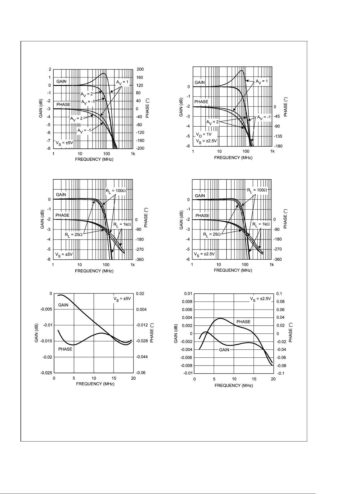
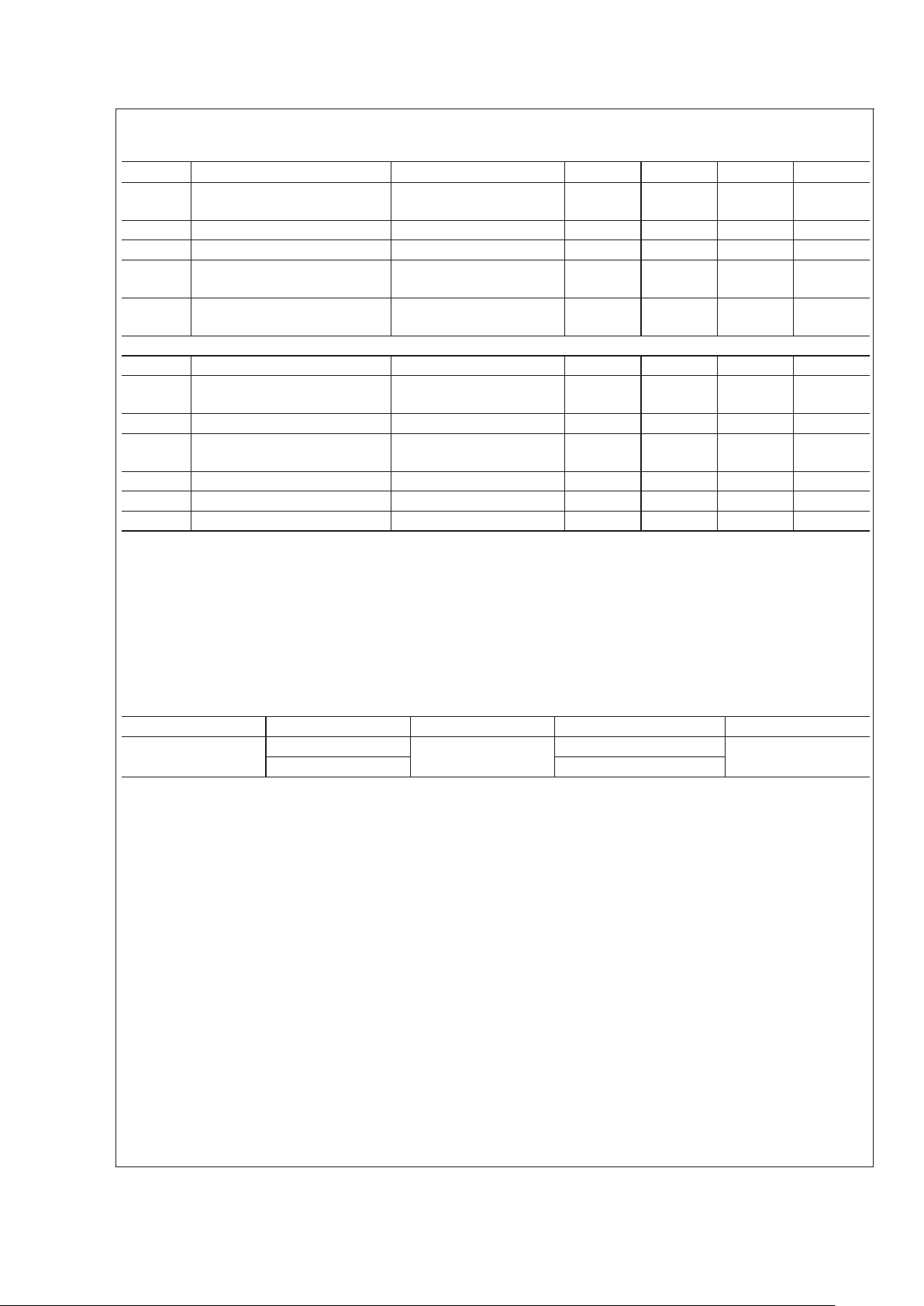
Typical Performance Characteristics (A
V
= +2, RL= 100Ω, Unless Specified).
Frequency Response vs. Gain Frequency Response
20040106
20040123
Frequency Response R
L
Frequency Response vs. R
L
20040125
20040124
Gain Flatness & Linear Phase Gain Flatness & Linear Phase
20040107
20040122
LMH6718
www.national.com5
 Loading...