

NSC LMH6683MT, LMH6683MAX, LMH6683MA, LMH6683MTX Datasheet
November 2002
LMH6682/6683
190MHz Single Supply, Dual and Triple Operational
Amplifiers
General Description
The LMH6682 and LMH6683 are high speed operational
amplifiers designed for use in modern video systems. These
single supply monolithic amplifiers extend National’s featurerich, high value video portfolio to include a dual and a triple
version. The important video specifications of differential
±
gain (
combined with an output drive current in each amplifier of
85mA make the LMH6682 and LMH6683 excellent choices
for a full range of video applications.
Voltage feedback topology in operational amplifiers assures
maximum flexibility and ease of use in high speed amplifier
designs. The LMH6682/83 is fabricated in National Semiconductor’s VIP10 process. This advanced process provides a
superior ratio of speed to quiescient current consumption
and assures the user of high-value amplifier designs. Advanced technology and circuit design enables in these amplifiers a −3db bandwidth of 190MHz, a slew rate of 940V/
µsec, and stability for gains of less than −1 and greater than
+2.
The input stage design of the LM6682/83 enables an input
signal range that extends below the negative rail. The output
stage voltage range reaches to within 0.8V of either rail
when driving a 2kΩ load. Other attractive features include
fast settling and low distortion. Other applications for these
amplifiers include servo control designs. These applications
are sensitive to amplifiers that exhibit phase reversal when
the inputs exceed the rated voltage range. The LMH6682/83
amplifiers are designed to be immune to phase reversal
when the specified input range is exceeded. See applications section. This feature makes for design simplicity and
flexibility in many industrial applications.
0.01% typ.) and differential phase (±0.08 degrees)
The LMH6682 dual operational amplifier is offered in miniature surface mount packages, SOIC-8, and MSOP-8. The
LMH6683 triple amplifier is offered in SOIC-14 and TSSOP-
14.
Features
VS=±5V, TA= 25˚C, RL= 100Ω, A = +2 (Typical values
unless specified)
n DG error 0.01%
n DP error 0.08˚
n −3dB BW (A = +2) 190MHz
n Slew rate (V
n Supply current 6.5mA/amp
n Output current +80/−90mA
n Input common mode voltage 0.5V beyond V
+
V
n Output voltage swing (RL=2kΩ) 0.8V from rails
n Input voltage noise (100KHz) 12nV/
=±5V) 940V/µs
S
Applications
n CD/DVD ROM
n ADC buffer amp
n Portable video
n Current sense buffer
n Portable communications
−
, 1.7V from
LMH6682/6683 190MHz Single Supply, Dual and Triple Operational Amplifiers
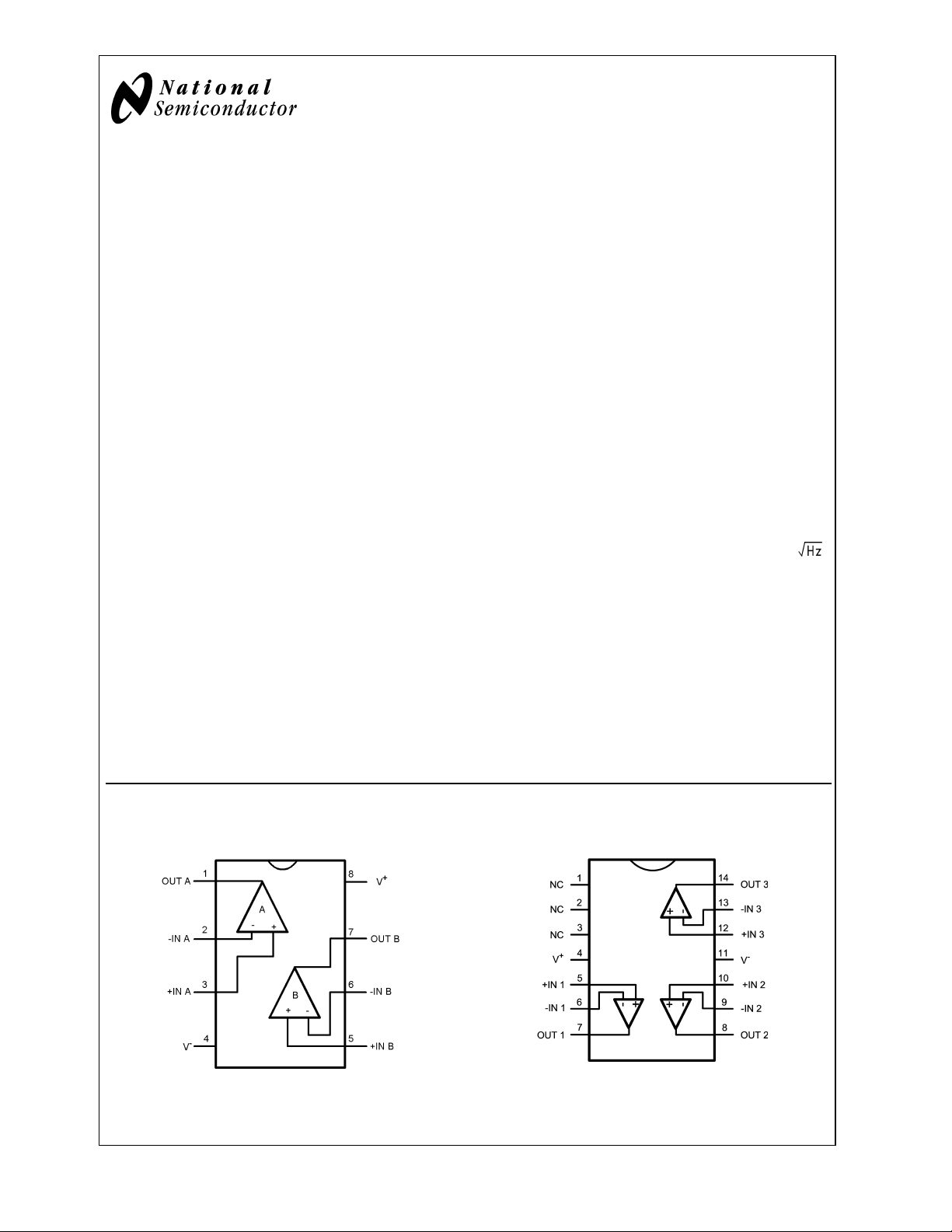
Connection Diagrams
SOIC-8/MSOP-8 (LMH6682) SOIC-14/TSSOP-14 (LMH6683)
Top View
20059002
© 2002 National Semiconductor Corporation DS200590 www.national.com
Top View
20059003
Absolute Maximum Ratings (Note 1)
If Military/Aerospace specified devices are required,
Storage Temperature Range −65˚C to +150˚C
Junction Temperature (Note 7) +150˚C
please contact the National Semiconductor Sales Office/
Distributors for availability and specifications.
LMH6682/6683
ESD Tolerance
Human Body Model 2KV(Note 2)
Machine Model 200V (Note 3)
Differential
V
IN
Output Short Circuit Duration (Note 4), (Note 6)
Input Current
Supply Voltage (V
Voltage at Input/Output pins V
+-V−
) 12.6V
+
+0.8V, V−−0.8V
Soldering Information
±
±
10mA
2.5V
Operating Ratings (Note 1)
Supply Voltage (V
Operating Temperature Range
(Note 7) −40˚C to +85˚C
Package Thermal Resistance (Note 7)
SOIC-8 190˚C/W
MSOP-8 235˚C/W
SOIC-14 145˚C/W
TSSOP-14 155˚C/W
+–V−
) 3Vto12V
Infrared or Convection (20 sec.) 235˚C
Wave Soldering (10 sec.) 260˚C
5V Electrical Characteristics
Unless otherwise specified, all limits guaranteed for at TJ= 25˚C, V+= 5V, V−= 0V, VO=VCM=V+/2, and RL= 100Ω to V+/2,
= 510Ω. Boldface limits apply at the temperature extremes.
R
F
Symbol Parameter Conditions Min
(Note 9)
SSBW −3dB BW A = +2, V
A = −1, V
GFP Gain Flatness Peaking A = +2, V
OUT
OUT
OUT
= 200mV
= 200mV
= 200mV
PP
PP
PP
DC to 100MHz
GFR Gain Flatness Rolloff A = +2, V
OUT
= 200mV
PP
DC to 100MHz
LPD 1˚ 1˚ Linear Phase Deviation A = +2, V
GF
0.1dB
0.1dB Gain Flatness A = +2,±0.1dB, V
FPBW Full Power −1dB Bandwidth A = +2, V
DG Differential Gain
NTSC 3.58MHz
DP Differential Phase
NTSC 3.58MHz
A = +2, R
Pos video only V
A = +2, R
Pos video only V
= 200mVPP,±1˚ 40 MHz
OUT
= 200mV
OUT
=2V
OUT
L
L
PP
= 150Ω to V+/2
=2V
CM
= 150Ω to V+/2
=2V
CM
PP
Time Domain Response
T
r/Tf
OS Overshoot A = +2, V
T
s
SR Slew Rate (Note 11) A = +2, V
Rise and Fall Time 20-80%, VO=1VPP,AV= +2 2.1
20-80%, V
=1VPP,AV=−1 2
O
= 100mV
O
PP
Settling Time VO=2VPP,±0.1%, AV=+2 49 ns
=3V
A = −1, V
OUT
OUT
=3V
PP
PP
Distortion and Noise Response
HD2 2
nd
Harmonic Distortion f = 5MHz, VO=2VPP, A = +2, RL=
2kΩ
f = 5MHz, V
=2VPP, A = +2, RL=
O
100Ω
HD3 3rdHarmonic Distortion f = 5MHz, VO=2VPP, A = +2, RL=
2kΩ
f = 5MHz, VO=2VPP, A = +2, RL=
100Ω
140 180
Typ
(Note 8)
Max
(Note 9)
180
2.1 dB
0.1 dB
25 MHz
110 MHz
0.03 %
0.05 deg
22 %
520
500
−60
−61
−77
−54
Units
MHz
ns
V/µs
dBc
dBc
www.national.com 2
5V Electrical Characteristics (Continued)
Unless otherwise specified, all limits guaranteed for at TJ= 25˚C, V+= 5V, V−= 0V, VO=VCM=V+/2, and RL= 100Ω to V+/2,
= 510Ω. Boldface limits apply at the temperature extremes.
R
F
Symbol Parameter Conditions Min
(Note 9)
Distortion and Noise Response
THD Total Harmonic Distortion f = 5MHz, V
=2VPP, A = +2, RL=
O
2kΩ
f = 5MHz, VO=2VPP, A = +2, RL=
100Ω
e
n
Input Referred Voltage Noise f = 1kHz 17 nV/
f = 100kHz 12
i
n
Input Referred Current Noise f = 1kHz 8 pA/
f = 100kHz 3
CT Cross-Talk Rejection
(Amplifier)
f = 5MHz, A = +2, SND: R
F=RG
= 510Ω
RCV: R
= 100Ω
L
Static, DC Performance
A
VOL
CMVR Input Common-Mode Voltage
Large Signal Voltage Gain VO= 1.25V to 3.75V,
=2kΩ to V+/2
R
L
V
= 1.5V to 3.5V,
O
= 150Ω to V+/2
R
L
V
=2Vto3V,
O
=50Ω to V+/2
R
L
CMRR ≥ 50dB −0.2
Range
V
OS
TC V
Input Offset Voltage
Input Offset Voltage Average
OS
(Note 12)
Drift
I
B
TC
IB
I
OS
CMRR Common Mode Rejection
Input Bias Current (Note 10) −5 −20
Input Bias Current Drift 0.01 nA/˚C
Input Offset Current 50 300
Stepped from 0V to 3.0V 72 82 dB
V
CM
Ratio
+
+PSRR Positive Power Supply
= 4.5V to 5.5V, VCM=1V 70 76 dB
V
Rejection Ratio
I
S
Supply Current (per channel) No load 6.5 9
85 95
75 85
70 80
−0.1
3.0
2.8
Typ
(Note 8)
Max
(Note 9)
−60
−53
−77 dB
−0.5
3.3
±
1.1
±
2 µV/˚C
±
5
±
7
−30
500
11
Units
dBc
mV
mA
LMH6682/6683
dB
V
µA
nA
www.national.com3
5V Electrical Characteristics (Continued)
Unless otherwise specified, all limits guaranteed for at TJ= 25˚C, V+= 5V, V−= 0V, VO=VCM=V+/2, and RL= 100Ω to V+/2,
= 510Ω. Boldface limits apply at the temperature extremes.
R
F
Symbol Parameter Conditions Min
LMH6682/6683
Miscellaneous Performance
V
I
I
R
C
R
O
OUT
SC
IN
IN
OUT
Output Swing
RL=2kΩ to V+/2 4.10
High
RL= 150Ω to V+/2 3.90
=75Ω to V+/2 3.75
R
L
Output Swing
RL=2kΩ to V+/2 800 920
Low
= 150Ω to V+/2 870 970
R
L
RL=75Ω to V+/2 885 1100
Output Current VO= 1V from either supply rail
Output Short Circuit Current
Sourcing to V+/2 −100
(Note 5), (Note 6), (Note 10)
+
Sinking from V
/2 100
Common Mode Input
Resistance
Common Mode Input
Capacitance
Output Resistance Closed
Loop
f = 1kHz, A = +2, RL=50Ω 0.02
f = 1MHz, A = +2, R
=50Ω 0.12
L
(Note 9)
3.8
3.70
3.50
±
40 +80/−75 mA
−80
80
Typ
(Note 8)
4.25
4.19
4.15
−155
220
3
1.6
Max
(Note 9)
1100
1200
1250
Units
V
mV
mA
MΩ
pF
Ω
±
5V Electrical Characteristics
Unless otherwise specified, all limits guaranteed for at TJ= 25˚C, V+= 5V, V−= −5V, VO=VCM= 0V, and RL= 100Ω to 0V,
= 510Ω. Boldface limits apply at the temperature extremes.
R
F
Symbol Parameter Conditions Min
(Note 9)
SSBW −3dB BW A = +2, V
A = −1, V
GFP Gain Flatness Peaking A = +2, V
OUT
OUT
OUT
= 200mV
= 200mV
= 200mV
PP
PP
PP
150 190
Typ
(Note 8)
Max
(Note 9)
190
1.7 dB
DC to 100MHz
GFR Gain Flatness Rolloff A = +2, V
OUT
= 200mV
PP
0.1 dB
DC to 100MHz
LPD 1˚ 1˚ Linear Phase Deviation A = +2, V
GF
0.1dB
0.1dB Gain Flatness A = +2,±0.1dB, V
FPBW Full Power −1dB Bandwidth A = +2, V
DG Differential Gain
A = +2, R
= 200mVPP,±1˚ 40 MHz
OUT
= 200mV
OUT
=2V
OUT
L
PP
= 150Ω to 0V 0.01 %
PP
25 MHz
120 MHz
NTSC 3.58MHz
DP Differential Phase
A = +2, RL= 150Ω to 0V 0.08 deg
NTSC 3.58MHz
Time Domain Response
T
r/Tf
OS Overshoot A = +2, V
T
s
Rise and Fall Time 20-80%, VO=1VPP,A=+2 1.9
20-80%, V
=1VPP,A=−1 2
O
= 100mV
O
PP
19 %
Settling Time VO=2VPP,±0.1%, A = +2 42 ns
Units
MHz
ns
www.national.com 4
±
5V Electrical Characteristics (Continued)
Unless otherwise specified, all limits guaranteed for at TJ= 25˚C, V+= 5V, V−= −5V, VO=VCM= 0V, and RL= 100Ω to 0V,
= 510Ω. Boldface limits apply at the temperature extremes.
R
F
Symbol Parameter Conditions Min
(Note 9)
Typ
(Note 8)
Max
(Note 9)
Time Domain Response
SR Slew Rate (Note 11) A = +2, V
A = −1, V
OUT
OUT
=6V
=6V
PP
PP
940
900
Distortion and Noise Response
HD2 2
nd
Harmonic Distortion f = 5MHz, VO=2VPP, A = +2, RL=
−63
2kΩ
f = 5MHz, V
=2VPP, A = +2, RL=
O
−66
100Ω
HD3 3rdHarmonic Distortion f = 5MHz, VO=2VPP, A = +2, RL=
−82
2kΩ
f = 5MHz, VO=2VPP, A = +2, RL=
−54
100Ω
THD Total Harmonic Distortion f = 5MHz, V
=2VPP, A = +2, RL=
O
−63
2kΩ
f = 5MHz, V
=2VPP, A = +2, RL=
O
−54
100Ω
e
n
Input Referred Voltage Noise f = 1kHz 18 nV/
f = 100kHz 12
i
n
Input Referred Current Noise f = 1kHz 6 pA/
f = 100kHz 3
CT Cross-Talk Rejection
(Amplifier)
f = 5MHz, A = +2, SND: R
F=RG
= 510Ω
RCV: R
= 100Ω
L
−78 dB
Static, DC Performance
A
VOL
Large Signal Voltage Gain VO= −3.75V to 3.75V,
CMVR Input Common Mode Voltage
Range
=2kΩ to V+/2
R
L
V
= −3.5V to 3.5V,
O
= 150Ω to V+/2
R
L
V
= −3V to 3V,
O
=50Ω to V+/2
R
L
CMRR ≥ 50dB −5.2
87 100
80 90
75 85
−5.1
3.0
−5.5
3.3
2.8
V
OS
TC V
Input Offset Voltage
Input Offset Voltage Average
OS
(Note 12)
±
1
±
2 µV/˚C
±
5
±
7
Drift
I
B
Input Bias Current (Note 10) −5 −20
−30
TC
I
OS
IB
Input Bias Current Drift 0.01 nA/˚C
Input Offset Current 50 300
500
CMRR Common Mode Rejection
Stepped from −5V to 3.0V 75 84 dB
V
CM
Ratio
+PSRR Positive Power Supply
Rejection Ratio
−PSRR Negative Power Supply
Rejection Ratio
V+= 8.5V to 9.5V,
−
= −1V
V
−
V
= −4.5V to −5.5V,
+
=5V
V
75 82 dB
78 85 dB
LMH6682/6683
Units
V/µs
dBc
dBc
dBc
dB
V
mV
µA
nA
www.national.com5
±
5V Electrical Characteristics (Continued)
Unless otherwise specified, all limits guaranteed for at TJ= 25˚C, V+= 5V, V−= −5V, VO=VCM= 0V, and RL= 100Ω to 0V,
= 510Ω. Boldface limits apply at the temperature extremes.
R
F
Symbol Parameter Conditions Min
LMH6682/6683
(Note 9)
Typ
(Note 8)
Max
(Note 9)
Static, DC Performance
I
S
Supply Current (per channel) No load 6.5 9.5
11
Miscellaneous Performance
V
O
Output Swing
High
RL=2kΩ to 0V 4.10
3.80
= 150Ω to 0V 3.90
R
L
4.25
4.20
3.70
RL=75Ω to 0V 3.75
4.18
3.50
Output Swing
Low
=2kΩ to 0V −4.19 −4.07
R
L
= 150Ω to 0V −4.05 −3.89
R
L
−3.80
−3.65
RL=75Ω to 0V −4.00 −3.70
−3.50
I
I
OUT
SC
Output Current VO= 1V from either supply rail
Output Short Circuit Current
Sourcing to 0V −120
(Note 5) , (Note 6),(Note 10)
Sinking from 0V 120
±
45 +85/−80 mA
−180
−100
230
100
R
IN
Common Mode Input
4
Resistance
C
IN
Common Mode Input
1.6
Capacitance
R
OUT
Note 1: Absolute maximum Ratings indicate limits beyond which damage to the device may occur. Operating Ratings indicate conditions for which the device is
intended to be functional, but specific performance is not guaranteed. For guaranteed specifications and the test conditions, see the Electrical Characteristics.
Note 2: Human body model, 1.5kΩ in series with 100pF.
Note 3: Machine Model, 0Ω in series with 200pF.
Note 4: Applies to both single-supply and split-supply operation. Continuous short circuit operation at elevated ambient temperature can result in exceeding the
maximum allowed junction temperature of 150˚C.
Note 5: Short circuit test is a momentary test. See next note.
Note 6: Output short circuit duration is infinite for V
Note 7: The maximum power dissipation is a function of T
P
D
Note 8: Typical values represent the most likely parametric norm.
Note 9: All limits are guaranteed by testing or statistical analysis.
Note 10: Positive current corresponds to current flowing into the device.
Note 11: Slew rate is the average of the rising and falling slew rates
Note 12: Offset Voltage average drift determined by dividing the change in V
Output Resistance Closed
Loop
=(T
J(MAX)-TA
)/ θJA. All numbers apply for packages soldered directly onto a PC board.
f = 1kHz, A = +2, RL=50Ω 0.02
f = 1MHz, A = +2, R
<
6V at room temperature and below. For V
S
, θJA, and TA. The maximum allowable power dissipation at any ambient temperature is
J(MAX)
=50Ω 0.12
L
>
6V, allowable short circuit duration is 1.5ms.
S
at temperature extremes into the total temperature change.
OS
Units
mA
V
mV
mA
MΩ
pF
Ω
www.national.com 6
 Loading...