

NSC LMH6647MAX, LMH6647MA, LMH6645MF, LMH6645MA, LMH6645MFX Datasheet
LMH6645/46/47
2.7V, 650µA, 55MHz, Rail-to-Rail Input and Output
Amplifiers with Shutdown Option
February 2002
LMH6645/46/47 2.7V, 650µA, 55MHz, Rail-to-Rail Input and Output Amplifiers with Shutdown
Option
General Description
The LMH6645 (single) and LMH6646 (dual), rail-to-rail input
and output voltage feedback amplifiers, offer high speed
(55MHz), and low voltage operation (2.7V) in addition to
micro-power shutdown capability (LMH6647, single).
Input common modevoltage range exceeds either supply by
0.3V, enhancing ease of use in multitude of applications
where previously only inferior devices could be used. Output
voltage range extends to within 20mV of either supply rails,
allowing wide dynamic range especially in low voltage applications. Even with low supply current of 650µA/amplifier,
output current capability is kept at a respectable
driving heavier loads. Important device parameters such as
BW, Slew Rate and output current are kept relatively independent of the operating supply voltage by a combination of
process enhancements and design architecture.
In portable applications, the LMH6647 provides shutdown
capability while keeping the turn-off current to less than
50µA. Both turn-on and turn-off characteristics are well behaved with minimal output fluctuations during transitions.
This allows the part to be used in power saving mode, as
well as multiplexing applications. Miniature packages
(SOT23, MSOP-8, and SO-8) are further means to ease the
adoption of these low power high speed devices in applications where board area is at a premium.
±
20mA for
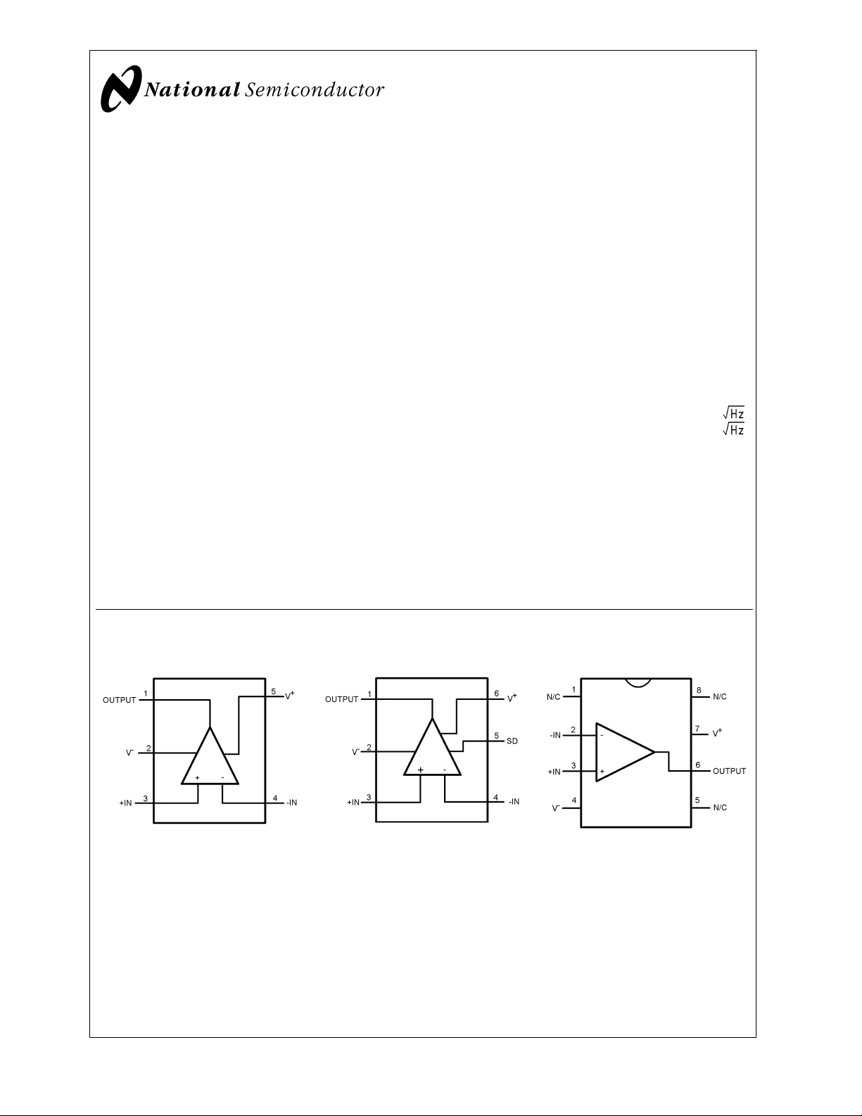
Connection Diagrams
Features
(VS= 2.7V, TA= 25˚C, RL=1kΩto V+/2, AV= +1. Typical
values unless specified).
n −3dB BW 55MHz
n Supply voltage range 2.5V to 12V
n Slew rate 22V/µs
n Supply current 650µA/channel
n Output short circuit current 42mA
n Linear output current
n Input common mode voltage 0.3V beyond rails
n Output voltage swing 20mV from rails
n Input voltage noise 17nV/
n Input current noise 0.75pA/
±
20mA
Applications
n Active filters
n High speed portable devices
n Multiplexing applications (LMH6647)
n Current sense buffer
n High speed transducer amp
SOT23-5 (LMH6645) SOT23-6 (LMH6647) SOIC-8 (LMH6645)
Top View
20020259
© 2002 National Semiconductor Corporation DS200202 www.national.com
Top View
20020260
Top View
20020261
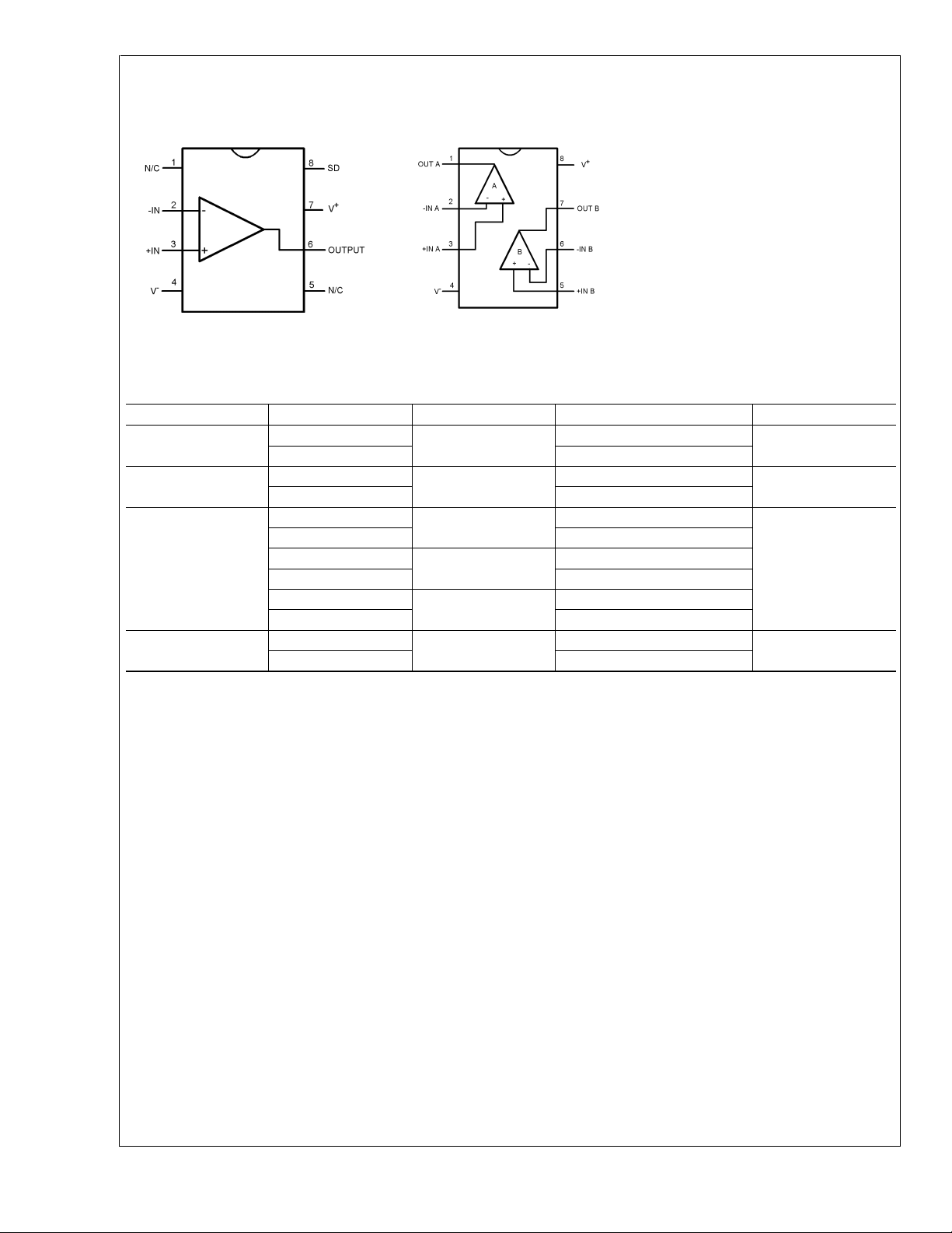
Connection Diagrams (Continued)
SOIC-8 (LMH6647)
LMH6645/46/47
SOIC-8 and MSOP-8
(LMH6646)
20020263
Top View
20020262
Top View
Ordering Information
Package Part Number Package Marking Transport Media NSC Drawing
5-Pin SOT-23 LMH6645MF A68A 1k Units Tape and Reel MF05A
LMH6645MFX 3k Units Tape and Reel
6-Pin SOT-23 LMH6647MF A69A 1k Units Tape and Reel MF06A
LMH6647MFX 3k Units Tape and Reel
SOIC-8 LMH6645MA LMH6645MA 95 Units Rails M08A
LMH6645MAX 2.5k Units Tape and Reel
LMH6646MA LMH6646MA 95 Units Rails
LMH6646MAX 2.5k Units Tape and Reel
LMH6647MA LMH6647MA 95 Units Rails
LMH6647MAX 2.5k Units Tape and Reel
MSOP-8 LMH6646MM A70A 1k Units Tape and Reel MUA08A
LMH6646MMX 3.5k Units Tape and Reel
www.national.com 2
LMH6645/46/47
Absolute Maximum Ratings (Note 1)
If Military/Aerospace specified devices are required,
please contact the National Semiconductor Sales Office/
Distributors for availability and specifications.
ESD Tolerance
Human Body 2KV (Note 2)
Machine Model 200V (Note 9)
V
Differential
IN
Output Short Circuit Duration (Note 3, 11)
Supply Voltage (V
Voltage at Input/Output pins V
+-V−
) 12.6V
+
+0.8V, V−−0.8V
Storage Temperature Range −65˚C to +150˚C
Junction Temperature (Note 4) +150˚C
±
2.5V
Soldering Information
Infrared or Convection (20 sec) 235˚C
Wave Soldering (10 sec) 260˚C
Operating Ratings (Note 1)
Supply Voltage (V
Junction Temperature Range (Note 4) −40˚C to +85˚C
Package Thermal Resistance (Note 4) (θ
SOT23-5 265˚C/W
SOT23-6 265˚C/W
SOIC-8 190˚C/W
MSOP-8 235˚C/W
+–V−
) 2.5V to 12V
)
JA
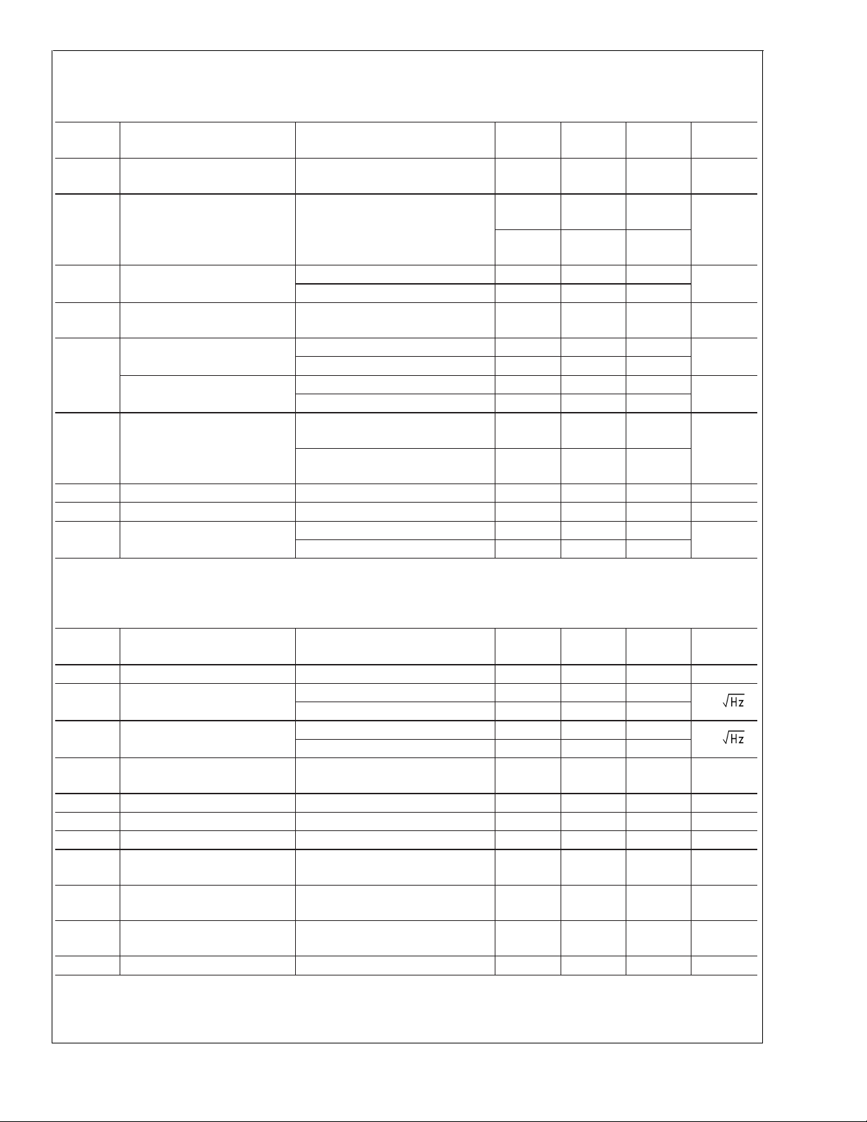
2.7V Electrical Characteristics
Unless otherwise specified, all limits guaranteed for at TJ= 25˚C, V+= 2.7V, V−= 0V, VCM=VO=V+/2, and Rf=2kΩ, and R
=1kΩto V+/2. Boldface limits apply at the temperature extremes.
Symbol Parameter Conditions Min
(Note 6)
BW −3dB BW A
e
n
Input-Referred Voltage Noise f = 100kHz 17
V
V
CM
= +1, V
= 0.7V
= 200mVPP,
OUT
f = 1kHz 25
i
n
Input-Referred Current Noise f = 100kHz 0.75
f = 1kHz 1.20
CT Rej. Cross-Talk Rejection
(LMH6646 only)
SR Slew Rate A
f = 5MHz, Receiver:
R
= 510Ω,AV=+2
f=Rg
= −1, VO=2V
V
PP
(Note 8, 13)
T
ON
Turn-On Time
(LMH6647 only)
T
OFF
Turn-Off Time
(LMH6647 only)
TH
SD
Shutdown Threshold
IS≤ 50µA 1.95 2.30
(LMH6647 only)
I
SD
Shutdown Pin Input Current
(Note 7) −20 µA
(LMH6647 only)
V
OS
TC V
I
B
I
OS
R
IN
Input Offset Voltage 0V ≤ VCM≤ 2.7V −3
Input Offset Average Drift (Note 12)
OS
Input Bias Current VCM= 2.5V (Note 7) 0.40 2
= 0.5V (Note 7) −0.68 −2
V
CM
Input Offset Current 0V ≤ VCM≤ 2.7V 1 500 nA
Common Mode Input
Resistance
C
IN
Common Mode Input
Capacitance
CMVR Input Common-Mode Voltage
CMRR ≥ 50dB −0.5 −0.3
Range
40 55 MHz
15 22 V/µs
−4
3.0
2.8
Typ
(Note 5)
Max
(Note 6)
Units
nV/
pA/
47 dB
250 ns
560 ns
±
13
4
±
5 µV/˚C
2.2
−2.2
3MΩ
2pF
−0.1
3.2
L
V
mV
µA
V
www.national.com3
2.7V Electrical Characteristics (Continued)
Unless otherwise specified, all limits guaranteed for at TJ= 25˚C, V+= 2.7V, V−= 0V, VCM=VO=V+/2, and Rf=2kΩ, and R
=1kΩto V+/2. Boldface limits apply at the temperature extremes.
Symbol Parameter Conditions Min
LMH6645/46/47
CMRR Common Mode Rejection
Ratio
A
VOL
V
O
Large Signal Voltage Gain VO= 0.35V to 2.35V 76
Output Swing
High
Output Swing
Low
I
I
SC
OUT
Output Short Circuit Current Sourcing to V
Output Current V
PSRR Power Supply Rejection Ratio V
I
S
Supply Current (per channel) Normal Operation 650 1250
V
Stepped from 0V to 2.7V 46 77
CM
Stepped from 0V to 1.55V 58 76
V
CM
RL=1ktoV+/2 2.55 2.66
= 10k to V+/2 2.68
R
L
R
=1ktoV+/2 40 150
L
= 10k to V+/2 20
R
L
−
VID= 200mV (Note 10)
Sinking to V
+
VID= −200mV (Note 10)
= 0.5V from rails
OUT
+
= 2.7V to 3.7V or
−
=0Vto−1V
V
Shutdown Mode (LMH6647 only) 15 50
(Note 6)
74
75 83 dB
Typ
(Note 5)
Max
(Note 6)
87 dB
43
42
±
20 mA
L
Units
dB
V
mV
mA
µA
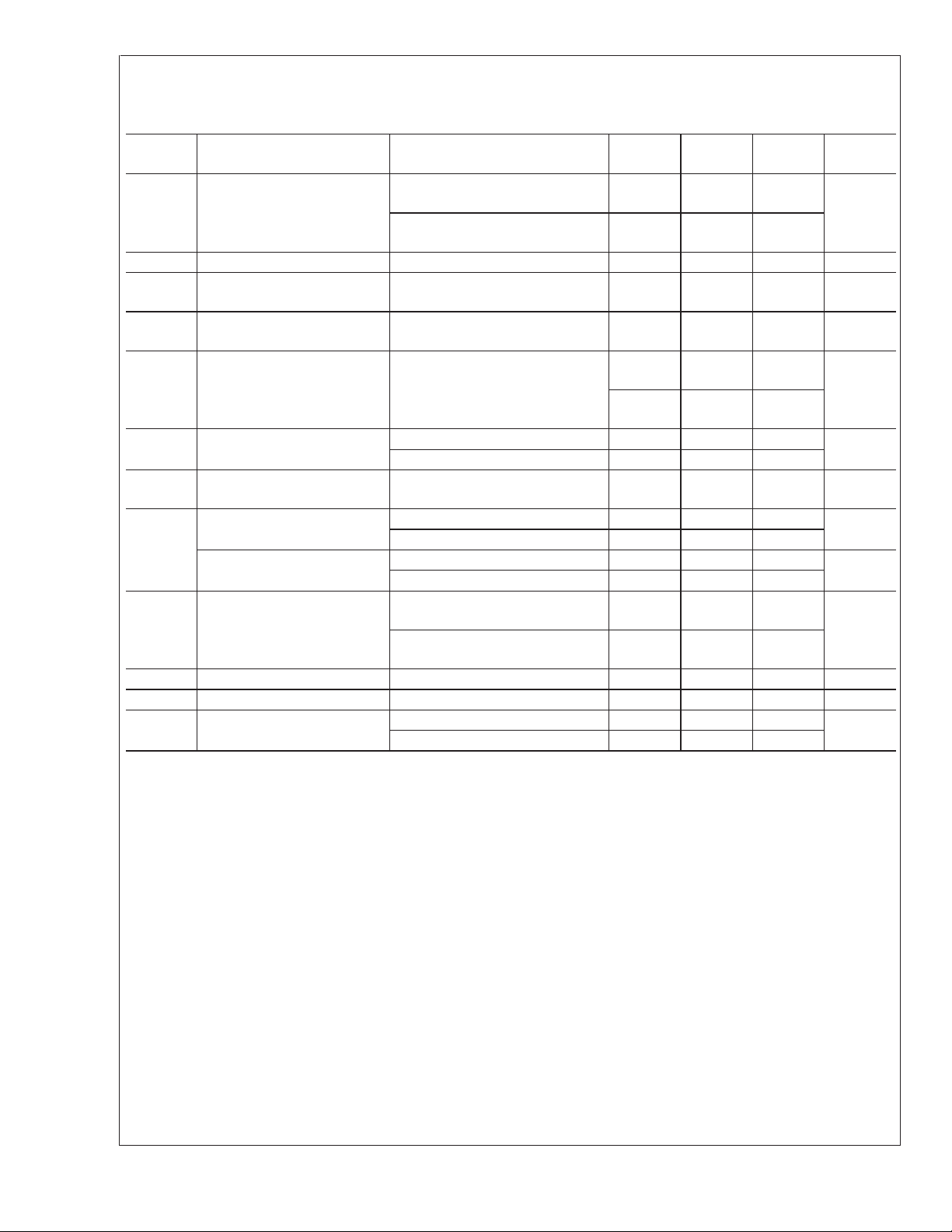
5V Electrical Characteristics
Unless otherwise specified, all limits guaranteed for at TJ= 25˚C, V+= 5V, V−= 0V, VCM=VO=V+/2, and Rf=2kΩ, and R
=1kΩto V+/2. Boldface limits apply at the temperature extremes.
Symbol Parameter Conditions Min
(Note 6)
BW −3dB BW A
e
n
Input-Referred Voltage Noise f = 100kHz 17
= +1, V
V
OUT
= 200mV
PP
f = 1kHz 25
i
n
Input-Referred Current Noise f = 100kHz 0.75
f = 1kHz 1.20
CT Rej. Cross-Talk Rejection
(LMH6646 only)
SR Slew Rate A
f = 5MHz, Receiver:
R
= 510Ω,AV=+2
f=Rg
= −1, VO=2V
V
PP
(Note 8, 13)
T
T
TH
ON
OFF
SD
Turn-On Time (LMH6647 only) 210 ns
Turn-Off Time (LMH6647 only) 500 ns
Shutdown Threshold
IS≤ 50µA 4.25 4.60 V
(LMH6647 only)
I
SD
Shutdown Pin Input Current
(Note 7)
(LMH6647 only)
V
OS
TC V
I
B
I
OS
R
IN
Input Offset Voltage 0V ≤ VCM≤ 5V −3
Input Offset Average Drift (Note 12)
OS
Input Bias Current VCM= 4.8V (Note 7)
= 0.5V (Note 7)
V
CM
Input Offset Current 0V ≤ VCM≤ 5V 1 500 nA
Common Mode Input
Resistance
40 55 MHz
15 22
−4
Typ
(Note 5)
Max
(Note 6)
nV/
pA/
47 dB
−20 µA
±
1
±
5 µV/C
+0.36
−0.68
3
4
+2
−2.2
−2
−2.2
3MΩ
L
Units
V/µs
mV
µA
www.national.com 4
5V Electrical Characteristics (Continued)
Unless otherwise specified, all limits guaranteed for at TJ= 25˚C, V+= 5V, V−= 0V, VCM=VO=V+/2, and Rf=2kΩ, and R
=1kΩto V+/2. Boldface limits apply at the temperature extremes.
Symbol Parameter Conditions Min
(Note 6)
C
IN
Common Mode Input
Capacitance
CMVR Input Common-Mode Voltage
CMRR ≥ 50dB −0.5 −0.3
Range
CMRR Common Mode Rejection
Ratio
A
VOL
V
O
Large Signal Voltage Gain VO= 1.5V to 3.5V 76
Output Swing
High
Output Swing
Low
I
SC
Output Short Circuit Current Sourcing to V
Stepped from 0V to 5V 56 82
V
CM
Stepped from 0V to 3.8V 66 85
V
CM
RL=1ktoV+/2 4.80 4.95
= 10k to V+/2 4.98
R
L
R
=1ktoV+/2 50 200
L
= 10k to V+/2 20
R
L
−
VID= 200mV (Note 10)
Sinking to V
+
VID= −200mV (Note 10)
I
OUT
Output Current V
PSRR Power Supply Rejection Ratio V
I
S
Supply Current (per channel) Normal Operation 700 1400
= 0.5V From rails
OUT
+
=5Vto6VorV−= 0V to −1V 75 95 dB
Shutdown Mode (LMH6647 only) 10 50
5.3
5.1
74
Typ
(Note 5)
Max
(Note 6)
2pF
−0.1
5.5
85
55
53
±
20 mA
LMH6645/46/47
L
Units
V
dB
dB
V
mV
mA
µA
±
5V Electrical Characteristics
Unless otherwise specified, all limits guaranteed for at TJ= 25˚C, V+= 5V, V−= −5V, VCM=VO= 0V, Rf=2kΩ, and RL=
1kΩ to GND. Boldface limits apply at the temperature extremes.
Symbol Parameter Conditions Min
(Note 6)
BW −3dB BW A
e
n
Input-Referred Voltage Noise f = 100kHz 17
= +1, V
V
OUT
= 200mV
PP
40 55 MHz
Typ
(Note 5)
Max
(Note 6)
f = 1kHz 25
i
n
Input-Referred Current Noise f = 100kHz 0.75
f = 1kHz 1.20
CT Rej. Cross-Talk Rejection
(LMH6646 only)
SR Slew Rate A
T
T
TH
ON
OFF
SD
Turn-On Time (LMH6647 only) 200 ns
Turn-Off Time (LMH6647 only) 700 ns
Shutdown Threshold
(LMH6647 only)
I
SD
Shutdown Pin Input Current
f = 5MHz, Receiver:
R
= 510Ω,AV=+2
f=Rg
= −1, VO=2VPP(Note 8) 15 22 V/µs
V
IS≤ 50µA
47 dB
4.25 4.60
(Note 7) −20 µA
(LMH6647 only)
V
OS
TC V
Input Offset Voltage −5V ≤ VCM≤ 5V −3
Input Offset Average Drift (Note 12)
OS
−4
±
1
±
5 µV/˚C
3
4
Units
nV/
pA/
V
mV
www.national.com5
±
5V Electrical Characteristics (Continued)
Unless otherwise specified, all limits guaranteed for at TJ= 25˚C, V+= 5V, V−= −5V, VCM=VO= 0V, Rf=2kΩ, and RL=
1kΩ to GND. Boldface limits apply at the temperature extremes.
Symbol Parameter Conditions Min
LMH6645/46/47
I
B
I
OS
R
IN
Input Bias Current VCM= 4.8V (Note 7)
= −4.5V (Note 7)
V
CM
Input Offset Current −5V ≤ VCM≤ 5V 3 500 nA
Common Mode Input
(Note 6)
Typ
(Note 5)
+0.40
−0.65
Max
(Note 6)
+2
+2.2
−2
−2.2
3MΩ
Resistance
C
IN
Common Mode Input
2pF
Capacitance
CMVR Input Common-Mode Voltage
Range
CMRR ≥ 50dB −5.5 −5.3
−5.1
5.3
5.5
5.1
CMRR Common Mode Rejection
Ratio
A
VOL
Large Signal Voltage Gain VO= −2V to 2V 76
Stepped from −5V to 5V 60 84
V
CM
Stepped from −5V to 3.5V 66 104
V
CM
85
74
V
O
I
SC
I
OUT
PSRR Power Supply Rejection Ratio V
I
S
Output Swing
High
Output Swing
Low
Output Short Circuit Current Sourcing to V
Output Current V
RL=1kΩ 4.70 4.92
= 10kΩ 4.97
R
L
R
=1kΩ −4.93 −4.70
L
= 10kΩ −4.98
R
L
VID= 200mV (Note 10)
Sinking to V
VID= −200mV (Note 10)
OUT
+
=5Vto6VorV−= −5V to −6V 76 95 dB
−
+
= 0.5V from rails
66
61
±
20 mA
Supply Current (per channel) Normal Operation 725 1600
Shutdown Mode (LMH6647 only) 10 50
Note 1: Absolute Maximum Ratings indicate limits beyond which damage to the device may occur. Operating Ratings indicate conditions for which the device is
intended to be functional, but specific performance is not guaranteed. For guaranteed specifications and the test conditions, see the Electrical Characteristics.
Note 2: Human body model, 1.5kΩ in series with 100pF.
Note 3: Applies to both single-supply and split-supply operation. Continuous short circuit operation at elevated ambient temperature can result in exceeding the
maximum allowed junction temperature of 150˚C.
Note 4: The maximum power dissipation is a function of T
=(T
P
D
J(MAX)-TA
Note 5: Typical values represent the most likely parametric norm.
Note 6: All limits are guaranteed by testing or statistical analysis.
Note 7: Positive current corresponds to current flowing into the device.
Note 8: Slew rate is the average of the rising and falling slew rates.
Note 9: Machine Model, 0Ω in series with 200pF.
Note 10: Short circuit test is a momentary test. See Note 11.
Note 11: Output short circuit duration is infinite for V
Note 12: Offset voltage average drift determined by dividing the change in V
Note 13: Guaranteed based on characterization only.
)/ θJA. All numbers apply for packages soldered directly onto a PC board.
<
6V at room temperature and below. For V
S
, θJA, and TA. The maximum allowable power dissipation at any ambient temperature is
J(MAX)
>
6V, allowable short circuit duration is 1.5ms.
at temperature extremes into the total temperature change.
OS
S
Units
µA
V
dB
dB
V
V
mA
µA
www.national.com 6
 Loading...