

NSC LMH6644MTX, LMH6644MT, LMH6644MAX, LMH6643MWC, LMH6643MDC Datasheet
...
LMH6642/6643/6644
3V, Low Power, 130MHz, 75mA Rail-to-Rail Output
Amplifiers
General Description
The LMH664X family true single supply voltage feedback
amplifiers offer high speed (130MHz), low distortion
(−62dBc), and exceptionally high output current (approximately 75mA) at low cost and with reduced power consumption when compared against existing devices with similar
performance.
Input common mode voltage range extends to 0.5V below V
−
and 1V from V+. Output voltage range extends to within
40mV of either supply rail, allowing wide dynamic range
especially desirable in low voltage applications. The output
stage is capable of approximately 75mA in order to drive
heavy loads. Fast output Slew Rate (130V/µs) ensures large
peak-to-peak output swings can be maintained even at
higher speeds, resulting in exceptional full power bandwidth
of 40MHz with a 3V supply. These characteristics, along with
low cost, are ideal features for a multitude of industrial and
commercial applications.
Careful attention has been paid to ensure device stability
under all operating voltages and modes. The result is a very
well behaved frequency response characteristic (0.1dB gain
flatness up the 12MHz under 150Ω load and A
V
= +2) with
minimal peaking (typically 2dB maximum) for any gain setting and under both heavy and light loads. This along with
fast settling time (68ns) and low distortion allows the device
to operate well in ADC buffer, and high frequency filter
applications as well as other applications.
This device family offers professional quality video performance with low DG (0.01%) and DP (0.01˚) characteristics.
Differential Gain and Differential Phase characteristics are
also well maintained under heavy loads (150Ω) and throughout the output voltage range. The LMH664X family is offered
in single (LMH6642), dual (LMH6643), and quad (LMH6644)
options. See ordering information for packages offered.
Features
(VS=±5V, TA= 25˚C, RL=2kΩ,AV= +1. Typical values
unless specified).
n −3dB BW (A
V
= +1) 130MHz
n Supply voltage range 3V to 12.8V
n Slew rate (Note 8), (A
V
= −1) 130V/µs
n Supply current (no load) 2.7mA/amp
n Output short circuit current +115mA/−145mA
n Linear output current
±
75mA
n Input common mode volt. 0.5V beyond V
−
, 1V from V
+
n Output voltage swing 40mV from rails
n Input voltage noise (100kHz) 17nV/
n Input current noise (100kHz) 0.9pA/
n THD (5MHz, RL=2kΩ,VO=2VPP,AV= +2) −62dBc
n Settling time 68ns
n Fully characterized for 3V, 5V, and
±
5V
n Overdrive recovery 100ns
n Output short circuit protected (Note 11)
n No output phase reversal with CMVR exceeded
Applications
n Active filters
n CD/DVD ROM
n ADC buffer amp
n Portable video
n Current sense buffer
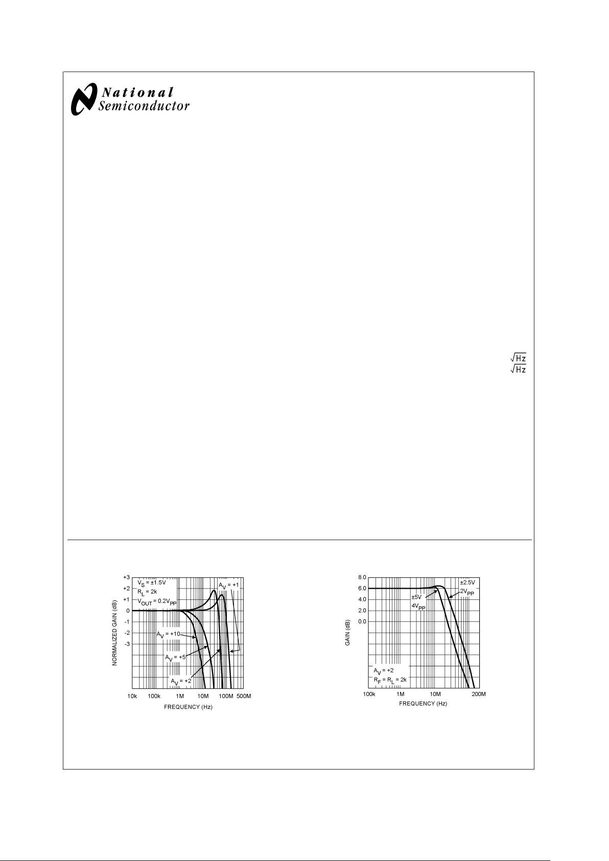
Closed Loop Gain vs. Frequency for Various Gain Large Signal Frequency Response
20018535
20018547
May 2003
LMH6642/6643/6644 3V, Low Power, 130MHz, 75mA Rail-to-Rail Output Amplifiers
© 2003 National Semiconductor Corporation DS200185 www.national.com
Absolute Maximum Ratings (Note 1)
If Military/Aerospace specified devices are required,
please contact the National Semiconductor Sales Office/
Distributors for availability and specifications.
ESD Tolerance 2KV (Note 2)
200V (Note 9)
V
IN
Differential
±
2.5V
Output Short Circuit Duration (Note 3), (Note 11)
Supply Voltage (V
+-V−
) 13.5V
Voltage at Input/Output pins V
+
+0.8V, V−−0.8V
Input Current
±
10mA
Storage Temperature Range −65˚C to +150˚C
Junction Temperature (Note 4) +150˚C
Soldering Information
Infrared or Convection Reflow(20 sec) 235˚C
Wave Soldering Lead Temp.(10 sec) 260˚C
Operating Ratings (Note 1)
Supply Voltage (V
+–V−
) 3V to 12.8V
Junction Temperature Range (Note 4) −40˚C to +85˚C
Package Thermal Resistance (Note 4) (θ
JA
)
SOT23-5 265˚C/W
SOIC-8 190˚C/W
MSOP-8 235˚C/W
SOIC-14 145˚C/W
TSSOP-14 155˚C/W
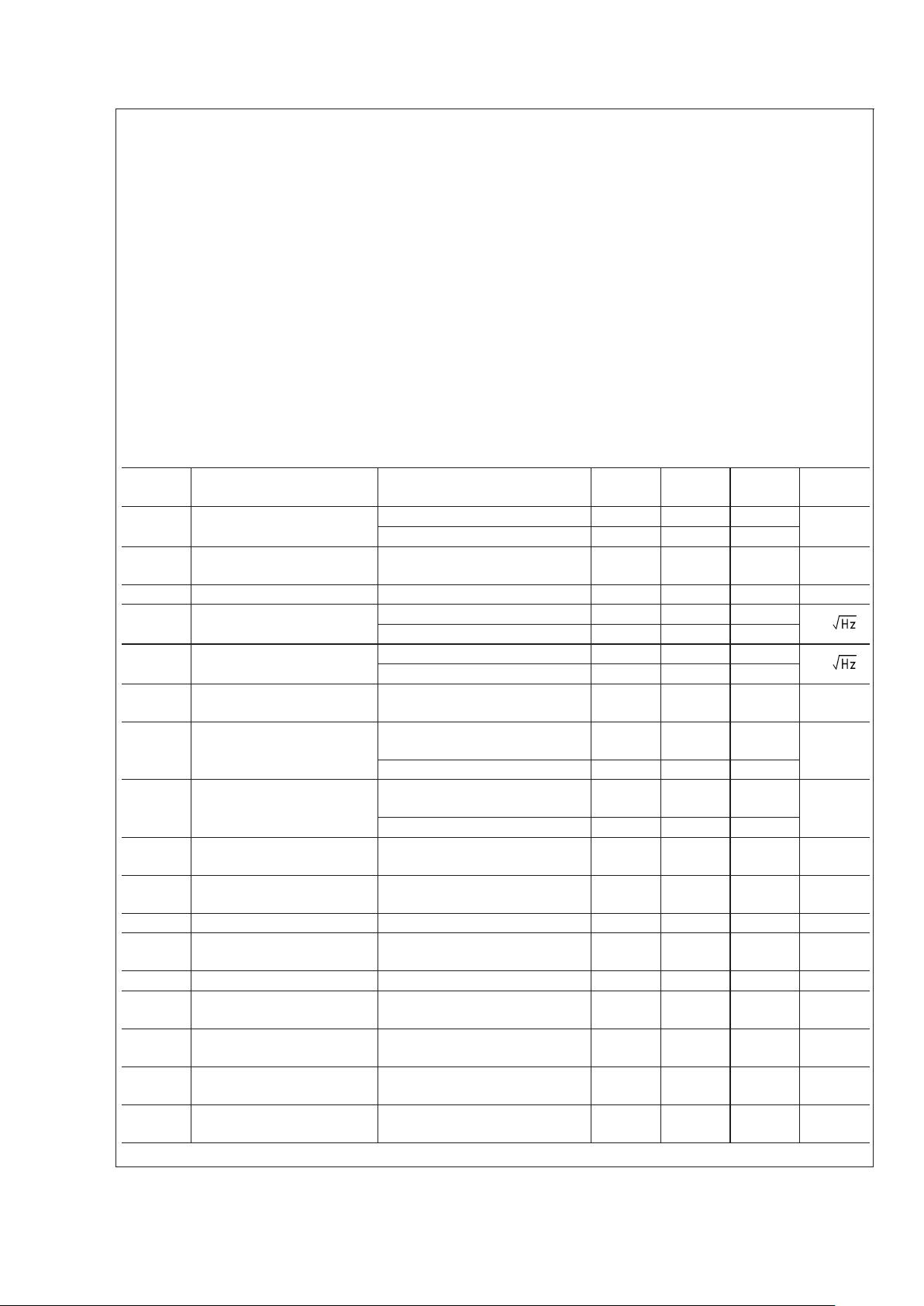
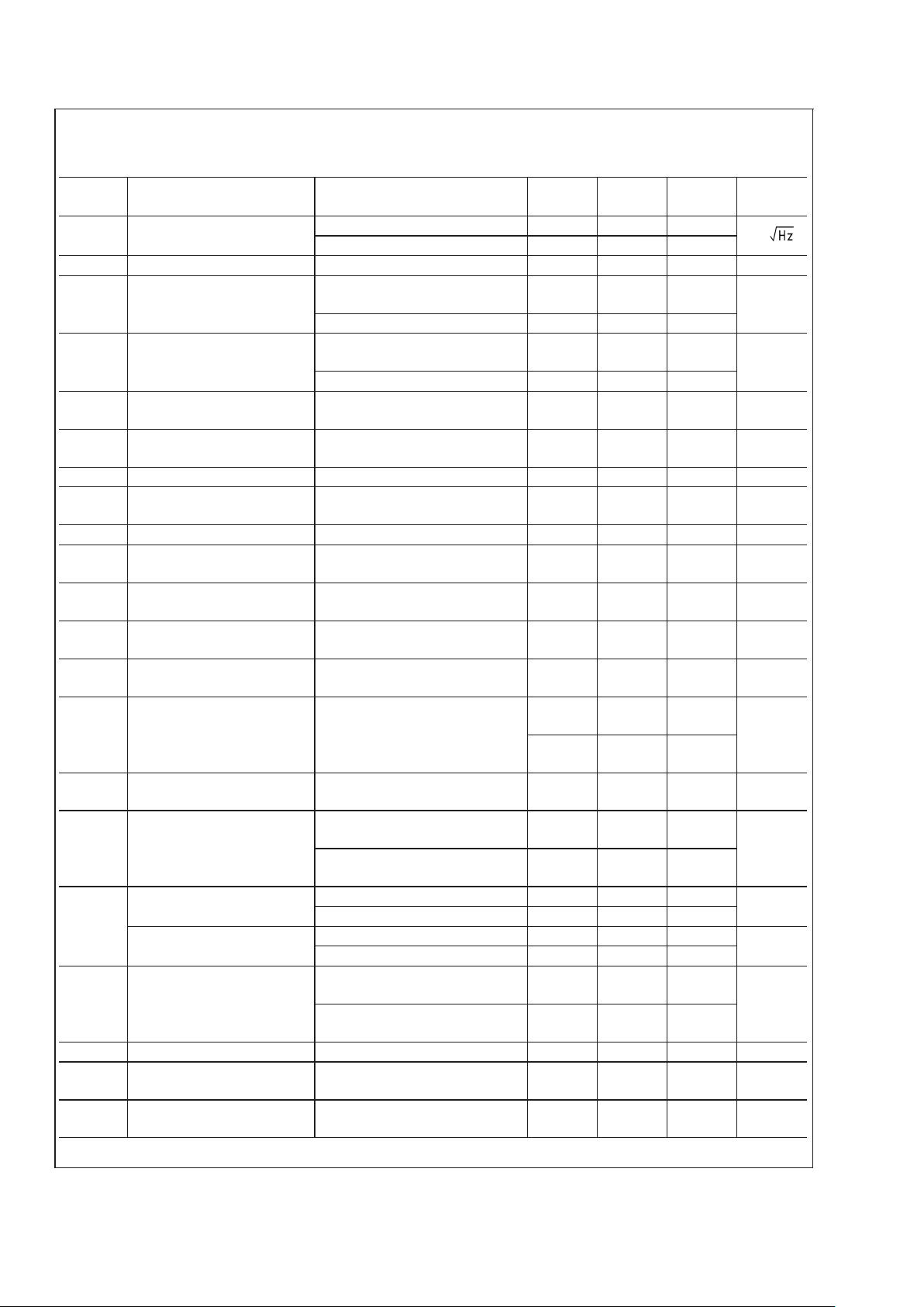
3V Electrical Characteristics
Unless otherwise specified, all limits guaranteed for at TJ= 25˚C, V+= 3V, V−= 0V, VCM=VO=V+/2, and RL=2kΩ to V+/2.
Boldface limits apply at the temperature extremes.
Symbol Parameter Conditions Min
(Note 6)
Typ
(Note 5)
Max
(Note 6)
Units
BW −3dB BW A
V
= +1, V
OUT
= 200mV
PP
80 115
MHz
A
V
= +2, −1, V
OUT
= 200mV
PP
46
BW
0.1dB
0.1dB Gain Flatness AV= +2, RL= 150Ω to V+/2,
R
L
= 402Ω,V
OUT
= 200mV
PP
19 MHz
PBW Full Power Bandwidth A
V
= +1, −1dB, V
OUT
=1V
PP
40 MHz
e
n
Input-Referred Voltage Noise f = 100kHz 17
nV/
f = 1kHz 48
i
n
Input-Referred Current Noise f = 100kHz 0.90
pA/
f = 1kHz 3.3
THD Total Harmonic Distortion f = 5MHz, V
O
=2VPP,AV= −1,
R
L
= 100Ω to V+/2
−48
dBc
DG Differential Gain V
CM
= 1V, NTSC, AV=+2
R
L
=150Ω to V+/2
0.17
%
R
L
=1kΩ to V+/2 0.03
DP Differential Phase V
CM
= 1V, NTSC, AV=+2
R
L
=150Ω to V+/2
0.05
deg
R
L
=1kΩ to V+/2 0.03
CT Rej. Cross-Talk Rejection f = 5MHz, Receiver:
R
f=Rg
= 510Ω,AV=+2
47 dB
T
S
Settling Time VO=2VPP,±0.1%, 8pF Load,
V
S
=5V
68 ns
SR Slew Rate (Note 8) A
V
= −1, VI=2V
PP
90 120 V/µs
V
OS
Input Offset Voltage
±
1
±
5
±
7
mV
TC V
OS
Input Offset Average Drift (Note 12)
±
5 µV/˚C
I
B
Input Bias Current (Note 7) −1.50 −2.60
−3.25
µA
I
OS
Input Offset Current 20 800
1000
nA
R
IN
Common Mode Input
Resistance
3MΩ
C
IN
Common Mode Input
Capacitance
2pF
LMH6642/6643/6644
www.national.com 2
3V Electrical Characteristics (Continued)
Unless otherwise specified, all limits guaranteed for at TJ= 25˚C, V+= 3V, V−= 0V, VCM=VO=V+/2, and RL=2kΩ to V+/2.
Boldface limits apply at the temperature extremes.
Symbol Parameter Conditions Min
(Note 6)
Typ
(Note 5)
Max
(Note 6)
Units
CMVR Input Common-Mode Voltage
Range
CMRR ≥ 50dB −0.5 −0.2
−0.1
V
1.8
1.6
2.0
CMRR Common Mode Rejection
Ratio
V
CM
Stepped from 0V to 1.5V 72 95 dB
A
VOL
Large Signal Voltage Gain VO= 0.5V to 2.5V
R
L
=2kΩ to V+/2
80
75
96
dB
V
O
= 0.5V to 2.5V
R
L
= 150Ω to V+/2
74
70
82
V
O
Output Swing
High
RL=2kΩ to V+/2, VID= 200mV 2.90 2.98
V
R
L
= 150Ω to V+/2, VID= 200mV 2.80 2.93
Output Swing
Low
R
L
=2kΩ to V+/2, VID= −200mV 25 75
mV
R
L
= 150Ω to V+/2, VID= −200mV 75 150
I
SC
Output Short Circuit Current Sourcing to V+/2
V
ID
= 200mV (Note 10)
50
35
95
mA
Sinking to V
+
/2
V
ID
= −200mV (Note 10)
55
40
110
I
OUT
Output Current V
OUT
= 0.5V from either supply
±
65 mA
+PSRR Positive Power Supply
Rejection Ratio
V
+
= 3.0V to 3.5V, VCM= 1.5V 75 85 dB
I
S
Supply Current (per channel) No Load 2.70 4.00
4.50
mA
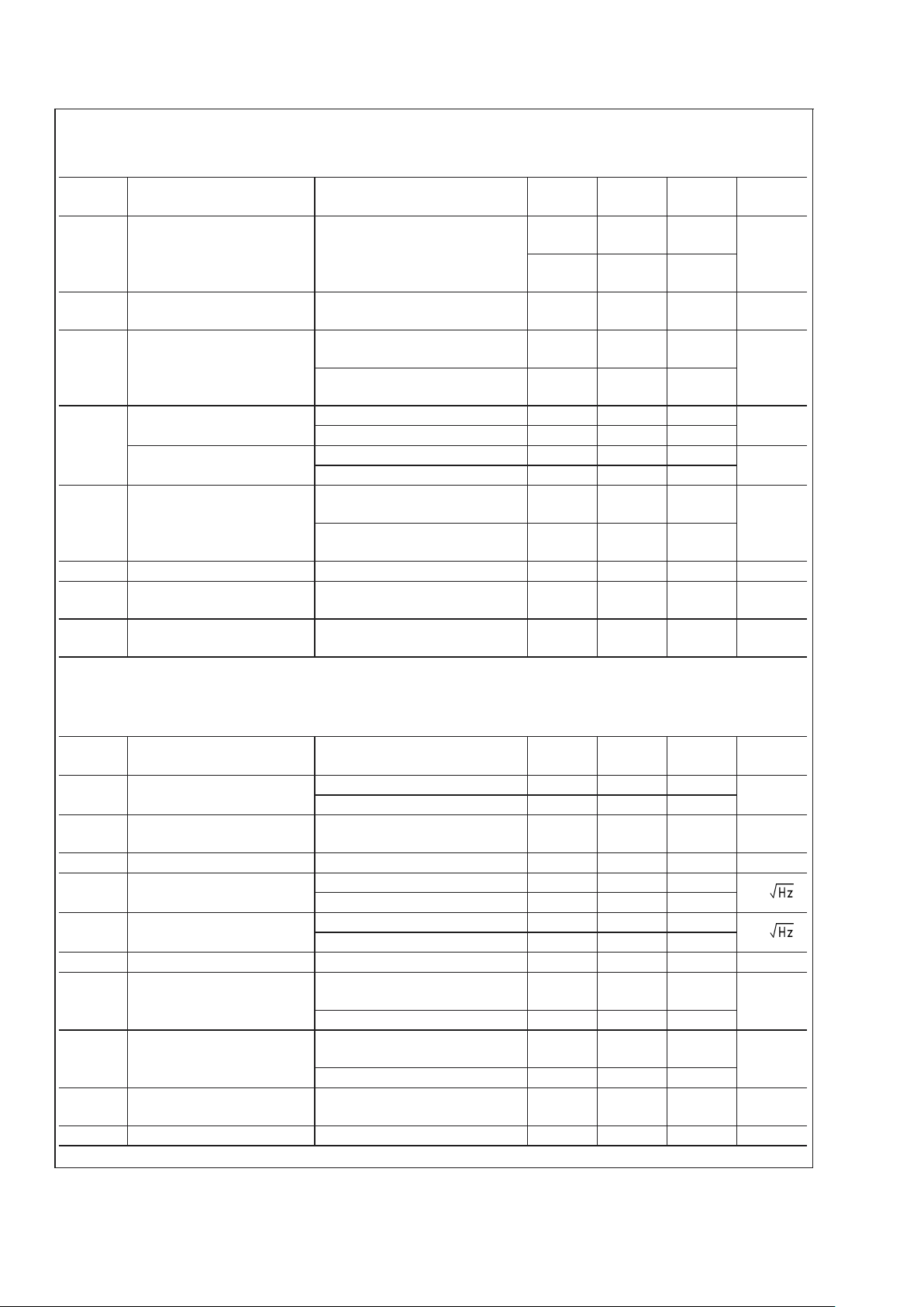
5V Electrical Characteristics
Unless otherwise specified, all limits guaranteed for at TJ= 25˚C, V+= 5V, V−= 0V, VCM=VO=V+/2, and RL=2kΩ to V+/2.
Boldface limits apply at the temperature extremes.
Symbol Parameter Conditions Min
(Note 6)
Typ
(Note 5)
Max
(Note 6)
Units
BW −3dB BW A
V
= +1, V
OUT
= 200mV
PP
90 120
MHz
A
V
= +2, −1, V
OUT
= 200mV
PP
46
BW
0.1dB
0.1dB Gain Flatness AV= +2, RL= 150Ω to V+/2,
R
f
= 402Ω,V
OUT
= 200mV
PP
15 MHz
PBW Full Power Bandwidth A
V
= +1, −1dB, V
OUT
=2V
PP
22 MHz
e
n
Input-Referred Voltage Noise f = 100kHz 17
nV/
f = 1kHz 48
i
n
Input-Referred Current Noise f = 100kHz 0.90
pA/
f = 1kHz 3.3
THD Total Harmonic Distortion f = 5MHz, V
O
=2VPP,AV= +2 −60 dBc
DG Differential Gain NTSC, A
V
=+2
R
L
=150Ω to V+/2
0.16
%
R
L
=1kΩ to V+/2 0.05
DP Differential Phase NTSC, A
V
=+2
R
L
=150Ω to V+/2
0.05
deg
R
L
=1kΩ to V+/2 0.01
CT Rej. Cross-Talk Rejection f = 5MHz, Receiver:
R
f=Rg
= 510Ω,AV=+2
47 dB
T
S
Settling Time VO=2VPP,±0.1%, 8pF Load 68 ns
LMH6642/6643/6644
www.national.com3
5V Electrical Characteristics (Continued)
Unless otherwise specified, all limits guaranteed for at TJ= 25˚C, V+= 5V, V−= 0V, VCM=VO=V+/2, and RL=2kΩ to V+/2.
Boldface limits apply at the temperature extremes.
Symbol Parameter Conditions Min
(Note 6)
Typ
(Note 5)
Max
(Note 6)
Units
SR Slew Rate (Note 8) A
V
= −1, VI=2V
PP
95 125 V/µs
V
OS
Input Offset Voltage
±
1
±
5
±
7
mV
TC V
OS
Input Offset Average Drift (Note 12)
±
5 µV/˚C
I
B
Input Bias Current (Note 7)
−1.70
−2.60
−3.25
µA
I
OS
Input Offset Current
20
800
1000
nA
R
IN
Common Mode Input
Resistance
3
MΩ
C
IN
Common Mode Input
Capacitance
2
pF
CMVR Input Common-Mode Voltage
Range
CMRR ≥ 50dB
−0.5
−0.2
−0.1
V
3.8
3.6
4.0
CMRR Common Mode Rejection
Ratio
V
CM
Stepped from 0V to 3.5V
72 95
dB
A
VOL
Large Signal Voltage Gain VO= 0.5V to 4.50V
R
L
=2kΩ to V+/2
86
82
98
dB
V
O
= 0.5V to 4.25V
R
L
= 150Ω to V+/2
76
72
82
V
O
Output Swing
High
RL=2kΩ to V+/2, VID= 200mV 4.90 4.98
V
R
L
= 150Ω to V+/2, VID= 200mV 4.65 4.90
Output Swing
Low
R
L
=2kΩ to V+/2, VID= −200mV 25 100
mV
R
L
= 150Ω to V+/2, VID= −200mV 100 150
I
SC
Output Short Circuit Current Sourcing to V+/2
V
ID
= 200mV (Note 10)
55
40
115
mA
Sinking to V
+
/2
V
ID
= −200mV (Note 10)
70
55
140
I
OUT
Output Current VO= 0.5V from either supply
±
70 mA
+PSRR Positive Power Supply
Rejection Ratio
V
+
= 4.0V to 6V
79 90
dB
I
S
Supply Current (per channel) No Load
2.70
4.25
5.00
mA
±
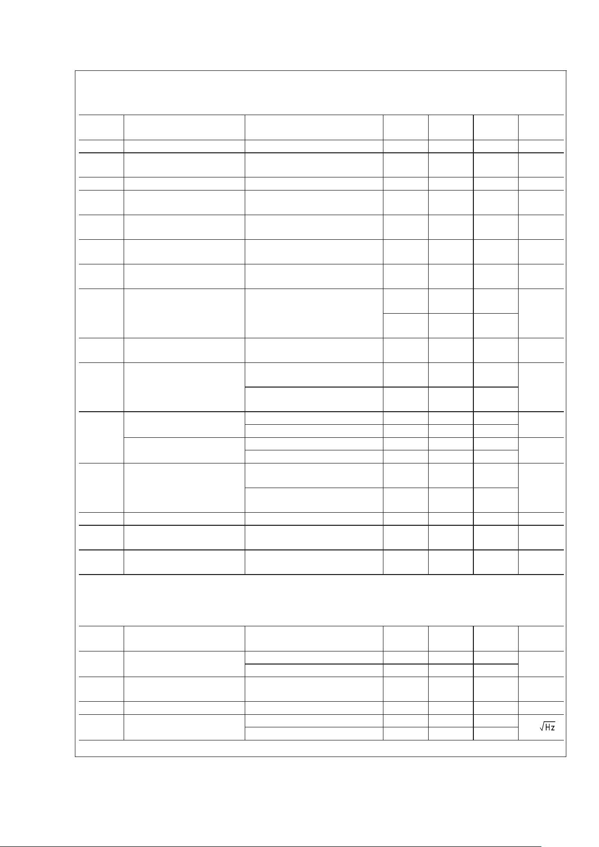
5V Electrical Characteristics
Unless otherwise specified, all limits guaranteed for at TJ= 25˚C, V+= 5V, V−= −5V, VCM=VO= 0V and RL=2kΩ to ground.
Boldface limits apply at the temperature extremes.
Symbol Parameter Conditions Min
(Note 6)
Typ
(Note 5)
Max
(Note 6)
Units
BW −3dB BW A
V
= +1, V
OUT
= 200mV
PP
95 130
MHz
A
V
= +2, −1, V
OUT
= 200mV
PP
46
BW
0.1dB
0.1dB Gain Flatness AV= +2, RL= 150Ω to V+/2,
R
f
= 806Ω,V
OUT
= 200mV
PP
12 MHz
PBW Full Power Bandwidth A
V
= +1, −1dB, V
OUT
=2V
PP
24 MHz
e
n
Input-Referred Voltage Noise f = 100kHz 17
nV/
f = 1kHz 48
LMH6642/6643/6644
www.national.com 4
±
5V Electrical Characteristics (Continued)
Unless otherwise specified, all limits guaranteed for at TJ= 25˚C, V+= 5V, V−= −5V, VCM=VO= 0V and RL=2kΩ to ground.
Boldface limits apply at the temperature extremes.
Symbol Parameter Conditions Min
(Note 6)
Typ
(Note 5)
Max
(Note 6)
Units
i
n
Input-Referred Current Noise f = 100kHz 0.90
pA/
f = 1kHz 3.3
THD Total Harmonic Distortion f = 5MHz, V
O
=2VPP,AV= +2 −62 dBc
DG Differential Gain NTSC, A
V
=+2
R
L
=150Ω to V+/2
0.15
%
R
L
=1kΩ to V+/2 0.01
DP Differential Phase NTSC, A
V
=+2
R
L
=150Ω to V+/2
0.04
deg
R
L
=1kΩ to V+/2 0.01
CT Rej. Cross-Talk Rejection f = 5MHz, Receiver:
Rf=Rg= 510Ω,AV=+2
47 dB
T
S
Settling Time VO=2VPP,±0.1%, 8pF Load,
V
S
=5V
68
ns
SR Slew Rate (Note 8) A
V
= −1, VI=2V
PP
100 135 V/µs
V
OS
Input Offset Voltage
±
1
±
5
±
7
mV
TC V
OS
Input Offset Average Drift (Note 12)
±
5 µV/˚C
I
B
Input Bias Current (Note 7)
−1.60
−2.60
−3.25
µA
I
OS
Input Offset Current
20
800
1000
nA
R
IN
Common Mode Input
Resistance
3
MΩ
C
IN
Common Mode Input
Capacitance
2
pF
CMVR Input Common-Mode Voltage
Range
CMRR ≥ 50dB
−5.5
−5.2
−5.1
V
3.8
3.6
4.0
CMRR Common Mode Rejection
Ratio
V
CM
Stepped from −5V to 3.5V
74 95
dB
A
VOL
Large Signal Voltage Gain VO= −4.5V to 4.5V,
R
L
=2kΩ
88
84
96
dB
V
O
= −4.0V to 4.0V,
R
L
= 150Ω
78
74
82
V
O
Output Swing
High
RL=2kΩ,VID= 200mV 4.90 4.96
V
R
L
= 150Ω,VID= 200mV 4.65 4.80
Output Swing
Low
R
L
=2kΩ,VID= −200mV −4.96 −4.90
V
R
L
= 150Ω,VID= −200mV −4.80 −4.65
I
SC
Output Short Circuit Current Sourcing to Ground
V
ID
= 200mV (Note 10)
60
35
115
mA
Sinking to Ground
V
ID
= −200mV (Note 10)
85
65
145
I
OUT
Output Current VO= 0.5V from either supply
±
75 mA
PSRR Power Supply Rejection Ratio (V
+,V−
) = (4.5V, −4.5V) to (5.5V,
−5.5V)
78 90
dB
I
S
Supply Current (per channel) No Load
2.70
4.50
5.50
mA
LMH6642/6643/6644
www.national.com5
±
5V Electrical Characteristics (Continued)
Note 1: Absolute Maximum Ratings indicate limits beyond which damage to the device may occur. Operating Ratings indicate conditions for which the device is
intended to be functional, but specific performance is not guaranteed. For guaranteed specifications and the test conditions, see the Electrical Characteristics.
Note 2: Human body model, 1.5kΩ in series with 100pF.
Note 3: Applies to both single-supply and split-supply operation. Continuous short circuit operation at elevated ambient temperature can result in exceeding the
maximum allowed junction temperature of 150˚C.
Note 4: The maximum power dissipation is a function of T
J(MAX)
, θJA, and TA. The maximum allowable power dissipation at any ambient temperature is
P
D
=(T
J(MAX)-TA
)/ θJA. All numbers apply for packages soldered directly onto a PC board.
Note 5: Typical values represent the most likely parametric norm.
Note 6: All limits are guaranteed by testing or statistical analysis.
Note 7: Positive current corresponds to current flowing into the device.
Note 8: Slew rate is the average of the rising and falling slew rates.
Note 9: Machine Model, 0Ω in series with 200pF.
Note 10: Short circuit test is a momentary test. See Note 11.
Note 11: Output short circuit duration is infinite for V
S
<
6V at room temperature and below. For V
S
>
6V, allowable short circuit duration is 1.5ms.
Note 12: Offset voltage average drift determined by dividing the change in V
OS
at temperature extremes by the total temperature change.
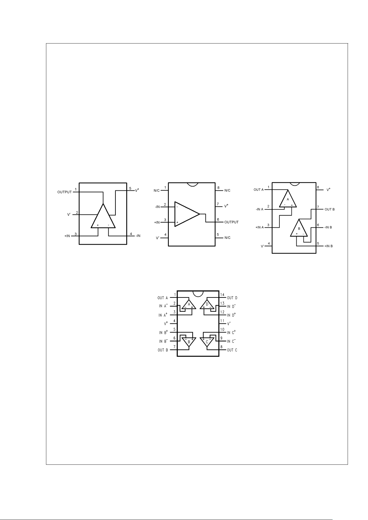
Connection Diagrams
SOT23-5 (LMH6642) SOIC-8 (LMH6642)
SOIC-8 and MSOP-8
(LMH6643)
20018561
Top View
20018562
Top View
20018563
Top View
SOIC-14 and TSSOP-14
(LMH6644)
20018568
Top View
LMH6642/6643/6644
www.national.com 6
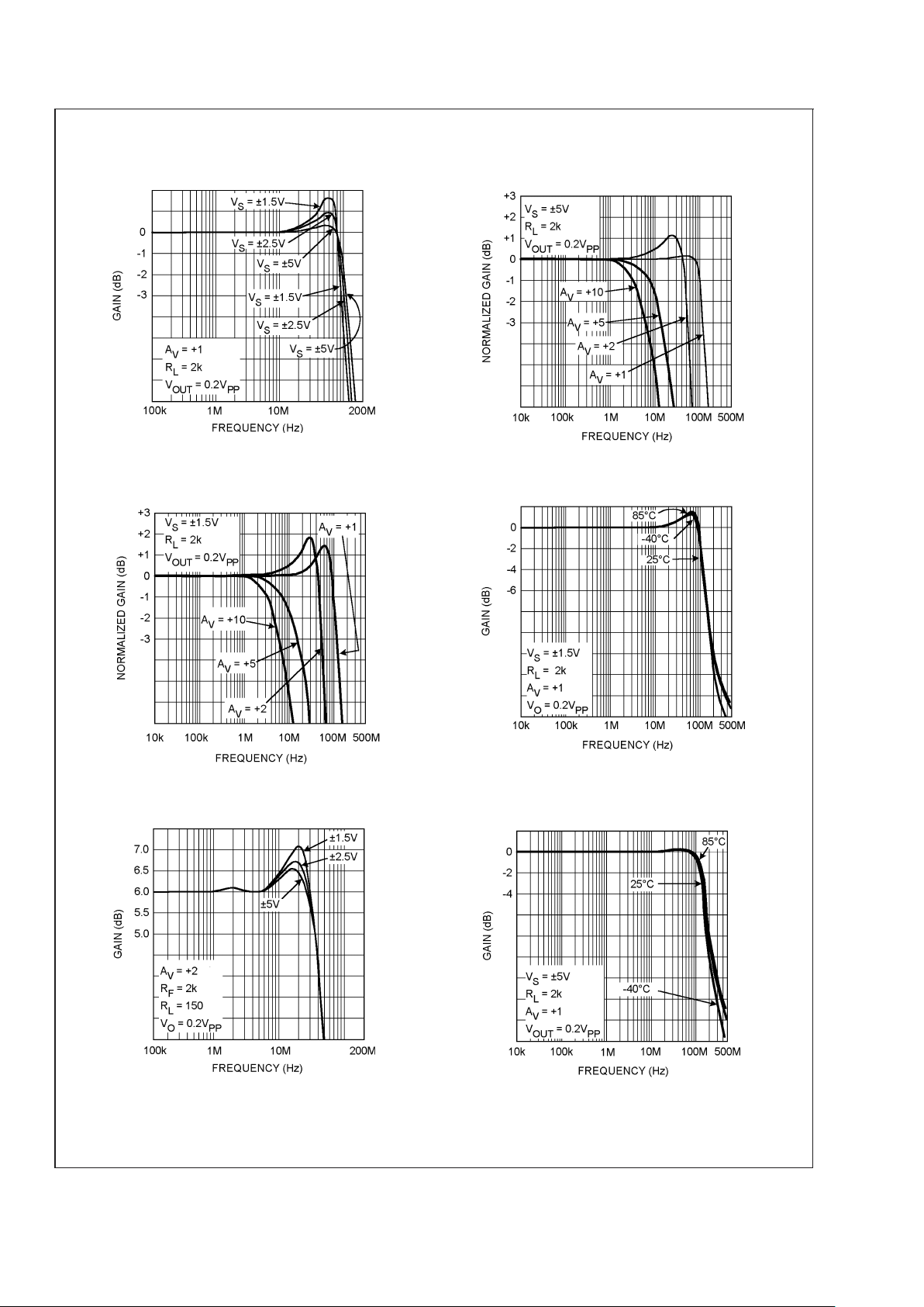
Typical Performance Characteristics At T
J
= 25˚C, V+= +5, V−= −5V, RF=RL=2kΩ. Unless
otherwise specified.
Closed Loop Frequency Response for Various Supplies Closed Loop Gain vs. Frequency for Various Gain
20018557
20018551
Closed Loop Gain vs. Frequency for Various Gain
Closed Loop Frequency Response for Various
Temperature
20018535
20018550
Closed Loop Gain vs. Frequency for Various Supplies
Closed Loop Frequency Response for Various
Temperature
20018548
20018534
LMH6642/6643/6644
www.national.com7
 Loading...