

NSC LMH6628MDC, LMH6628MAX, LMH6628MA Datasheet
LMH6628
Dual Wideband, Low Noise, Voltage Feedback Op Amp
General Description
The National LMH6628 is a high speed dual op amp that
offers a traditional voltage feedback topology featuring unity
gain stability and slew enhanced circuitry. The LMH6628’s
low noise and very low harmonic distortion combine to form
a wide dynamic range op amp that operates from a single
(5V to 12V) or dual (
±
5V) power supply.
Each of the LMH6628’s closely matched channels provides
a 300MHz unity gain bandwidth and low input voltage noise
density (2nV/
). Low 2nd/3rd harmonic distortion (−65/
−74dBc at 10MHz) make the LMH6628 a perfect wide dynamic range amplifier for matched I/Q channels.
With its fast and accurate settling (12ns to 0.1%), the
LMH6628 is also an excellent choice for wide dynamic
range, anti-aliasing filters to buffer the inputs of hi resolution
analog-to-digital converters. Combining the LMH6628’s two
tightly matched amplifiers in a single 8-pin SOIC package
reduces cost and board space for many composite amplifier
applications such as active filters, differential line drivers/
receivers, fast peak detectors and instrumentation amplifiers.
The LMH6628 is fabricated using National’s VIP10
™
com-
plimentary bipolar process.
To reduce design times and assist in board layout, the
LMH6628 is supported by an evaluation board
(CLC730036).
Features
n Wide unity gain bandwidth: 300MHz
n Low noise: 2nV/
n Low Distortion: −65/−74dBc (10MHz)
n Settling time: 12ns to 0.1%
n Wide supply voltage range:
±
2.5V to±6V
n High output current:
±
85mA
n Improved replacement for CLC428
Applications
n High speed dual op amp
n Low noise integrators
n Low noise active filters
n Driver/receiver for transmission systems
n High speed detectors
n I/Q channel amplifiers
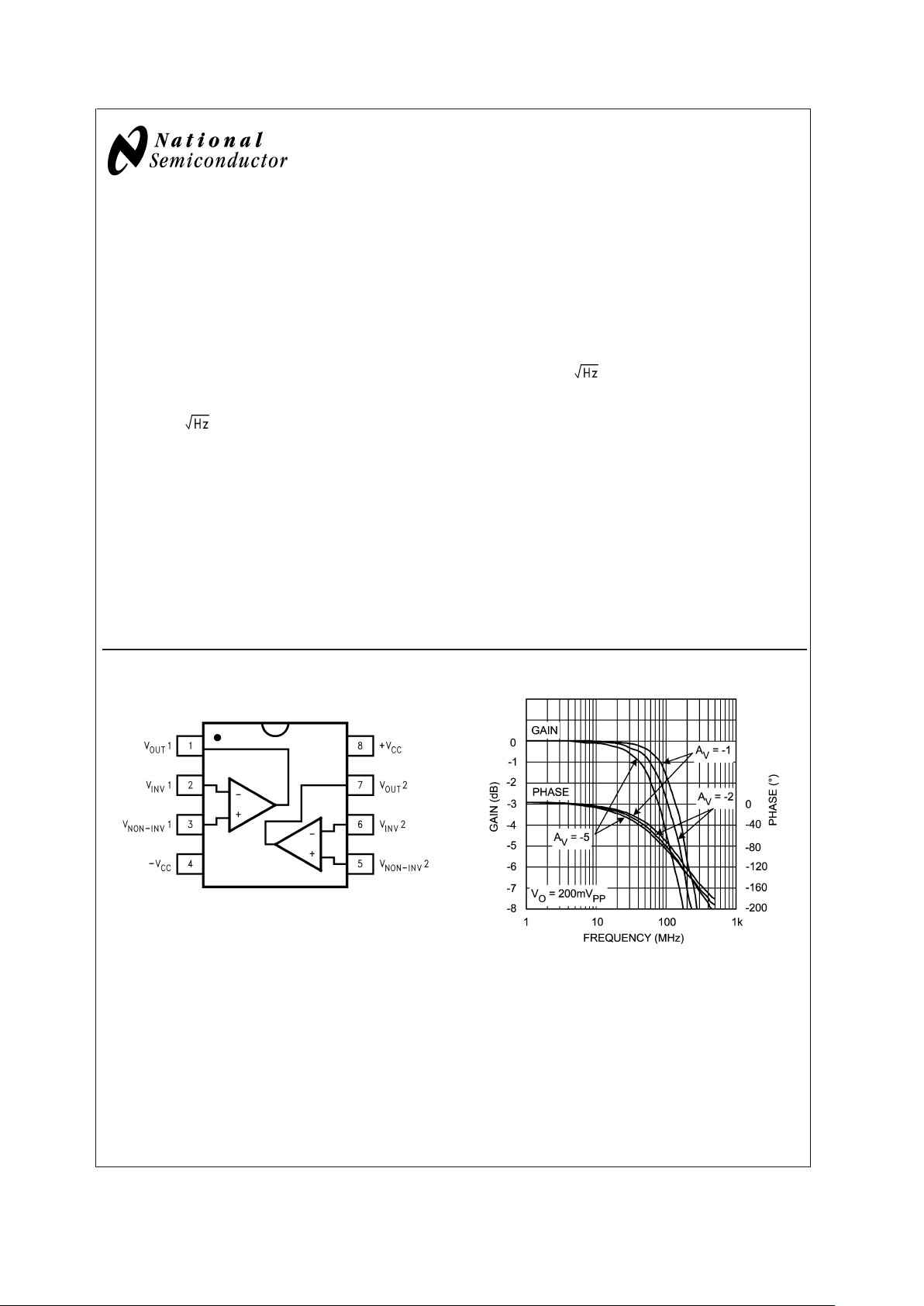
Connection Diagram
8-Pin SOIC
20038535
Top View
Inverting Frequency Response
20038515
January 2003
LMH6628 Dual Wideband, Low Noise, Voltage Feedback Op Amp
© 2003 National Semiconductor Corporation DS200385 www.national.com
Absolute Maximum Ratings (Note 1)
If Military/Aerospace specified devices are required,
please contact the National Semiconductor Sales Office/
Distributors for availability and specifications.
ESD Tolerance (Note 4)
Human Body Model 2kV
Machine Model 200V
Supply Voltage 13.5
Short Circuit Current (Note 3)
Common-Mode Input Voltage V
+-V−
Differential Input Voltage V+-V
−
Maximum Junction Temperature +150˚C
Storage Temperature Range −65˚C to +150˚C
Lead Temperature (soldering 10 sec) +300˚C
Operating Ratings (Note 1)
Thermal Resistance (Note 5)
Package (θ
JC
)(θJA)
SOIC 65˚C/W 145˚C/W
Temperature Range −40˚C to +85˚C
Nominal Supply Voltage
±
2.5V to±6V
Electrical Characteristics (Note 2)
VCC=±5V, AV= +2V/V, RF= 100Ω,RG= 100Ω,RL= 100Ω; unless otherwise specified. Boldface limits apply at the
temperature extremes.
Symbol Parameter Conditions Min Typ Max Units
Frequency Domain Response
GB Gain Bandwidth Product V
O
<
0.5V
PP
200 MHz
SSBW -3dB Bandwidth, A
V
=+1 V
O
<
0.5V
PP
180 300 MHz
SSBW -3dB Bandwidth, A
V
=+2 V
O
<
0.5V
PP
100 MHz
GFL Gain Flatness V
O
<
0.5V
PP
GFP Peaking DC to 200MHz 0.0 dB
GFR Rolloff DC to 20MHz .1 dB
LPD Linear Phase Deviation DC to 20MHz .1 deg
Time Domain Response
TR Rise and Fall Time 1V Step 4 ns
TS Settling Time 2V Step to 0.1% 12 ns
OS Overshoot 1V Step 1 %
SR Slew Rate 4V Step 300 550 V/µs
Distortion And Noise Response
HD2 2nd Harmonic Distortion 1V
PP
, 10MHz −65 dBc
HD3 3rd Harmonic Distortion 1V
PP
, 10MHz −74 dBc
Equivalent Input Noise
V
N
Voltage 1MHz to 100MHz 2 nV/
I
N
Current 1MHz to 100MHz 2 pA/
XTLKA Crosstalk Input Referred, 10MHz −62 dB
Static, DC Performance
G
OL
Open-Loop Gain 56
53
63 dB
V
IO
Input Offset Voltage
±
.5
±
2
±
2.6
mV
DV
IO
Average Drift 5 µV/˚C
I
BN
Input Bias Current
±
.7
±
20
±
30
µA
DI
BN
Average Drift 150 nA/˚C
I
OS
Input Offset Current 0.3
±
6µA
I
OSD
Average Drift 5 nA/˚C
PSRR Power Supply Rejection Ratio 60
46
70 dB
CMRR Common-Mode Rejection Ratio 57
54
62 dB
I
CC
Supply Current Per Channel, RL=
∞
7.5
7.0
912
12.5
mA
LMH6628
www.national.com 2
Electrical Characteristics (Note 2) (Continued)
VCC=±5V, AV= +2V/V, RF= 100Ω,RG= 100Ω,RL= 100Ω; unless otherwise specified. Boldface limits apply at the
temperature extremes.
Symbol Parameter Conditions Min Typ Max Units
Miscellaneous Performance
R
IN
Input Resistance Common-Mode 500 kΩ
Differential-Mode 200 kΩ
C
IN
Input Capacitance Common-Mode 1.5 pF
Differential-Mode 1.5 pF
R
OUT
Output Resistance Closed-Loop .1 Ω
V
O
Output Voltage Range RL=
∞
±
3.8 V
V
OL
RL= 100Ω
±
3.2
±
3.1
±
3.5 V
CMIR Input Voltage Range Common- Mode
±
3.7 V
I
O
Output Current
±
50
±
85 mA
Note 1: Absolute Maximum Ratings indicate limits beyond which damage to the device may occur. Operating Ratings indicate conditions for which the device is
intended to be functional, but specific performance is not guaranteed. For guaranteed specifications, see the Electrical Characteristics tables.
Note 2: Electrical Table values apply only for factory testing conditions at the temperature indicated. Factory testing conditions result in very limited self-heating of
the device such that T
J=TA
. No guarantee of parametric performance is indicated in the electrical tables under conditions of internal self heating where T
J
>
TA.
See Note 6 for information on temperature de-rating of this device." Min/Max ratings are based on product characterization and simulation. Individual parameters
are tested as noted.
Note 3: Output is short circuit protected to ground, however maximum reliability is obtained if output current does not exceed 160mA.
Note 4: Human body model, 1.5kΩ in series with 100pF. Machine model, 0Ω In series with 200pF.
Note 5: The maximum power dissipation is a function of T
J(MAX)
, θJAand TA. The maximum allowable power dissipation at any ambient temperature is
P
D
=(T
J(MAX)-TA
)/ θJA. All numbers apply for packages soldered directly onto a PC board.
Ordering Information
Package Part Number Package Marking Transport Media NSC Drawing
8-pin SOIC LMH6628MA LMH6628MA Rails M08A
LMH6628MAX 2.5k Units Tape and Reel
LMH6628
www.national.com3
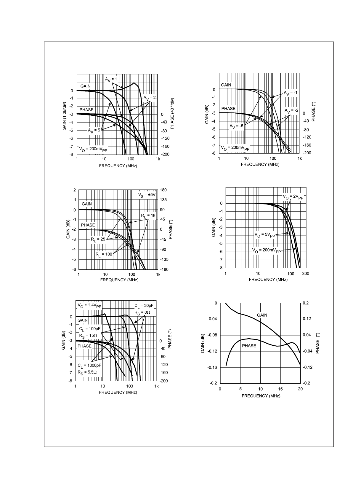
Typical Performance Characteristics (T
A
= +25˚, AV= +2, VCC=±5V, Rf=100Ω,RL= 100Ω, un-
less specified)
Non-Inverting Frequency Response Inverting Frequency Response
20038513
20038515
Frequency Response vs. Load Resistance Frequency Response vs. Output Amplitude
20038525
20038510
Frequency Response vs. Capacitive Load Gain Flatness & Linear Phase
20038516
20038524
LMH6628
www.national.com 4
 Loading...