

NSC LMH6622MMX, LMH6622MM, LMH6622MAX, LMH6622MA, LMH6622MWC Datasheet
LMH6622
Dual Wideband, Low Noise, 160MHz, Operational
Amplifiers
General Description
The LMH6622 is a dual high speed voltage feedback operational amplifier specifically optimized for lownoise.A voltage
noise specification of 1.6nV/
, a current noise specifi-
cation 1.5pA/
, abandwidth of 160MHz,and a harmonic
distortion specificationthat exceeds 90dBc combineto make
the LMH6622 an ideal choice for the receive channel amplifier in ADSL, VDSL, or other xDSL designs. The LMH6622
operates from
±
2.5V to±6V in dual supply mode and from
+5V to +12V in single supply configuration. The LMH6622 is
stable for A
V
≥ 2orAV≤−1. The fabrication of the LMH6622
on National Semiconductor’s advanced VIP10 process enables excellent (160MHz) bandwidth at a current consumption of only 4.3mA/amplifier. Packages for this dual amplifier
are the 8-lead SOIC and the 8-lead MSOP.
Features
VS=±6V, TA= 25˚C, Typical values unless specified
n Bandwidth (A
V
= +2) 160MHz
n Supply Voltage Range
±
2.5V to±6V +5V to +12
n Slew rate 85V/µs
n Supply current 4.3mA/amp
n Input common mode voltage −4.75V to +5.7V
n Output Voltage Swing (R
L
= 100Ω)
±
4.6V
n Input voltage noise 1.6nV/
n Input current noise 1.5pA/
n Linear output current 90mA
n Excellent harmonic distortion 90dBc
Applications
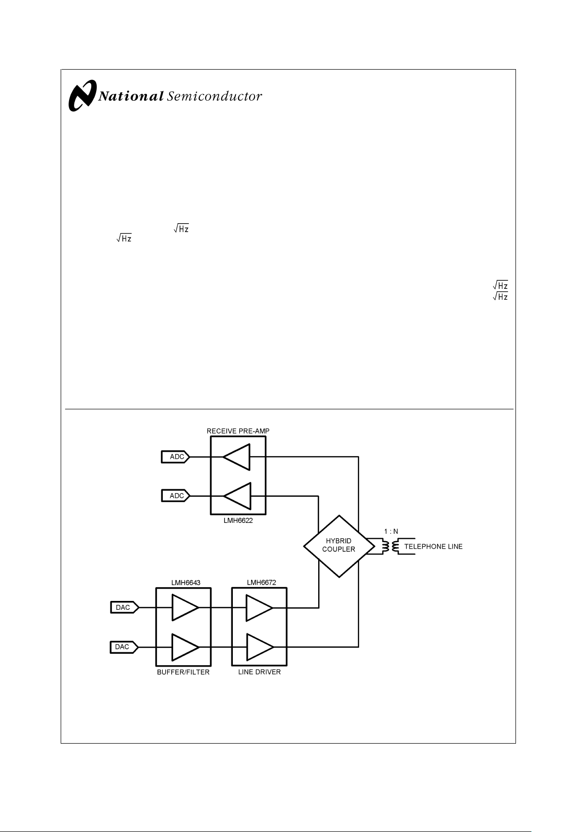
n xDSL receiver
n Low noise instrumentation front end
n Ultrasound preamp
n Active filters
n Cellphone basestation
20029226
xDSL Analog Front End
February 2002
LMH6622 Dual Wideband, Low Noise, 160MHz, Operational Amplifiers
© 2002 National Semiconductor Corporation DS200292 www.national.com
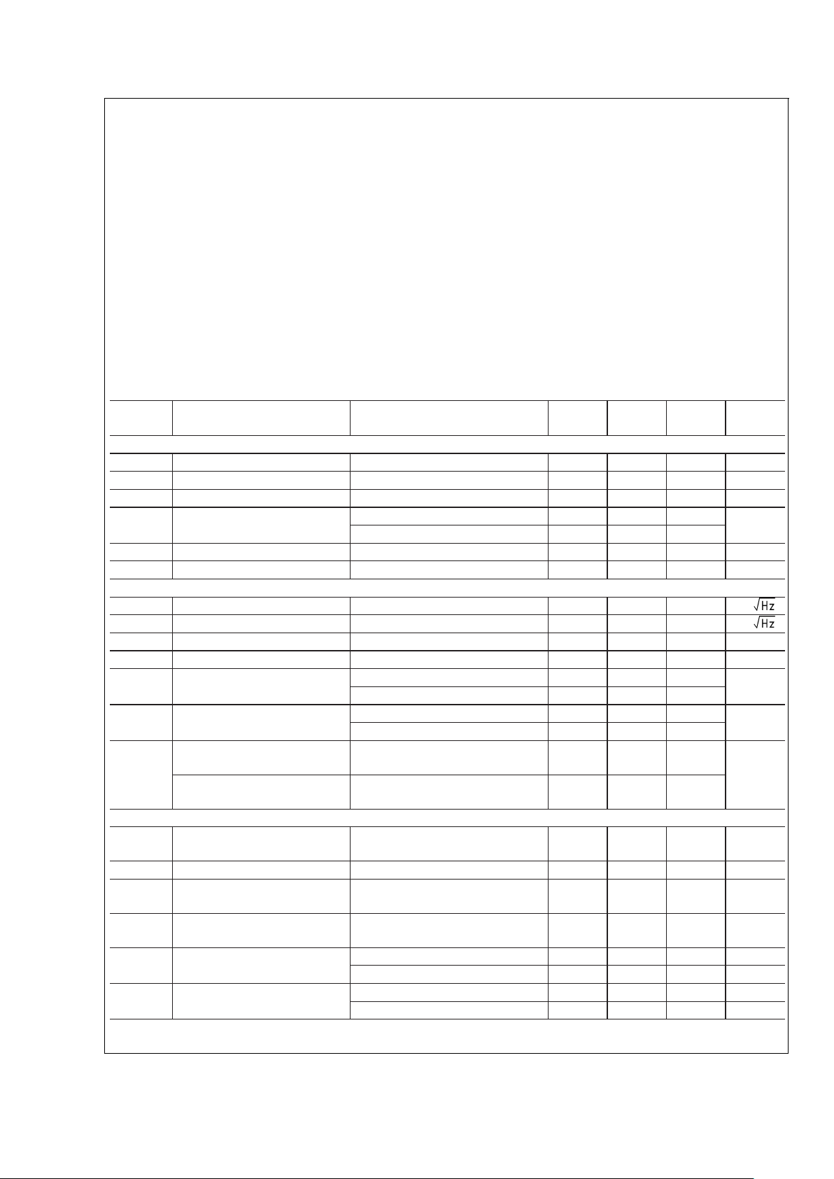
Absolute Maximum Ratings (Note 1)
If Military/Aerospace specified devices are required,
please contact the National Semiconductor Sales Office/
Distributors for availability and specifications.
ESD Tolerance
Human Body Model 2kV (Note 2)
Machine Model 200V (Note 2)
V
IN
Differential
±
1.2V
Supply Voltage (V
+–V−
) 13.2V
Voltage at Input Pins V
+
+0.5V, V−−0.5V
Soldering Information
Infrared or Convection (20 sec) 235˚C
Wave Soldering (10 sec) 260˚C
Storage Temperature Range −65˚C to +150˚C
Junction Temperature (Note 4) +150˚C
Operating Ratings (Note 1)
Supply Voltage (V
+–V−
)
±
2.25V to±6V
Junction Temperature Range
(Note 3), (Note 4)
−40˚C to +85˚C
Package Thermal Resistance (Note 4) (θ
JA
)
8-pin SOIC 166˚C/W
8-pin MSOP 211˚C/W
±
6V Electrical Characteristics
Unless otherwise specified, TJ= 25˚C, V+= 6V, V−= −6V, VCM= 0V, AV= +2, RF= 500Ω,RL= 100Ω. Boldface limits apply
at the temperature extremes.
Symbol Parameter Conditions Min
(Note 6)
Typ
(Note 5)
Max
(Note 6)
Units
Dynamic Performance
f
CL
−3dB BW VO= 200mV
PP
160 MHz
BW
0.1dB
0.1dB Gain Flatness VO= 200mV
PP
30 MHz
SR Slew Rate (Note 8) V
O
=2V
PP
85 V/µs
TS Settling Time V
O
=2VPPto±0.1% 40
ns
V
O
=2VPPto±1.0% 35
Tr Rise Time V
O
= 0.2V Step, 10% to 90% 2.3 ns
Tf Fall Time V
O
= 0.2V Step, 10% to 90% 2.3 ns
Distortion and Noise Response
e
n
Input Referred Voltage Noise f = 100kHz 1.6 nV/
i
n
Input Referred Current Noise f = 100kHz 1.5 pA/
DG Differential Gain RL= 150Ω,RF= 470Ω, NTSC 0.03 %
DP Differential Phase R
L
= 150Ω,RF= 470Ω, NTSC 0.03 deg
HD2 2
nd
Harmonic Distortion fc= 1MHz, VO=2VPP,RL= 100Ω −90
dBc
f
c
= 1MHz, VO=2VPP,RL= 500Ω −100
HD3 3
rd
Harmonic Distortion fc= 1MHz, VO=2VPP,RL= 100Ω −94
dBc
f
c
= 1MHz, VO=2VPP,RL= 500Ω −100
MTPR Upstream V
O
= 0.6 V
RMS
, 26kHz to 132kHz
(see test circuit 5)
−78
dBc
Downstream V
O
= 0.6 V
RMS
, 144kHz to 1.1MHz
(see test circuit 5)
−70
Input Characteristics
V
OS
Input Offset Voltage VCM= 0V −1.2
−2
+0.2 +1.2
+2
mV
TC V
OS
Input Offset Average Drift VCM= 0V (Note 7) −2.5 µV/˚C
I
OS
Input Offset Current VCM=0V −1
−1.5
−0.04 1
1.5
µA
I
B
Input Bias Current VCM= 0V 4.7 10
15
µA
R
IN
Input Resistance Common Mode 17 MΩ
Differential Mode 12 kΩ
C
IN
Input Capacitance Common Mode 0.9 pF
Differential Mode 1.0 pF
LMH6622
www.national.com 2
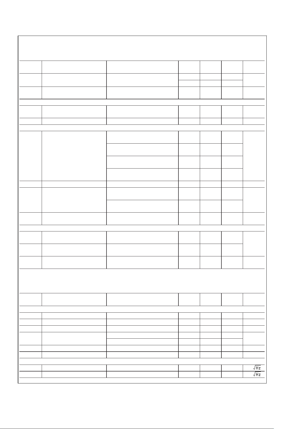
±
6V Electrical Characteristics (Continued)
Unless otherwise specified, TJ= 25˚C, V+= 6V, V−= −6V, VCM= 0V, AV= +2, RF= 500Ω,RL= 100Ω. Boldface limits apply
at the temperature extremes.
Symbol Parameter Conditions Min
(Note 6)
Typ
(Note 5)
Max
(Note 6)
Units
CMVR Input Common Mode Voltage
Range
CMRR ≥ 60dB −4.75 −4.5
V
5.5 +5.7
CMRR Common-Mode Rejection Ratio Input Referred,
V
CM
= −4.2 to +5.2V
80
75
100 dB
Transfer Characteristics
A
VOL
Large Signal Voltage Gain VO=4V
PP
74
70
83 dB
X
t
Crosstalk f = 1MHz −75 dB
Output Characteristics
V
O
Output Swing No Load, Positive Swing 4.8
4.6
5.2
V
No Load, Negative Swing −5.0 −4.6
−4.4
R
L
= 100Ω, Positive Swing 4.0
3.8
4.6
R
L
= 100Ω, Negative Swing −4.6 −4
−3.8
R
O
Output Impedance f = 1MHz 0.08 Ω
I
SC
Output Short Circuit Current Sourcing to Ground
∆V
IN
= 200mV (Note 3), (Note 9)
100 135
mA
Sinking to Ground
∆V
IN
= −200mV (Note 3), (Note 9)
100 130
I
OUT
Output Current Sourcing, VO= +4.3V
Sinking, V
O
= −4.3V
90 mA
Power Supply
+PSRR Positive Power Supply
Rejection Ratio
Input Referred,
V
S
= +5V to +6V
80
74
95
dB
−PSRR Negative Power Supply
Rejection Ratio
Input Referred,
V
S
= −5V to −6V
75
69
90
I
S
Supply Current (per amplifier) No Load 4.3 6
6.5
mA
±
2.5V Electrical Characteristics
Unless otherwise specified, all limits guaranteed for TJ= 25˚C, V+= 2.5V, V−= −2.5V, VCM= 0V, AV= +2, RF= 500Ω,
R
L
= 100Ω. Boldface limits apply at the temperature extremes.
Symbol Parameter Conditions Min
(Note 6)
Typ
(Note 5)
Max
(Note 6)
Units
Dynamic Performance
f
CL
−3dB BW VO= 200mV
PP
150 MHz
BW
0.1dB
0.1dB Gain Flatness VO= 200mV
PP
20 MHz
SR Slew Rate (Note 8) V
O
=2V
PP
80 V/µs
T
S
Settling Time VO=2VPPto±0.1% 45
ns
V
O
=2VPPto±1.0% 40
T
r
Rise Time VO= 0.2V Step, 10% to 90% 2.5 ns
T
f
Fall Time VO= 0.2V Step, 10% to 90% 2.5 ns
Distortion and Noise Response
e
n
Input Referred Voltage Noise f = 100kHz 1.7 nV/
i
n
Input Referred Current Noise f = 100kHz 1.5 pA/
LMH6622
www.national.com3
±
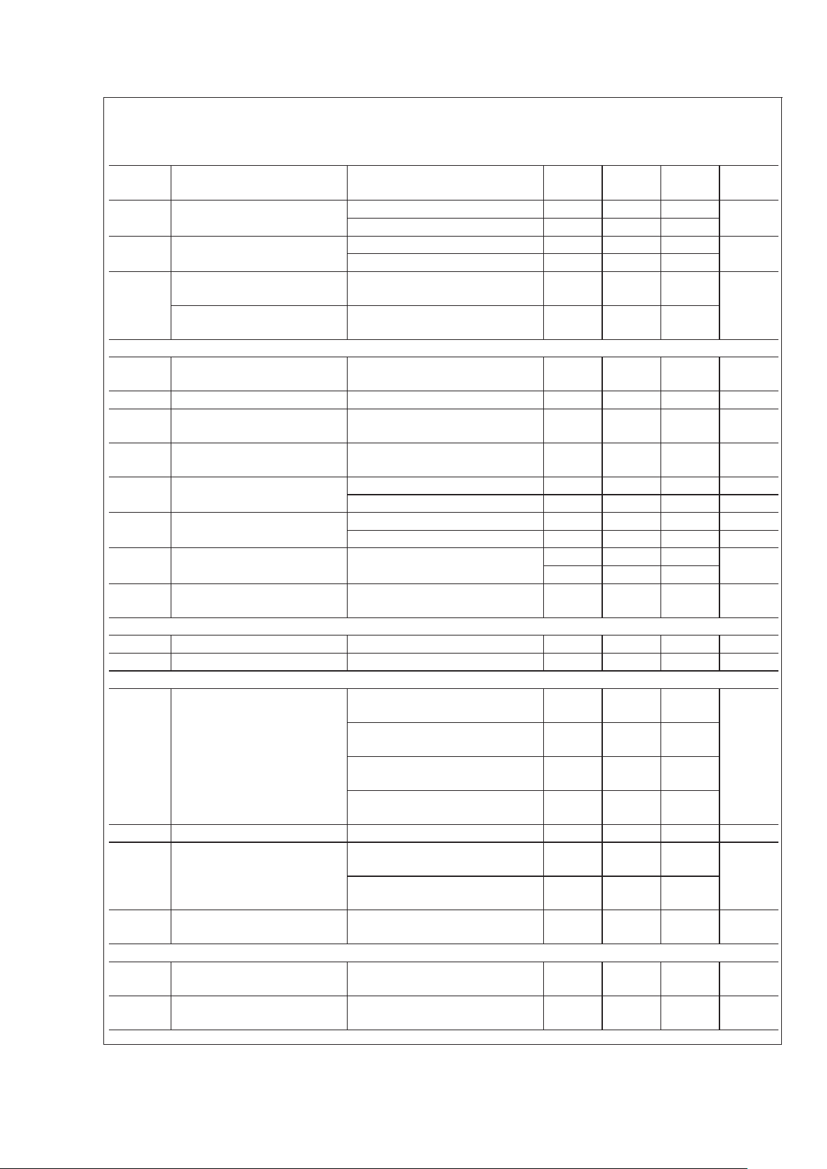
2.5V Electrical Characteristics (Continued)
Unless otherwise specified, all limits guaranteed for TJ= 25˚C, V+= 2.5V, V−= −2.5V, VCM= 0V, AV= +2, RF= 500Ω,
R
L
= 100Ω. Boldface limits apply at the temperature extremes.
Symbol Parameter Conditions Min
(Note 6)
Typ
(Note 5)
Max
(Note 6)
Units
HD2 2
nd
Harmonic Distortion fc = 1MHz, VO=2VPP,RL= 100Ω −88
dBc
fc = 1MHz, V
O
=2VPP,RL= 500Ω −98
HD3 3
rd
Harmonic Distortion fc = 1MHz, VO=2VPP,RL= 100Ω −92
dBc
fc = 1MHz, V
O
=2VPP,RL= 500Ω −100
MTPR Upstream V
O
= 0.4V
RMS
,26kHz to 132kHz
(see test circuit 5)
−76
dBc
Downstream V
O
= 0.4V
RMS
,144kHz to 1.1MHz
(see test circuit 5)
−68
Input Characteristics
V
OS
Input Offset Voltage VCM= 0V −1.5
−2.3
+0.3 +1.5
+2.3
mV
TC V
OS
Input Offset Average Drift VCM= 0V (Note 7) −2.5 µV/˚C
I
OS
Input Offset Current VCM= 0V −1.5
−2.5
+0.01 1.5
2.5
µA
I
B
Input Bias Current VCM= 0V 4.6 10
15
µA
R
IN
Input Resistance Common Mode 17 MΩ
Differential Mode 12 kΩ
C
IN
Input Capacitance Common Mode 0.9 pF
Differential Mode 1.0 pF
CMVR Input Common Mode Voltage
Range
CMRR ≥ 60dB −1.25 −1
V
2 +2.2
CMRR Common Mode Rejection Ratio Input Referred,
V
CM
= −0.7 to +1.7V
80
75
100 dB
Transfer Characteristics
A
VOL
Large Signal Voltage Gain VO=1V
PP
74 82 dB
X
t
Crosstalk f = 1MHz −75 dB
Output Characteristics
V
O
Output Swing No Load, Positive Swing 1.4
1.2
1.7
V
No Load, Negative Swing −1.5 −1.2
−1
R
L
= 100Ω, Positive Swing 1.2
1
1.5
R
L
= 100Ω, Negative Swing −1.4 −1.1
−0.9
R
O
Output Impedance f = 1MHz 0.1 Ω
I
SC
Output Short Circuit Current Sourcing to Ground
∆V
IN
= 200mV (Note 3), (Note 9)
100 137
mA
Sinking to Ground
∆V
IN
= −200mV (Note 3), (Note 9)
100 134
I
OUT
Output Current Sourcing, VO= +0.8V
Sinking, V
O
= −0.8V
90 mA
Power Supply
+PSRR Positive Power Supply Rejection
Ratio
Input Referred,
V
S
= +2.5V to +3V
78
72
93
dB
−PSRR Negative Power Supply
Rejection Ratio
Input Referred,
V
S
= −2.5V to −3V
75
70
88 dB
LMH6622
www.national.com 4

±
2.5V Electrical Characteristics (Continued)
Unless otherwise specified, all limits guaranteed for TJ= 25˚C, V+= 2.5V, V−= −2.5V, VCM= 0V, AV= +2, RF= 500Ω,
R
L
= 100Ω. Boldface limits apply at the temperature extremes.
Symbol Parameter Conditions Min
(Note 6)
Typ
(Note 5)
Max
(Note 6)
Units
I
S
Supply Current (per amplifier) No Load 4.1 5.8
6.4
mA
Note 1: Absolute Maximum Ratings indicate limits beyond which damage to the device may occur. Operating Ratings indicate conditions for which the device is
intended to be functional, but specific performance is not guaranteed. For guaranteed specifications and the test conditions, see the Electrical Characteristics.
Note 2: Human body model, 1.5kΩ in series with 100pF. Machine model, 0Ω in series with 200pF.
Note 3: Applies to both single-supply and split-supply operation. Continuous short circuit operation at elevated ambient temperature can result in exceeding the
maximum allowed junction temperature of 150˚C.
Note 4: The maximum power dissipation is a function of T
J(MAX)
, θJAand TA. The maximum allowable power dissipation at any ambient temperature is PD=
(T
J(MAX)−TA
)/θJA. All numbers apply for packages soldered directly onto a PC board.
Note 5: Typical values represent the most likely parametric norm.
Note 6: All limits are guaranteed by testing or statistical analysis.
Note 7: Offset voltage average drift is determined by dividing the change in V
OS
at temperature extremes into the total temperature change.
Note 8: Slew rate is the slowest of the rising and falling slew rates.
Note 9: Short circuit test is a momentary test.Output short circuitduration is infinitefor V
S
≤±2.5V,atroom temperature andbelow.For V
S
>
±
2.5V,allowableshort
circuit duration is 1.5ms.
LMH6622
www.national.com5
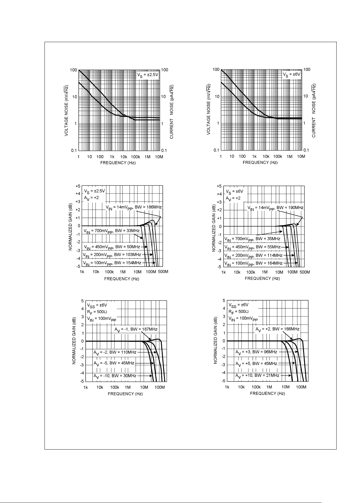
Typical Performance Characteristics
Current and Voltage Noise vs. Frequency Current and Voltage Noise vs. Frequency
20029224
20029225
Frequency Response vs. Input Signal Level Frequency Response vs. Input Signal Level
20029202 20029203
Inverting Amplifier Frequency Response Non-Inverting Amplifier Frequency Response
20029246 20029247
LMH6622
www.national.com 6
 Loading...