

NSC LMH6552, LMH6552MA Datasheet
April 2007
LMH6552
1 GHz Fully Differential Amplifier
General Description
The LMH6552 is a high performance fully differential amplifier
designed to provide the exceptional signal fidelity and wide
large-signal bandwidth necessary for driving 8 to 14 bit high
speed data acquisition systems. Using National's proprietary
differential current mode input stage architecture, the
LMH6552 allows operation at gains greater than unity without
sacrificing response flatness, bandwidth, harmonic distortion,
or output noise performance.
With external gain set resistors and integrated common mode
feedback, the LMH6552 can be configured as either a differential input to differential output or single ended input to
differential output gain block. The LMH6552 can be AC or DC
coupled at the input which makes it suitable for a wide range
of applications including communication systems and high
speed oscilloscope front ends. The LMH6552 is available in
an 8-pin SOIC package as well as a space saving, thermally
enhanced 8-pin LLP package for higher performance.
Features
■
1.0 GHz bandwidth @ AV = 1
■
800 MHz bandwidth @ AV = 4
■
450 MHz 0.1 dB flatness
■
3800 V/µs slew rate
■
10 ns settling time to 0.1%
■
−90 dB THD @ 20 MHz
■
−74 dB THD @ 70 MHz
■
20 ns enable/shutdown pin
■
5 to 12V operation
Applications
■
Differential ADC driver
■
Video over twisted pair
■
Differential line driver
■
Single end to differential converter
■
High speed differential signaling
■
IF/RF amplifier
■
SAW filter buffer/driver
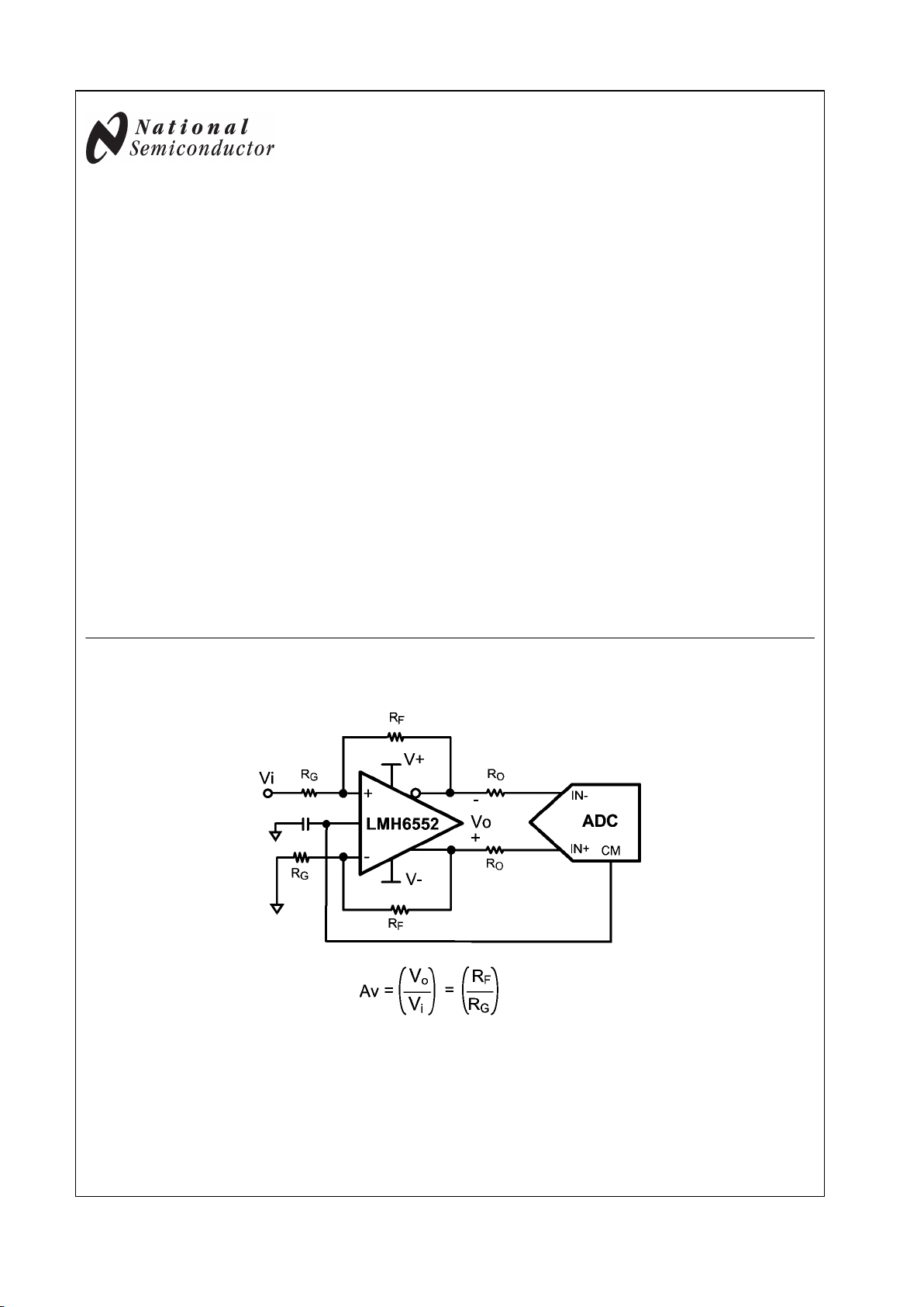
Typical Application
Single-Ended Input Differential Output
30003544
LMH™ is a trademark of National Semiconductor Corporation.
© 2007 National Semiconductor Corporation 300035 www.national.com
LMH6552 1 GHz Fully Differential Amplifier
Absolute Maximum Ratings (Note 1)
If Military/Aerospace specified devices are required,
please contact the National Semiconductor Sales Office/
Distributors for availability and specifications.
ESD Tolerance (Note 6)
Human Body Model 2000V
Machine Model 200V
Supply Voltage 13.2V
Common Mode Input Voltage ±V
S
Maximum Input Current (pins 1, 2, 7, 8) 30 mA
Maximum Output Current (pins 4, 5) (Note 4)
Soldering Information
Infrared or Convection (20 sec) 235°C
Wave Soldering (10 sec) 260°C
Operating Ratings (Note 1)
Operating Temperature Range
(Note 3) −40°C to +85°C
Storage Temperature Range −65°C to +150°C
Total Supply Voltage 4.5V to 12V
Package Thermal Resistance (θJA) (Note 5)
8-Pin SOIC 150°C/W
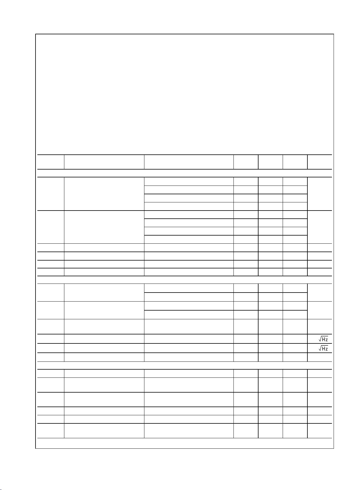
±5V Electrical Characteristics (Note 2)
Unless otherwise specified, all limits are guaranteed for TA = 25°C, V+ = +5V, V− = −5V, AV= 1, VCM = 0V, RF = RG = 357Ω,
RL = 500Ω, for single ended in, differential out. Boldface limits apply at the temperature extremes.
Symbol Parameter Conditions Min
(Note 8)
Typ
(Note 7)
Max
(Note 8)
Units
AC Performance (Differential)
SSBW Small Signal −3 dB Bandwidth
(Note 8)
V
OUT
= 0.2 VPP, AV = 1 1000
MHz
V
OUT
= 0.2 VPP, AV = 2 930
V
OUT
= 0.2 VPP, AV = 4 810
V
OUT
= 0.2 VPP, AV = 8 590
LSBW Large Signal −3 dB Bandwidth V
OUT
= 2 VPP, AV = 1 950
MHz
V
OUT
= 2 VPP, AV = 2 820
V
OUT
= 2 VPP, AV = 4 740
V
OUT
= 2 VPP, AV = 8 590
0.1 dB Bandwidth V
OUT
= 0.2 VPP, AV = 1 450 MHz
Slew Rate 4V Step, AV = 1 3800
V/μs
Rise/Fall Time, 10%-90% 2V Step 750 ps
0.1% Settling Time 2V Step 10 ns
Distortion and Noise Response
HD2 2nd Harmonic Distortion
V
OUT
= 2 VPP, f = 20 MHz, RL = 800Ω
−92
dBc
V
OUT
= 2 VPP, f = 70 MHz, RL = 800Ω
−74
HD3 3rd Harmonic Distortion
V
OUT
= 2 VPP, f = 20 MHz, RL = 800Ω
−93
dBc
V
OUT
= 2 VPP, f = 70 MHz, RL = 800Ω
−84
IMD3 Two-Tone Intermodulation Freq >70 MHz, Third Order Products,
V
OUT
= 2 VPP Composite
−87 dBc
Input Noise Voltage
f ≥ 1 MHz
1.1
nV/
Input Noise Current
f ≥ 1 MHz
19.5
pA/
Noise Figure (See Figure 5)
50Ω System, AV = 9, 10 MHz
10.3 dB
Input Characteristics
I
BI
Input Bias Current (Note 10) 60 110 µA
I
Boffset
Input Bias Current Differential
(Note 7)
VCM = 0V, VID = 0V, I
Boffset
= (I
B
−
- I
B
+
)/2 2.47 18 µA
CMRR Common Mode Rejection Ratio
(Note 7)
DC, VCM = 0V, VID = 0V 80 dBc
R
IN
Input Resistance Differential 15
Ω
C
IN
Input Capacitance Differential 0.5 pF
CMVR Input Common Mode Voltage
Range
CMRR > 38 dB ±3.5 ±3.8 V
www.national.com 2
LMH6552
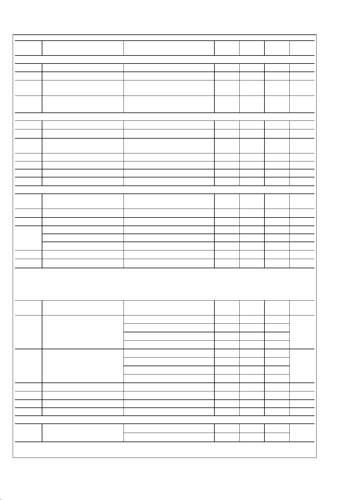
Symbol Parameter Conditions Min
(Note 8)
Typ
(Note 7)
Max
(Note 8)
Units
Output Performance
Output Voltage Swing (Note 7) Differential Output 14.8 15.4 V
PP
I
OUT
Linear Output Current (Note 7) V
OUT
= 0V ±70 ±80 mA
I
SC
Short Circuit Current One Output Shorted to Ground VIN = 2V
Single Ended (Note 6)
±141 mA
Output Balance Error
ΔV
OUT
Common Mode /ΔV
OUT
Differential , ΔVOD = 1V, f < 1 MHz
-60 dB
Miscellaneous Performance
Z
T
Open Loop Transimpedance Differential 108
dBΩ
PSRR Power Supply Rejection Ratio
DC, ΔVS = ±1V
80 dB
I
S
Supply Current (Note 7)
RL = ∞
19 22.5 25
28
mA
Enable Voltage Threshold 3.0 V
Disable Voltage Threshold 2.0 V
Enable/Disable time 15 ns
I
SD
Disable Shutdown Current 500 600
μA
Output Common Mode Control Circuit
Common Mode Small Signal
Bandwidth
V
IN
+
= V
IN
−
= 0 400 MHz
Slew Rate V
IN
+
= V
IN
−
= 0 607
V/μs
V
OSCM
Input Offset Voltage Common Mode, VID = 0, VCM = 0 1.5 ±16.5 mV
Input Bias Current (Note 9) −3.2 ±8 µA
Voltage Range ±3.7 ±3.8 V
CMRR Measure VOD, VID = 0V 80 dB
Input Resistance 200
kΩ
Gain
ΔV
O,CM
/ΔV
CM
0.995 1.0 1.012 V/V
±2.5V Electrical Characteristics (Note 2)
Unless otherwise specified, all limits are guaranteed for TA = 25°C, V+ = +2.5V, V− = −2.5V, AV = 1, VCM = 0V, RF = RG = 357Ω,
RL = 500Ω, for single ended in, differential out. Boldface limits apply at the temperature extremes.
Symbol Parameter Conditions Min
(Note 8)
Typ
(Note 7)
Max
(Note 8)
Units
SSBW Small Signal −3 dB Bandwidth
(Note 8)
V
OUT
= 0.2 VPP, AV = 1 800
MHz
V
OUT
= 0.2 VPP, AV = 2 740
V
OUT
= 0.2 VPP, AV = 4 660
V
OUT
= 0.2 VPP, AV = 8 498
LSBW Large Signal −3 dB Bandwidth V
OUT
= 2 VPP, AV = 1 690
MHz
V
OUT
= 2 VPP, AV = 2 620
V
OUT
= 2 VPP, AV = 4 589
V
OUT
= 2 VPP, AV = 8 480
0.1 dB Bandwidth V
OUT
= 0.2 VPP, AV = 1 300 MHz
Slew Rate 2V Step, AV = 1 2100
V/μs
Rise/Fall Time, 10% to 90% 2V Step 1.2 ns
0.1% Settling Time 2V Step 10 ns
Distortion and Noise Response
HD2 2nd Harmonic Distortion
V
OUT
= 2 VPP, f = 20 MHz, RL = 800Ω
82
dBc
V
OUT
= 2 VPP, f = 70 MHz, RL = 800Ω
65
3 www.national.com
LMH6552
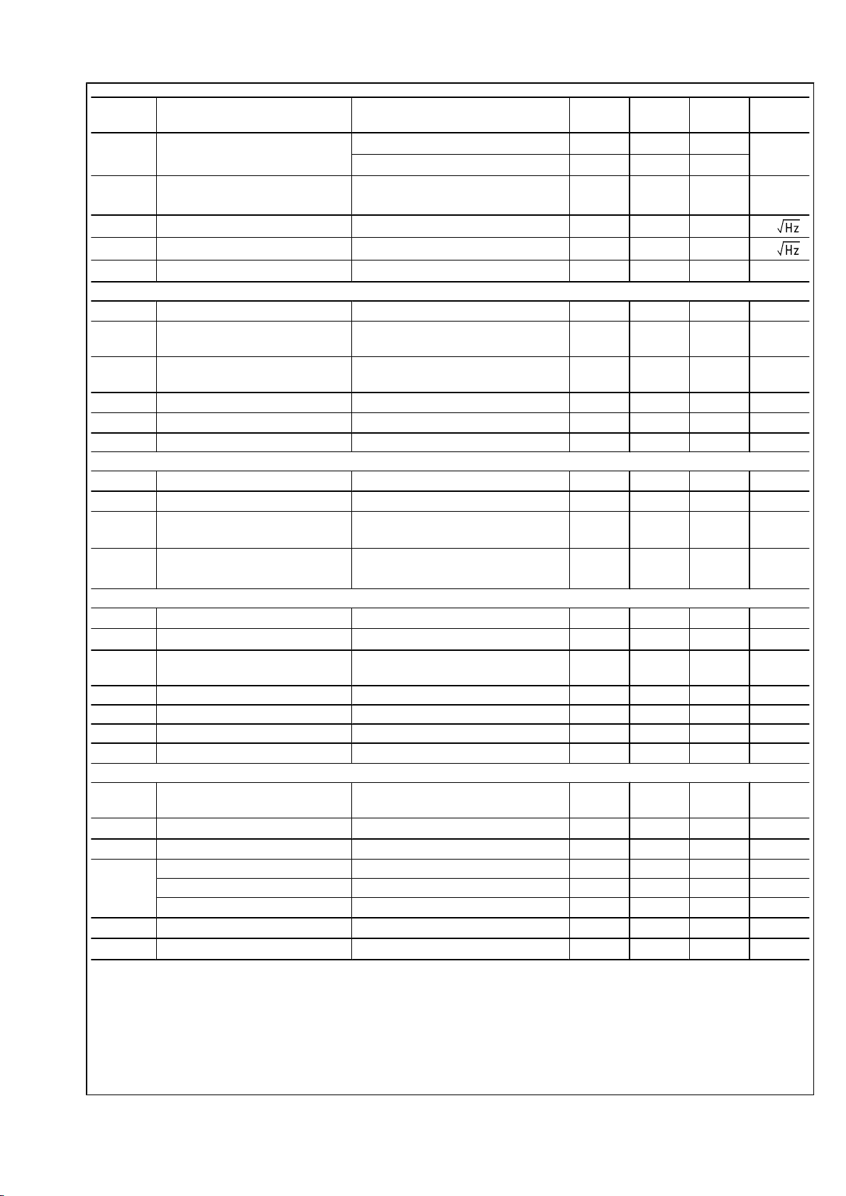
Symbol Parameter Conditions Min
(Note 8)
Typ
(Note 7)
Max
(Note 8)
Units
HD3 3rd Harmonic Distortion
V
OUT
= 2 VPP, f = 20 MHz, RL = 800Ω
79
dBc
V
OUT
= 2 VPP, f = 70 MHz, RL = 800Ω
67
IMD3 Two-Tone Intermodulation
f ≥ 70 MHz, Third Order Products,
V
OUT
= 2 VPP Composite
−77 dBc
Input Noise Voltage
f ≥ 1 MHz
1.1
nV/
Input Noise Current
f ≥ 1 MHz
19.5
pA/
Noise Figure (See Figure 5)
50Ω System, AV = 9, 10 MHz
10.2 dB
Input Characteristics
I
BI
Input Bias Current (Note 10) 54 90 µA
I
Boffset
Input Bias Current Differential
(Note 7)
VCM = 0V, VID = 0V, I
Boffset
= (I
B
−
- I
B
+
)/2 2.3 18
μA
CMRR Common-Mode Rejection Ratio
(Note 7)
DC, VCM = 0V, VID = 0V 75 dBc
R
IN
Input Resistance Differential 15
Ω
C
IN
Input Capacitance Differential 0.5 pF
CMVR Input Common Mode Range CMRR > 38 dB 1.5-3.5 1.2-3.8 V
Output Performance
Output Voltage Swing (Note 7) Differential Output 5.6 6.0 V
PP
I
OUT
Linear Output Current (Note 7) V
OUT
= 0V ±55 ±65 mA
I
SC
Short Circuit Current One Output Shorted to Ground, VIN = 2V
Single Ended (Note 6)
±131 mA
Output Balance Error
ΔV
OUT
Common Mode /ΔV
OUT
Differential , ΔVOD = 1V, f < 1 MHz
60 dB
Miscellaneous Performance
ZT Open Loop Transimpedance Differential 107
dBΩ
PSRR Power Supply Rejection Ratio
DC, ΔVS = ±1V
80 dB
I
S
Supply Current (Note 7)
RL = ∞
17 20.4 24
27
mA
Enable Voltage Threshold 3.0 V
Disable Voltage Threshold 2.0 V
Enable/Disable time 15 ns
I
SD
Disable Shutdown Current 500 600 µA
Output Common Mode Control Circuit
Common Mode Small Signal
Bandwidth
V
IN
+
= V
IN
−
= 0 310 MHz
Slew Rate V
IN
+
= V
IN
−
= 0 430
V/μs
V
OSCM
Input Offset Voltage Common Mode, VID = 0, VCM = 0 1.65 ±15 mV
Input Bias Current (Note 9) −2.9 µA
Voltage Range ±1.19 ±1.25 V
CMRR Measure VOD, VID = 0V 80 dB
Input Resistance 200
kΩ
Gain
ΔV
O,CM
/ΔV
CM
0.995 1.0 1.012 V/V
www.national.com 4
LMH6552
Note 1: Absolute Maximum Ratings indicate limits beyond which damage to the device may occur. Operating Ratings indicate conditions for which the device is
intended to be functional, but specific performance is not guaranteed. For guaranteed specifications, see the Electrical Characteristics tables.
Note 2: Electrical Table values apply only for factory testing conditions at the temperature indicated. Factory testing conditions result in very limited self-heating
of the device such that TJ = TA. No guarantee of parametric performance is indicated in the electrical tables under conditions of internal self-heating where
TJ > TA. See Applications Section for information on temperature de-rating of this device." Min/Max ratings are based on product characterization and simulation.
Individual parameters are tested as noted.
Note 3: The maximum power dissipation is a function of T
J(MAX)
, θJA. The maximum allowable power dissipation at any ambient temperature is
PD = (T
J(MAX)
– TA) / θJA. All numbers apply for packages soldered directly onto a PC Board.
Note 4: The maximum output current (I
OUT
) is determined by device power dissipation limitations. See the Power Dissipation section of the Application Section
for more details.
Note 5: Human Body Model, applicable std. MIL-STD-883, Method 30157. Machine Model, applicable std. JESD22-A115-A (ESD MM std. of JEDEC). FieldInduced Charge-Device Model, applicable std. JESD22-C101-C (ESD FICDM std. of JEDEC).
Note 6: Short circuit current should be limited in duration to no more than 10 seconds. See the Power Dissipation section of the Application Information for more
details.
Note 7: Typical values represent the most likely parametric norm as determined at the time of characterization. Actual typical values may vary over time and will
also depend on the application and configuration. The typical values are not tested and are not guaranteed on shipped production material.
Note 8: Limits are 100% production tested at 25°C. Limits over the operating temperature range are guaranteed through correlation using Statistical Quality
Control (SQC) methods.
Note 9: Negative input current implies current flowing out of the device.
Note 10: IBI is referred to a differential output offset voltage by the following relationship: V
OD(offset)
= IBI*2R
F
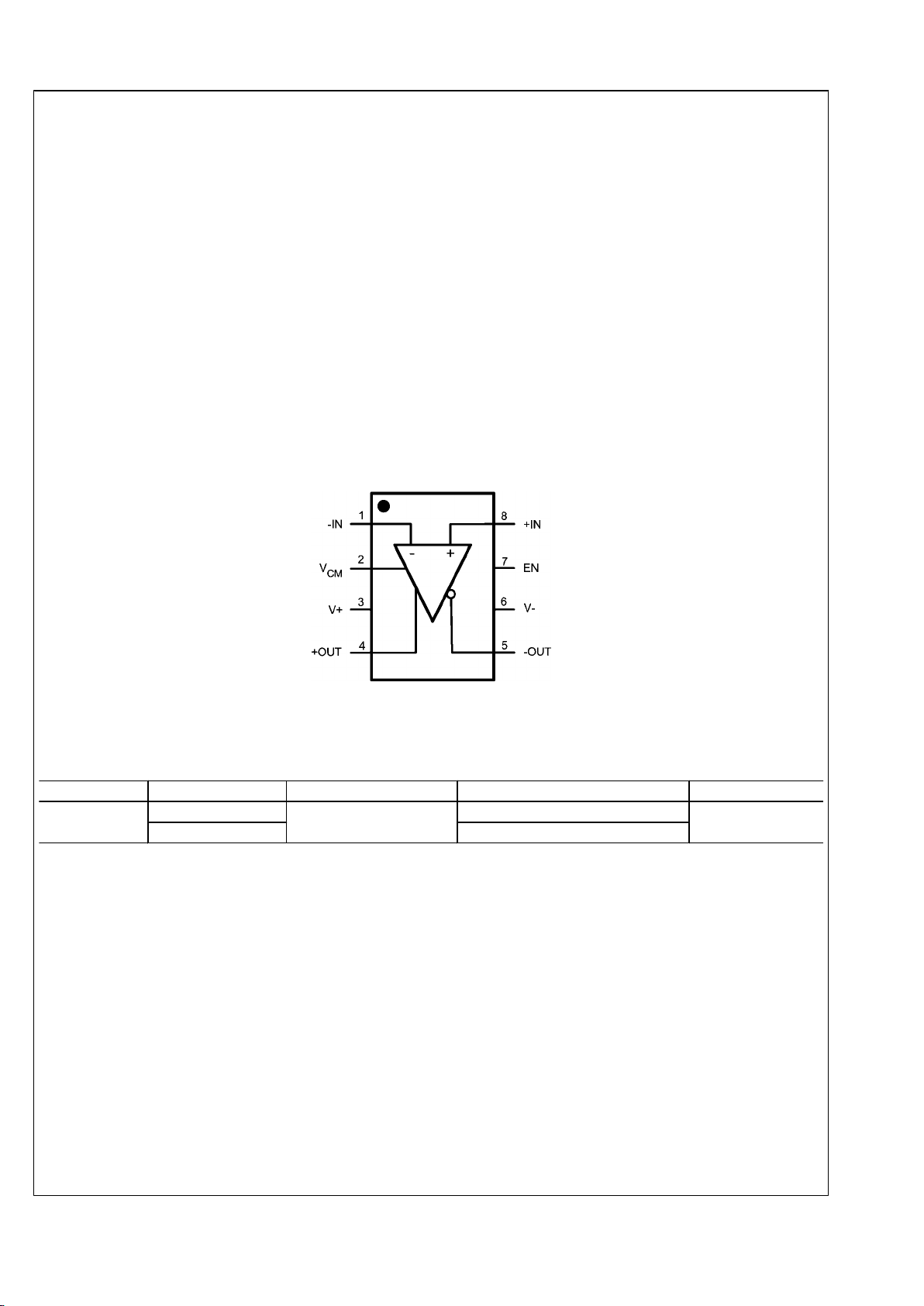
Connection Diagram
8-Pin SOIC
30003508
Top View
Ordering Information
Package Part Number Package Marking Transport Media NSC Drawing
8-Pin SOIC
LMH6552MA
LMH6552MA
95/Rails
M08A
LMH6552MAX 2.5k Units Tape and Reel
5 www.national.com
LMH6552
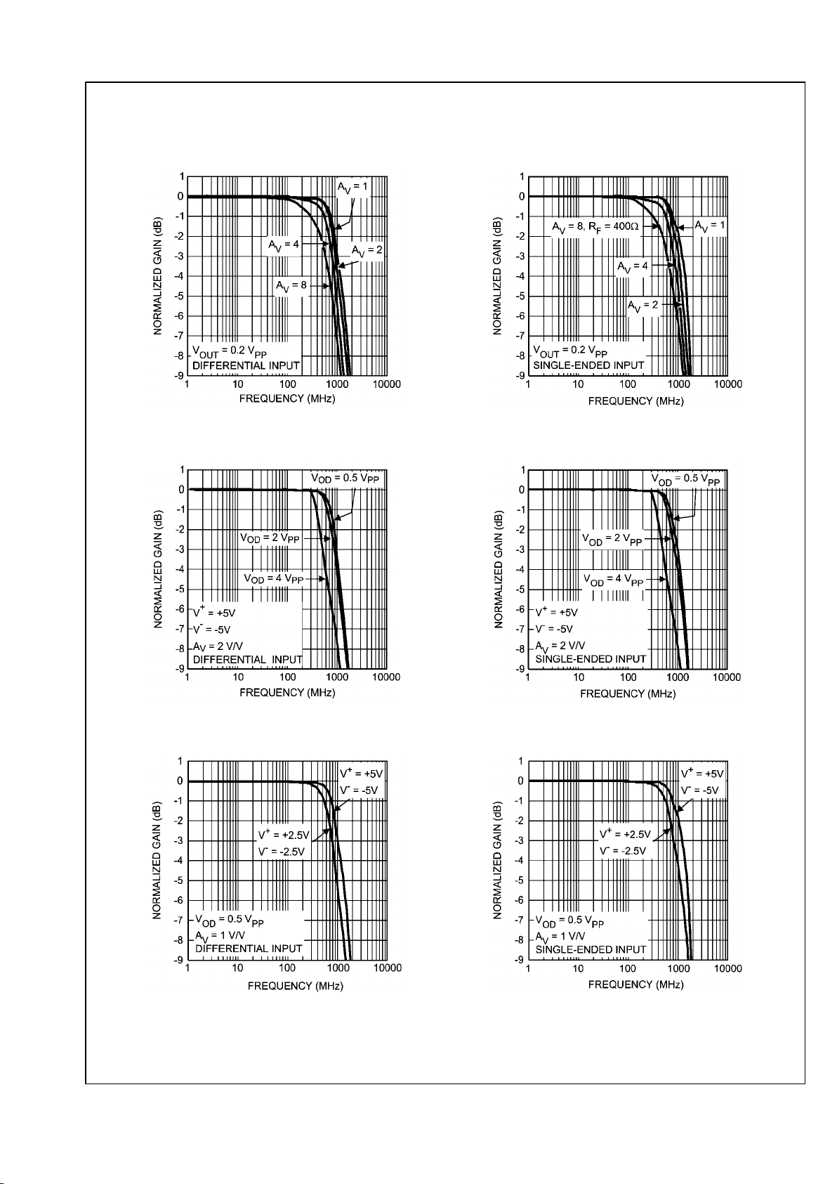
Typical Performance Characteristics V+ = +5V, V− = −5V (T
A
= 25°C, RF = RG =
357Ω, RL = 500Ω, AV = 1, for single ended in, differential out, unless specified).
Frequency Response vs. Gain
30003547
Frequency Response vs. Gain
30003534
Frequency Response vs. V
OUT
30003548
Frequency Response vs. V
OUT
30003516
Frequency Response vs. Supply Voltage
30003514
Frequency Response vs. Supply Voltage
30003515
www.national.com 6
LMH6552
 Loading...