October 2007
LMH6515
600 MHz, Digital Controlled, Variable Gain Amplifier
General Description
The LMH6515 is a high performance, digitally controlled variable gain amplifier (DVGA). It combines precision gain control
with a low noise, ultra-linear, differential amplifier. Typically,
the LMH6515 drives a high performance ADC in a broad
range of mixed signal and digital communication applications
such as mobile radio and cellular base stations where automatic gain control (AGC) is required to increase system dynamic range. When used in conjunction with a high speed
ADC, system dynamic range can be extended by up to 32 dB.
The LMH6515 has a differential input and output allowing
large signal swings on a single 5V supply. It is designed to
accept signals from RF elements and maintain a terminated
impedance environment. The input impedance is 200Ω resistive. The output impedance is either 200Ω or 400Ω and is
user selectable. A unique internal architecture allows use with
both single ended and differential input signals.
Input signals to the LMH6515 are scaled by a highly linear,
digitally controlled attenuator with 31 accurate 1 dB steps.
The attenuator output provides the input signal for a high gain,
ultra linear differential transconductor. The transconductor
differential output current can be converted into a voltage by
using the on-chip 200Ω or 400Ω loads. The transconductance
gain is 0.1 Amp/Volt resulting in a maximum voltage gain of
+26 dB when driving a 200Ω load, or 32 dB when driving the
400Ω load. On chip digital latches are provided for local storage of the gain setting. The gain step settling time is 5 ns and
care has been taken to reduce the sensitivity of bandwidth
and phase to gain setting.
The LMH6515 operates over the industrial temperature range
of −40°C to +85°C. The LMH6515 is available in a 16-Pin,
thermally enhanced, LLP package.
Features
■
Adjustable gain with a 31 dB range
■
Precise 1 dB gain steps
■
Parallel 5-bit gain control
■
On chip register stores gain setting
■
Fully differential signal path
■
Single ended to differential capable
■
200Ω input impedance
■
Small footprint (4 mm x 4 mm) LLP package
Key Specifications
■
600 MHz bandwidth @ 100Ω load
■
40 dBm OIP3 @ 75 MHz, 200Ω load
■
20 dB to 30 dB maximum gain
■
Selectable output impedance of 200Ω or 400Ω
■
8.3 dB noise figure
■
5 ns gain step switching time
■
100 mA supply current
Applications
■
Cellular base stations
■
IF sampling receivers
■
Instrumentation
■
Modems
■
Imaging
■
Differential line receiver
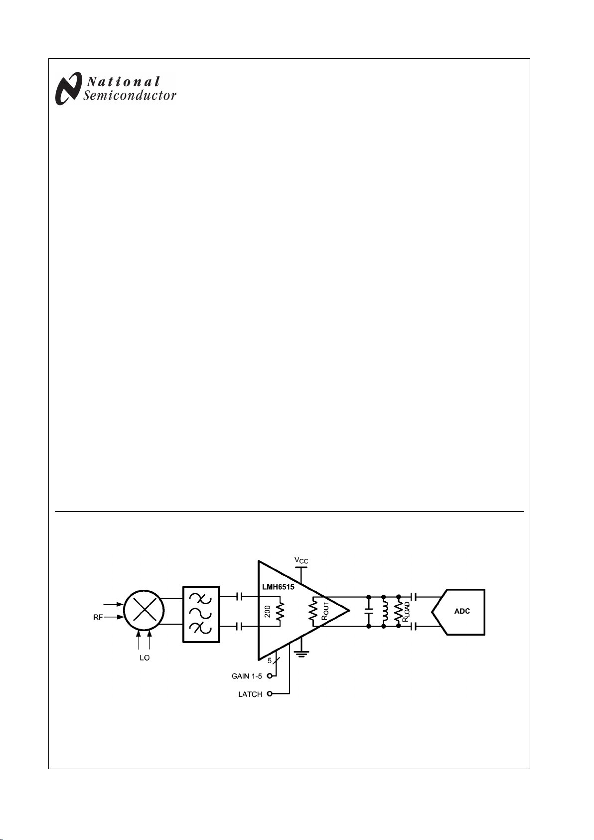
Typical Application
20214301
LMH™ is a trademark of National Semiconductor Corporation.
© 2007 National Semiconductor Corporation 202143 www.national.com
LMH6515 600 MHz, Digital Controlled, Variable Gain Amplifier

Absolute Maximum Ratings (Note 1)
If Military/Aerospace specified devices are required,
please contact the National Semiconductor Sales Office/
Distributors for availability and specifications.
ESD Tolerance (Note 2)
Human Body Model 2 kV
Machine Model 150V
Positive Supply Voltage (Pin 3) −0.6V to 5.5V
Output Voltage (pin 14,15) −0.6V to 6.8V
Differential Voltage Between Any
Two Grounds <200 mV
Analog Input Voltage Range −0.6V to V
CC
Digital Input Voltage Range −0.6V to 3.6V
Output Short Circuit Duration
(one pin to ground) Infinite
Junction Temperature +150°C
Storage Temperature Range −65°C to +150°C
Soldering Information
Infrared or Convection (20 sec) 235°C
Wave Soldering (10 sec) 260°C
Operating Ratings (Note 1)
Supply Voltage (Pin 3) 4V to 5.25V
Output Voltage Range (Pin 14, 15) 1.4V to 6.4V
Differential Voltage Between Any
Two Grounds <10 mV
Analog Input Voltage Range,
AC Coupled ±1.4V
Temperature Range (Note 3) −40°C to +85°C
Package Thermal Resistance (θJA)
16-Pin LLP 47°C/W
5V Electrical Characteristics (Note 4)
The following specifications apply for single supply with VCC = 5V, Maximum Gain , RL = 100Ω (200Ω external || 200Ω internal),
V
OUT
= 2 VPP, fin = 150 MHz. Boldface limits apply at temperature extremes.
Symbol Parameter Conditions Min
(Note 6)
Typ
(Note 5)
Max
(Note 6)
Units
Dynamic Performance
SSBW −3 dB Bandwidth Average of all Gain Settings 600 MHz
Noise and Distortion
Third Order Intermodulation
Products
f = 75 MHz, V
OUT
= 2 V
PP
−76
dBc
f = 150 MHz, V
OUT
= 2 V
PP
−72
f = 250 MHz, V
OUT
= 2 V
PP
−66
f = 450 MHz, V
OUT
= 2 V
PP
−58
OIP3 Output 3rd Order Intercept Point f = 75 MHz, V
OUT
= 2 VPP,
Tone Spacing = 0.5 MHz
39
dBm
f = 150 MHz, V
OUT
= 2 VPP,
Tone Spacing = 2 MHz
37
f = 250 MHz, V
OUT
= 2 VPP,
Tone Spacing = 2 MHz
34
f = 75 MHz, RL = 200Ω, V
OUT
= 2 VPP,
Tone Spacing = 0.5 MHz
40
f = 150 MHz, RL = 200Ω, V
OUT
= 2 VPP,
Tone Spacing = 2 MHz
37
f = 250 MHz, RL = 200Ω, V
OUT
= 2 VPP,
Tone Spacing = 2 MHz
34
P1 dB Output Level for 1 dB Gain
Compression
f = 75 MHz, RL = 200Ω
16.7
dBm
f = 250 MHz, RL = 200Ω
14.7
f = 75 MHz 14.5
f = 450 MHz 13.2
VNI Input Noise Voltage Maximum Gain, f = 40 MHz 1.8
nV/
VNO Output Noise Voltage Maximum Gain, f = 40 MHz 18
nV/
NF Noise Figure Maximum Gain 8.3 dB
Analog I/O
Differential Input Resistance 165
160
186 210
220
Ω
Input Common Mode Resistance 825
785
971 1120
1160
Ω
www.national.com 2
LMH6515

Symbol Parameter Conditions Min
(Note 6)
Typ
(Note 5)
Max
(Note 6)
Units
Differential Output Impedance Low Gain Option 187
Ω
High Gain Option 330
325
370 410
415
Internal Load Resistors Between Pins 13, 14 and Pins 15, 16 165
160
187 210
235
Ω
Input Signal Level (AC Coupled)
Max Gain, VO = 2 VPP, RL = 1 kΩ
126 mV
PP
Maximum Differential Input Signal AC Coupled 5.6 V
PP
Input Common Mode Voltage Self Biased 1.3
1.1
1.4 1.5
1.7
V
Input Common Mode Voltage
Range
Driven Externally 0.9 to 2.0 V
Minimum Input Voltage DC 0 V
Maximum Input Voltage DC 3.3 V
Maximum Differential Output
Voltage Swing
VCC = 5V, Output Common Mode = 5V 5.5 V
PP
V
OS
Output Offset Voltage All Gain Settings 30 mV
CMRR Common Mode Rejection Ratio 85 dB
PSRR Power Supply Rejection Ratio 63
61
83
dB
Gain Parameters
Maximum Gain
DC, Internal RL = 200Ω,
External RL = 1280Ω
23.9
23.4
24.2 24.6
24.8
dB
Minimum Gain
DC, Internal RL = 200Ω,
External RL = 1280Ω
−7.2
−7.7
−6.9 −6.5
−6.4
dB
Gain Step Size DC 1.0 dB
Gain Step Error DC 0.02
dB
f = 150 MHz 0.07
Cumulative Gain Step Error DC, Gain Step 31 to Gain Step 0 −0.1
−0.2
0.05 0.3
0.4
dB
Gain Step Switching Time 5 ns
Digital Inputs/Timing
Logic Compatibility CMOS Logic 3.3 V
VIL Logic Input Low Voltage 0.8 V
VIH Logic Input High Voltage 2.0 V
IIH Logic Input High Input Current 32 40
μA
TSU Setup Time 3 ns
THOLD Hold Time 3 ns
TPW Minimum Latch Pulse Width 10 ns
Power Requirements
ICC Total Supply Current V
OUT
= 0V Differential, V
OUT
Common
Mode = 5V
107 124
134
mA
Amplifier Supply Current Pin 3 Only 56 66
74
mA
Output Stage Bias Currents Pins 13, 14 and Pins 15, 16;
V
OUT
Common Mode = 5 V
48 58
60
mA
3 www.national.com
LMH6515

Note 1: Absolute Maximum Ratings indicate limits beyond which damage to the device may occur. Operating Ratings indicate conditions for which the device is
intended to be functional, but specific performance is not guaranteed. For guaranteed specifications, see the Electrical Characteristics tables.
Note 2: Human Body Model, applicable std. MIL-STD-883, Method 3015.7. Machine Model, applicable std. JESD22-A115-A (ESD MM std. of JEDEC)
Field-Induced Charge-Device Model, applicable std. JESD22-C101-C (ESD FICDM std. of JEDEC).
Note 3: The maximum power dissipation is a function of T
J(MAX)
, θJA. The maximum allowable power dissipation at any ambient temperature is
PD = (T
J(MAX)
– TA)/ θJA. All numbers apply for packages soldered directly onto a PC Board.
Note 4: Electrical Table values apply only for factory testing conditions at the temperature indicated. No guarantee of parametric performance is indicated in the
electrical tables under conditions different than those tested
Note 5: Typical values represent the most likely parametric norm as determined at the time of characterization. Actual typical values may vary over time and will
also depend on the application and configuration. The typical values are not tested and are not guaranteed on shipped production material.
Note 6: Limits are 100% production tested at 25°C. Limits over the operating temperature range are guaranteed through correlation using Statistical Quality
Control (SQC) methods.
Note 7: Negative input current implies current flowing out of the device.
Note 8: Drift determined by dividing the change in parameter at temperature extremes by the total temperature change.
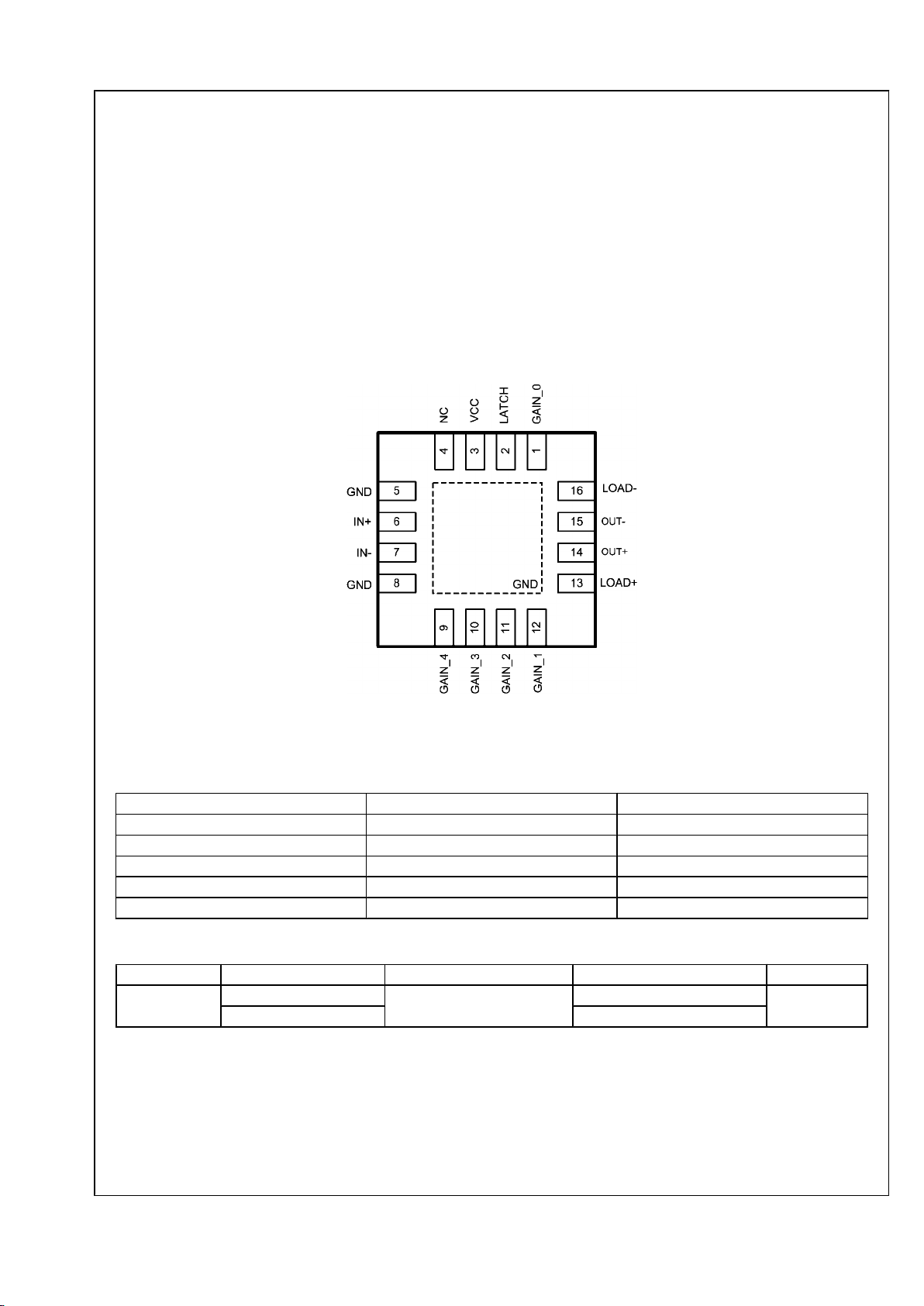
Connection Diagram
16-Pin LLP
20214304
Top View
Gain Control Pins
Pin Number Pin Name Gain Step Size
1 GAIN_0 1 dB
12 GAIN_1 2 dB
11 GAIN_2 4 dB
10 GAIN_3 8 dB
9 GAIN_4 16 dB
Ordering Information
Package Part Number Package Marking Transport Media NSC Drawing
16-Pin LLP
LMH6515SQ
L6515SQ
1k Units Tape and Reel
SQA16A
LMH6515SQX 4.5k Units Tape and Reel
www.national.com 4
LMH6515

Pin Descriptions
Pin Number Symbol Description
Analog I/O
6 IN+ Non-inverting analog input. Internally biased to 1.4V. Input voltage should not exceed
VCC or go below GND by more than 0.5V.
7 IN− Inverting analog input. Internally biased to 1.4V. Input voltage should not exceed VCC or
go below GND by more than 0.5V. If using amplifier single ended this input should be
capacitively coupled to ground.
15 OUT− Open collector inverting output. This pin is an output that also requires a power source.
This pin should be connected to 5V through either an RF choke or an appropriately sized
inductor that can form part of a filter. See application section for details.
14 OUT+ Open collector non-inverting output. This pin is an output that also requires a power
source. This pin should be connected to 5V through either an RF choke or an
appropriately sized inductor that can form part of a filter. See application section for
details.
16 LOAD−
Internal 200Ω resistor connection to pin 15. This pin can be left floating for higher gain
or shorted to pin 13 for lower gain and lower effective output impedance. See application
section for details.
13 LOAD+
Internal 200Ω resistor connection to pin 14. This pin can be left floating for higher gain
or shorted to pin 16 for lower gain and lower effective output impedance. See application
section for details.
Power
3 V
CC
5V power supply pin. Use ceramic, low ESR bypass capacitors. This pin powers
everything except the output stage.
5,8 GND Ground pins. Connect to low impedance ground plane. All pin voltages are specified with
respect to the voltage on these pins. The exposed thermal pad is also a ground
connection.
Digital Inputs
1,12,11,
10,9
GAIN_0 to
GAIN_4
Gain setting pins. See above table for gain step sizes for each pin. These pins are 3.3V
CMOS logic compatible. 5V inputs may cause damage.
2 LATCH This pin controls the function of the gain setting pins mentioned above. With LATCH in
the logic HIGH state the gain is fixed and will not change. With the LATCH in the logic
LOW state the gain is set by the state of the gain control pins. Any changes in gain made
with the LATCH pin in the LOW state will take effect immediately. This pin is 3.3V CMOS
logic compatible. 5V inputs may cause damage.
4 NC This pin is not connected. It can be grounded or left floating.
5 www.national.com
LMH6515

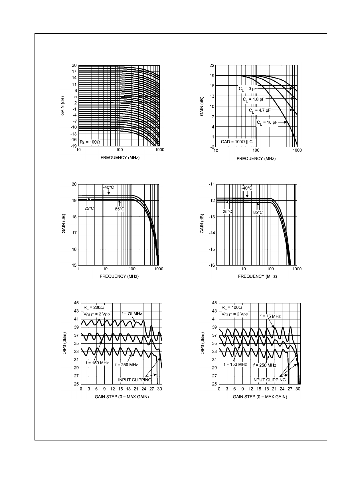
Typical Performance Characteristics V
CC
= 5V
Frequency Response All Gain Settings
20214322
Frequency Response with Capacitive Load
20214325
Frequency Response Over Temperature, Maximum Gain
20214349
Frequency Response Over Temperature, Minimum Gain
20214350
OIP3 High Gain Mode
20214343
OIP3 Low Gain Mode
20214342
www.national.com 6
LMH6515
 Loading...