

LMC6035/LMC6036
Low Power 2.7V Single Supply CMOS Operational
Amplifiers
LMC6035/LMC6036 Low Power 2.7V Single Supply CMOS Operational Amplifiers
January 2000
General Description
The LMC6035/6 is an economical, low voltage op amp capable of rail-to-rail output swing into loads of 600Ω.
LMC6035 is available in a chip sized package (8-Bump micro SMD) using National’s micro SMD package technology.
Both allow for single supply operation and are guaranteed
for 2.7V, 3V, 5V and15Vsupply voltage. The 2.7 supply voltage corresponds to the End-of-Life voltage (0.9V/cell) for
three NiCd or NiMH batteries in series, making the
LMC6035/6 well suited for portable and rechargeable systems. It also features a well behaved decrease in its specifications at supply voltages below its guaranteed 2.7V operation. This provides a “comfort zone” for adequate operation
at voltages significantly below 2.7V. Its ultra low input currents (I
plication, because it allows the use of higher resistor values
and lower capacitor values. In addition, the drive capability of
the LMC6035/6 gives these op amps a broad range of applications for low voltage systems.
) makes it well suited for low power active filter ap-
IN
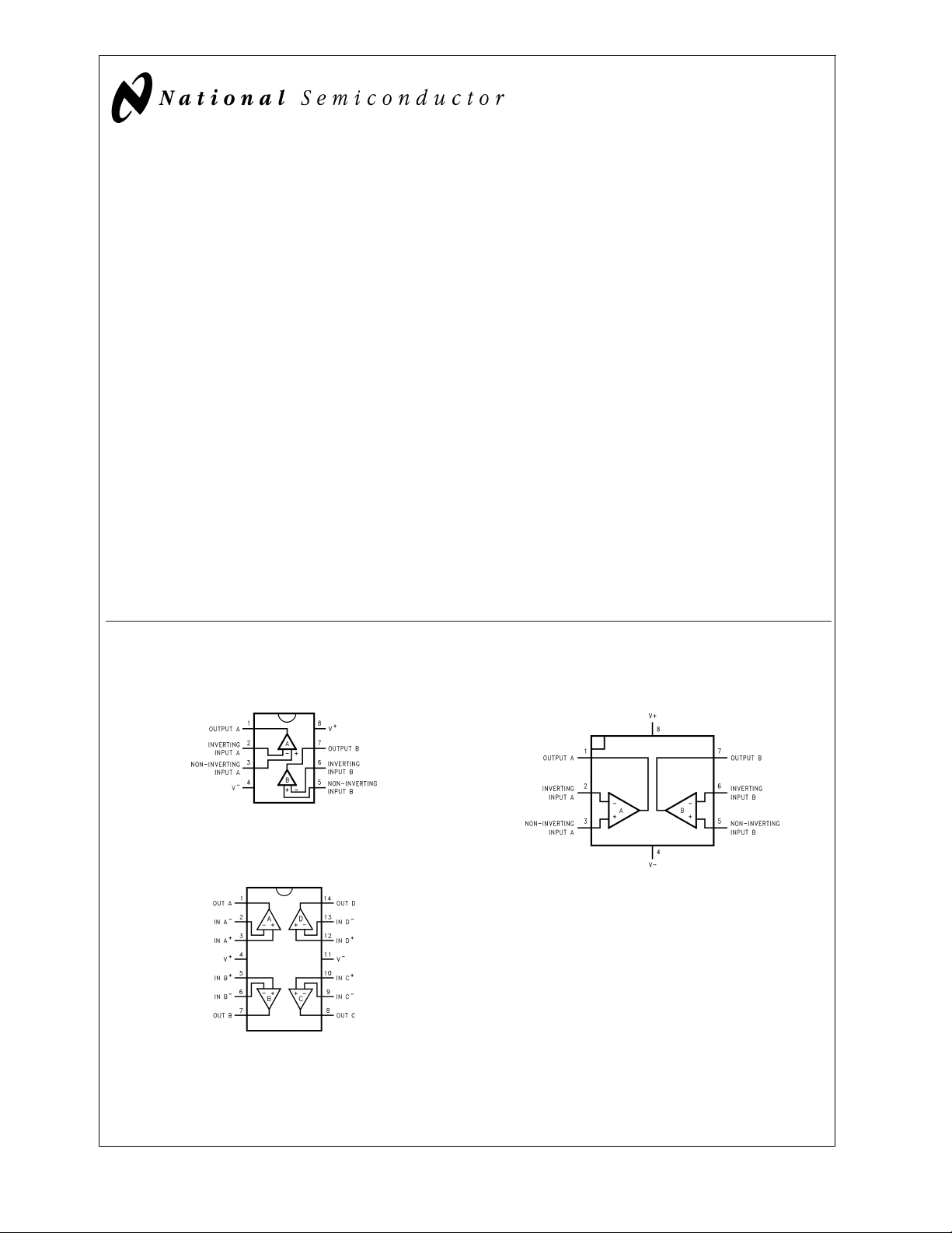
Connection Diagrams
8-Pin SO/MSOP
Features
(Typical Unless Otherwise Noted)
n LMC6035 in micro SMD Package
n Guaranteed 2.7V, 3V, 5V and 15V Performance
n Specified for 2 kΩ and 600Ω Loads
n Wide Operating Range: 2.0V to 15.5V
n Ultra Low Input Current: 20 fA
n Rail-to-Rail Output Swing
@
600Ω: 200 mV from either rail at 2.7V
@
100 kΩ: 5 mV from either rail at 2.7V
n High Voltage Gain: 126dB
n Wide Input Common-Mode Voltage Range
-0.1V to 2.3V at Vs = 2.7V
n Low Distortion: 0.01%at 10 kHz
Applications
n Filters
n High Impedance Buffer or Preamplifier
n Battery Powered Electronics
n Medical Instrumentation
8-Bump micro SMD
DS012830-1
Top View
14-Pin SO/TSSOP
Top View
(Bump Side Down)
DS012830-2
Top View
© 2000 National Semiconductor Corporation DS012830 www.national.com
DS012830-65
Ordering Information
LMC6035/LMC6036
Package Temperature
Range
Industrial
−40˚C to +85˚C
8-pin Small Outline (SO) LMC6035IM Rails
LMC6035IMX 2.5k Units
8-pin Mini Small Outline
(MSOP)
14-pin Small Outline (SO) LMC6036IM Rails
14-pin Thin Shrink Small
Outline (TSSOP)
8-Bump micro SMD LMC6035IBP 250 Units
LMC6035IMM 1k Units Tape
LMC6035IMMX 3.5k Units
LMC6036IMX 2.5k Units
LMC6036IMT Rails
LMC6036IMTX 2.5k Units
LMC6035IBPX 3k Units Tape
Transport
Media
Tape and
Reel
and Reel
Tape and
Reel
Tape and
Reel
Tape and
Reel
Tape and
Reel
and Reel
NSC
Drawing
M08A
MUA08A
M14A
MTC14
BPA08FFB
www.national.com 2
LMC6035/LMC6036
Absolute Maximum Ratings (Note 1)
If Military/Aerospace specified devices are required,
please contact the National Semiconductor Sales Office/
Distributors for availability and specifications.
ESD Tolerance (Note 2)
Human Body Model 3000V
Machine Model 300V
±
Differential Input Voltage
Supply Voltage (V
+−V−
Output Short Circuit to V
Output Short Circuit to V
) 16V
+
−
Supply Voltage
(Note 8)
(Note 3)
Lead Temperature (soldering, 10 sec.) 260˚C
±
Current at Output Pin
Current at Input Pin
18 mA
±
5mA
Current at Power Supply Pin 35 mA
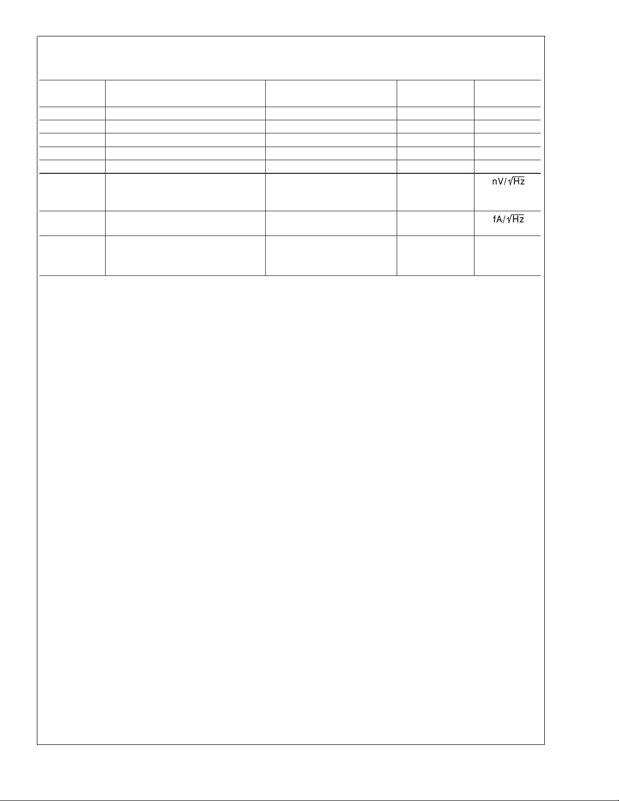
DC Electrical Characteristics
Unless otherwise specified, all limits guaranteed for T
Boldface limits apply at the temperature extremes.
Symbol Parameter Conditions
V
OS
TCV
OS
Input Offset Voltage 0.5 5 mV
Input Offset Voltage 2.3 µV/˚C
Average Drift
I
IN
I
OS
R
IN
Input Current (Note 11) 0.02 pA
Input Offset Current (Note 11) 0.01 pA
Input Resistance
CMRR Common Mode 0.7V ≤ V
+
Rejection Ratio V
=
+PSRR Positive Power Supply 5V ≤ V
Rejection Ratio V
O
−PSRR Negative Power Supply 0V ≤ V
Rejection Ratio V
V
CM
Input Common-Mode V
O
+
=
Voltage Range For CMRR ≥ 40 dB 0.5 max
+
=
V
For CMRR ≥ 40 dB 0.3 max
+
=
V
For CMRR ≥ 50 dB 0.0 max
+
=
V
For CMRR ≥ 50 dB 0.0 max
=
25˚C, V
J
≤ 12.7V 96 63 dB
CM
15V 60 min
+
≤ 15V, 93 63 dB
=
2.5V 60 min
−
≤ −10V 97 74 dB
2.5V, V
+
=
5V 70 min
=
2.7V −0.1 0.3 V
3V −0.3 0.1 V
5V −0.5 −0.2 V
15V −0.5 −0.2 V
Storage Temperature Range −65˚C to +150˚C
Junction Temperature (Note 4) 150˚C
Operating Ratings (Note 1)
Supply Voltage 2.0V to 15.5V
Temperature Range
L
≤ +85˚C
J
>
1MΩ.
UnitsLMC6036I
LMC6035I and LMC6036I −40˚C ≤ T
Thermal Resistance (θ
)
JA
MSOP, 8-pin Mini Surface Mount 230˚C/W
M Package, 8-pin Surface Mount 175˚C/W
M Package, 14-pin Surface Mount 127˚C/W
MTC Package, 14-pin TSSOP 137˚C/W
BP, 8-Bump micro SMD Package 220˚C/W
+
=
2.7V, V
−
=
0V, V
CM
=
1.0V, V
=
1.35V and R
O
LMC6035I
Typ
(Note 5)
Limit (Note 6)
6 max
90 max
45 max
>
10 Tera Ω
2.3 2.0 V
1.7 min
2.6 2.3 V
2.0 min
4.5 4.2 V
3.9 min
14.4 14.0 V
13.7 min
www.national.com3
DC Electrical Characteristics (Continued)
Unless otherwise specified, all limits guaranteed for T
Boldface limits apply at the temperature extremes.
Symbol Parameter Conditions
LMC6035/LMC6036
A
V
Large Signal Voltage Gain R
L
(Note 7) 75 min
=
R
L
V
O
I
O
I
S
Output Swing V
Output Current V
Supply Current LMC6035 for Both Amplifiers 0.65 1.6 mA
+
R
L
+
V
R
L
+
V
R
L
+
V
R
L
O
V
O
V
O
LMC6036 for All Four Amplifiers 1.3 2.7 mA
V
O
=
J
=
600Ω Sourcing 1000 100 V/mV
2kΩ Sourcing 2000 V/mV
=
2.7V 2.5 2.0 V
=
600Ω to 1.35V 1.8 min
=
2.7V 2.62 2.4 V
=
2kΩto 1.35V 2.2 min
=
15V 14.5 13.5 V
=
600Ω to 7.5V 13.0 min
=
15V 14.8 14.2 V
=
2kΩto 7.5V 13.5 min
=
0V Sourcing 8 4 mA
=
2.7V Sinking 5 3 mA
=
1.35V 1.9 max
=
1.35V 3.0 max
25˚C, V
+
=
2.7V, V
−
=
0V, V
CM
=
1.0V, V
=
1.35V and R
O
L
>
1MΩ.
LMC6035I
Typ
(Note 5)
UnitsLMC6036I
Limit (Note 6)
Sinking 250 25 V/mV
20 min
Sinking 500 V/mV
0.2 0.5 V
0.7 max
0.07 0.2 V
0.4 max
0.36 1.25 V
1.50 max
0.12 0.4 V
0.5 max
3 min
2 min
www.national.com 4
LMC6035/LMC6036
AC Electrical Characteristics
25˚C, V
+
=
Unless otherwise specified, all limits guaranteed for T
1MΩ.Boldface limits apply at the temperature extremes.
=
J
Symbol Parameter Conditions Typ Units
SR Slew Rate (Note 9) 1.5 V/µs
+
GBW Gain Bandwidth Product V
θ
m
G
m
Phase Margin 48 ˚
Gain Margin 17 dB
=
15V 1.4 MHz
Amp-to-Amp Isolation (Note 10) 130 dB
e
n
i
n
Input-Referred Voltage Noise f=1 kHz 27
=
V
CM
1V
Input Referred Current Noise f=1 kHz 0.2
THD Total Harmonic Distortion f=10 kHz, A
=
R
2kΩ,V
L
+
=
V
10V
Note 1: Absolute Maximum Ratings indicate limits beyond which damage to the device may occur. Operating Ratings indicate conditions for which the device is intended to be functional, but specific performance is not guaranteed. For guaranteed specifications and the test conditions, see the Electrical Characteristics.
Note 2: Human body model, 1.5 kΩ in series with 100 pF.
Note 3: Applies to both single-supply and split-supply operation. Continuous short circuit operation at elevated ambient temperature can result in exceeding the
maximum allowed junction temperature of 150˚C. Output currents in excess of 30 mA over long term may adversely affect reliabilty.
Note 4: Themaximum power dissipation is a function of T
−TA)/θJA. All numbers apply for packages soldered directly onto a PC board with no air flow.
Note 5: Typical Values represent the most likely parametric norm or one sigma value.
Note 6: All limits are guaranteed by testing or statistical analysis.
Note 7: V
Note 8: Do not short circuit output to V
Note 9: V
Note 10: Input referred, V
Note 11: Guaranteed by design.
+
=
15V, V
+
=
15V. Connected as voltage follower with 10V step input. Number specified is the slower of the positive and negative slew rates.
CM
=
7.5V and R
+
=
15V and R
connected to 7.5V. For Sourcing tests, 7.5V ≤ VO≤ 11.5V. For Sinking tests, 3.5V ≤ VO≤ 7.5V.
L
+
when V+is greater than 13V or reliability will be adversely affected.
=
100 kΩ connected to 7.5V. Each amp excited in turn with 1 kHz to produce V
L
, θJA, and TA. The maximum allowable power dissipation at any ambient temperature is P
J(max)
2.7V, V
V
O
−
=
0V, V
CM
=
1.0V, V
=
1.35V and R
O
>
L
(Note 5)
=
−10
=
8V
PP
0.01
=
.
12 V
O
PP
%
=
(T
D
J(max)
www.national.com5
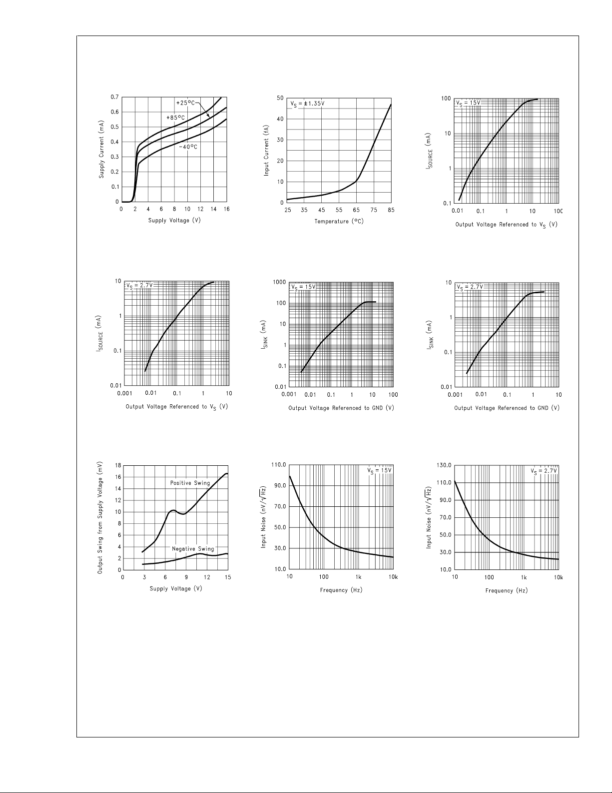
Typical Performance Characteristics Unless otherwise specified, V
=
2.7V, single supply, T
S
=
25˚C
A
Supply Current vs
Supply Voltage (Per Amplifier)
LMC6035/LMC6036
Sourcing Current vs
Output Voltage
DS012830-52
Input Current vs
Temperature
Sinking Current vs
Output Voltage
DS012830-53
Sourcing Current vs
Output Voltage
DS012830-54
Sinking Current vs
Output Voltage
Output Voltage Swing vs
Supply Voltage
DS012830-55
DS012830-58
Input Noise vs
Frequency
DS012830-56
DS012830-59
DS012830-57
Input Noise vs
Frequency
DS012830-60
www.national.com 6
 Loading...